 E-mail Alert
 RSS
RSS-
Abstract
A tunable plasmofluidic lens consisting of nanoslit arrays on a metal film is proposed for subwavelength imaging in far field at different wavelengths. The nanoslit arrays with constant depths but varying widths could generate desired optical phase retardations based on the propagation property of the surface plasmon polaritons (SPPs) through the metal-dielectric-metal (MDM) nanoslit waveguide. We demonstrate the tunability of the plasmofluidic lens for subwavelength imaging by changing the surrounding dielectric fluid. This work provides a novel approach for developing integrative tunable plasmofluidic lens for a variety of lab-on-chip applications.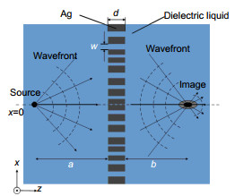
-
1. Introduction
Fluids have unique properties that cannot be found in solids and these properties can be used to design novel devices, such as oil-immersion microscopes [11], liquid mirrors for telescopes [12], liquid-crystal displays [13] and tunable liquid gradient refractive index lenses [14]. Integration and reconfiguration are the two main advantages of optofluidics. The second advantage of optofluidics means that one can easily change the optical properties of the devices by controlling the fluids [15]. Therefore, in this paper, we propose a tunable plasmofluidic lens for subwavelength imaging at different incident wavelengths by varying the surrounding dielectric fluid.
On the other hand, as indicated in Ref. [7], a planar metallic slab with arrayed nanoslits of varying widths could be demonstrated theoretically [8] and experimentally [9] to focus light in far field. A planar plasmonic lens has been proposed to realize subwavelength imaging for arbitrary object and image distances [10]. Based on the optimum design of nanoslit waveguides in the metallic slab, the imaging process is achieved by manipulating the phase distribution of the optical field. Each nanoslit in the metallic slab is designed to transmit light with specific phase retardation, therefore arbitrary phase modulation on the wavefront could be realized. However, due to the dependence of permittivity of metallic materials on frequencies, applications would be limited because the plasmonic lens can only operate at a specific frequency when the geometries of the nanoslits are fixed.
Recently, the optical diffraction limit has been overcome by the perfect lens proposed by Pendry using a slab of negative refractive index (NRI) media [1]. However, the difficulty of finding a homogenous NRI media restrains the practical applications of the perfect lens. Considering the electrostatic approximation of the perfect lens, the super-lens could also be used to realize sub-diffraction- limited imaging, only requiring negative permittivity that is available in natural metals in particular frequency regimes. Therefore, impressive works concerning superlenses have been achieved theoretically and experimentally [2-4]. However, the shortcoming of the superlens is that the object and image should be confined in near field, usually tens of nanometers away from the superlens [1, 5]. Therefore, an optical far-field superlens (FSL) has been designed for imaging beyond the diffraction limit in far field [6].
2. Working principle
where d is the thickness of the plasmonic slab, and θ originates from the multiple reflections between the entrance and exit surfaces of the slab. Both physical analysis and numerical simulations show that the phase retardation is dominantly determined by the real part of β [8]. Therefore, △φ can be approximated as Re(βd), and it could be obtained from Eqs. (2) and (3) that the phase retardation can be tuned by changing the slit width when other parameters are fixed [8-10]. According to Eqs. (2) and (3), if λ=730 nm, εd=1.769(
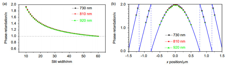
${\varepsilon _{\rm{d}}} = n_{\rm{d}}^2$ , H2O) and d=200 nm, the width of each nanoslit at position x could be designed to meet the requirement of phase distribution depicted in Fig. 2(a), as shown in Fig. 2(b).For example, we choose other two different incident wavelengths at 810 nm and 920 nm, with corresponding permittivities of the dielectric fluids at 2.200 (carbon tetrachloride, CCl4) and 2.846 (phosphorus tribromide, PBr3) [22], respectively. Other parameters are the same as mentioned above. According to Eq. (2), it could be observed in Fig. 3(a) that the phase retardation of light transmitted through each nanoslit deviates slightly from one another at three different incident wavelengths. The thickness of the metallic wall between two adjacent nanoslits should be larger than the skin depth in metal to prevent the coupling of SPPs during the propagation process. Therefore, the width of the nanoslit should not be large and the maximum value of the width is set as 60 nm. When the positions and widths of nanoslits are fixed as such in Fig. 2(b), the calculated phase retardations of the same arrayed nanoslits in the plasmonic lens at three different wavelengths agree well with each other, as shown in Fig. 3(b).
When transverse magnetic (TM) polarized waves impinge on the entrance surface of the silver slab, surface plasmon polaritons (SPPs) are excited [17]. SPPs propagate through the nanoslit region with specific waveguide modes until they reach the exit surface where they return into the light mode [17-18]. It is the diffraction and interference of the surface plasmon waves that contribute to the transition from the evanescent waves to the propagating waves in far field [19], which is the coupling mechanism for far field super-resolution imaging [6]. Therefore, it is theoretically possible for the plasmonic lens to achieve subwavelength imaging in far field [10]. For an electromagnetic wave incident on such a plasmonic lens, the phase change of the wave is sensitive to the length [7], width [8, 20], and material inside the slit as it passes through each nanoslit [21]. In the previous works, the influence of the length and width of the nanoslits on the phase change have been theoretically investigated and widely used for different purposes. In contrast, in this paper, a tunable plasmonic lens is proposed for subwavelength imaging at different wavelengths by varying the surrounding dielectric material while holding nanoslits' lengths, widths and positions constant.
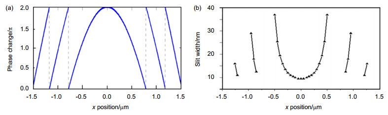
![Figure 2. (a) Required phase change for the point-to-point imaging of an object localized on the axis x=0 as a function of x, which is the position of each nanoslit. (b) Distribution of widths and positions of nanoslits in the plasmofluidic lens.]() Figure 2.
Figure 2.(a) Required phase change for the point-to-point imaging of an object localized on the axis x=0 as a function of x, which is the position of each nanoslit. (b) Distribution of widths and positions of nanoslits in the plasmofluidic lens.
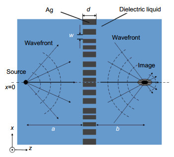
Fig. 1 is the schematic drawing of the optical imaging process for the tunable plasmonic lens. The plasmonic lens is a silver slab of thickness d with nanoslits located symmetrically with respect to x=0 plane, represented by the dashed line in Fig. 1. The width of each nanoslit is w. The object (a point light source) is located on the left side of the lens at a distance of a, and the image on the right side at a distance of b. The plasmonic lens is immersed inside the dielectric liquid with permittivity εd, and each nanoslit could be also filled with the dielectric liquid. All the components are treated as semi-infinite in y direction. The Drude model
${\varepsilon _{\rm{m}}} = {\varepsilon _\infty } - \omega _{\rm{p}}^2/[\omega (\omega + {\rm{i}}{V_{\rm{c}}})]$ is used to describe the permittivity of silver at different frequencies, where ε∞ =3.2938, plasma frequency ωp=1.3552x10¹⁶ rad/s and collision frequency Vc=1.9944x10¹⁴ rad/s [16]. All the materials are assumed to be nonmagnetic so that the magnetic permeability μ is equal to 1 and only the permittivity ε has been taken into account.On the other hand, assuming that the width of each nanoslit w is much smaller than the incident wavelength, it is reasonable for just considering the fundamental mode in the nanoslit [5]. The complex propagation constant β in the slit can be determined by the equation [8, 23]:
However, as the incident wavelength changes while other parameters are fixed, the required phase change calculated by Eq. (1) and the permittivity of metal εm would vary, resulting in the change of propagation constant β in each slit according to Eq. (2). Therefore, the point-to-point subwavelength imaging could not be achieved again. There are two ways to solve this problem. Firstly, we could change the positions and widths of the nanoslits to fulfill the requirement of phase change as the incident wavelength varies. Obviously, this is unpractical because we should use different plasmonic lenses to achieve subwavelength imaging at different wavelengths. Secondly, it is possible for subwavelength imaging at different wavelengths by simply varying the surrounding dielectric material. The only requirement for the second method is that we should choose different dielectric fluids (nd) to keep the effective wavelength
${\lambda _{{\rm{eff}}}} = \lambda /{n_{\rm{d}}}$ invariable as the incident wave length λ changes.![Figure 3. (a) Dependence of the phase retardation on the slit width at three different wavelengths. The incident wavelengths are 730 nm, 810 nm and 920 nm. (b) Calculated phase retardations of the arrayed nanoslits in the plasmonic lens at three different wavelengths when the widths and positions of nanoslits are fixed. The blue curve represents the required phase change for the subwavelength imaging.]() Figure 3.
Figure 3.(a) Dependence of the phase retardation on the slit width at three different wavelengths. The incident wavelengths are 730 nm, 810 nm and 920 nm. (b) Calculated phase retardations of the arrayed nanoslits in the plasmonic lens at three different wavelengths when the widths and positions of nanoslits are fixed. The blue curve represents the required phase change for the subwavelength imaging.
where k0 is the wave vector of free space light, εd and εm represent the permittivities of the dielectric inside the nanoslit and metal, respectively. It is clearly seen from this equation that the propagation constant β changes as the slit width w varies, when k0, εd and εm are fixed. The real and imaginary parts of β respectively determine the phase velocity and propagation loss of SPPs in the nanoslit. The phase retardation of light transmitting through the nanoslit can be expressed as:
On the one hand, it is clearly seen in Eq. (1) that if the effective wavelength λ/nd is constant while the incident wavelength λ changes, the required phase change at position x for the point-to-point imaging will be invariable, as shown in Fig. 2(a). In other words, we could realize subwavelength imaging of the same object at the same position as long as λ/nd is invariable. On the other hand, when the position and width of nanoslit are fixed, the phase retardation of light transmitted through the nanoslit
$\Delta \varphi = {\mathop{\rm Re}\nolimits} (\beta d)$ should be also invariable at different incident wavelengths to coincide with the unchanged phase distribution shown in Fig. 2(a). Fortunately, in Eq. (2), as the dielectric material (${\varepsilon _{\rm{d}}} = n_{\rm{d}}^2$ ) varies to fulfill the requirement of the invariable effective wavelength λ/nd at different incident wavelengths, the propagation constant β in each nanoslit changes so little that it could be ignored. The phase retardation of light transmitted through the nanoslit$\Delta \varphi = {\mathop{\rm Re}\nolimits} (\beta d)$ could also be maintained at different wavelengths. Therefore, both the required phase change and phase retardation are invariable at different incident wavelengths, resulting in that the imaging process will be slightly influenced by the wavelength variability.where n is an arbitrary integer number, nd is the refractive index of the surrounding dielectric material, λ represents the incident wavelength, and x is the position of each nanoslit. For example, when we choose λ=730 nm, a=1 μm, b=1 μm and nd=1.33 (water, H2O) [22], the required phase change at different x positions calculated by Eq. (1) is shown in Fig. 2(a).
According to the equal optical length principle, the required phase distribution of light for the point-to-point imaging of an object localized on the axis x=0 can be obtained by:
3. Numerical simulation and discussion
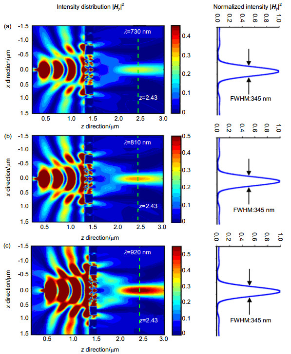
Numerical calculations were carried out by using finite-difference time-domain (FDTD) method to illustrate the validity of the tunable plasmonic lens. The simulation dimension is 3 μm×3 μm with a grid size of 2 nm. The point light sources, which are positioned at the point x=0, z=0.3 μm, should be small enough and they are designated to be λ/10 at different incident wavelengths. The plasmonic lens is located between the plane at z=1.3 μm and z=1.5 μm. Around the simulation region is the perfectly matched layer (PML) boundary condition. As mentioned above, the incident wavelengths are 730 nm, 810 nm and 920 nm, and the corresponding permittivities of the dielectric materials are 1.769, 2.200 and 2.846, respectively. The other parameters are the same as before. The calculated optical field distributions of the simulation results are shown at the left side of Figs. 4(a), 4(b) and 4(c). The cross sections of image plane at z=2.43 μm are given at the right side of Figs. 4(a), 4(b) and 4(c).
From the left side of Figs. 4(a)~4(c), it can be seen that the optical intensity distributions exhibit similarity to one another at three different wavelengths. The full width at half maximum (FWHM) of the image spots at these three different wavelengths are all equal to 345 nm (0.37λ~0.47λ), as shown at the right side of Figs. 4(a)~4(c). This is reasonable because the required phase change and phase retardations of the same arrayed nanoslits are invariable at these three wavelengths. Therefore, the imaging process is slightly influenced by the wavelength variability and FWHM of image spots are the same as each other. The only difference is that the intensity value becomes larger as the incident wavelength increases. The reason is that as the incident wavelength λ increases the point light source (λ/10) becomes larger, resulting in the enhancement of the optical field intensity. Furthermore, the image spot is supposed to be located at the point of x=0, z=2.5 μm because the designed image distance is b=1 μm. The slight focal shift of about 70 nm mainly originates from the discreteness of nanoslits and coupling effect of SPPs from the adjacent nanoslits. The overall focusing efficiency of the lens is around 45%~55% (Pfocus/Pin), which is relatively high for practical applications.
![Figure 4. Calculated optical field distribution of the simulation result (left) and cross section of image plane at z=2.43 μm (right) is shown at wavelengths (a) 730 nm, (b) 810 nm and (c) 920 nm. The light source is localized at point x=0, z=0.3 μm, and the plasmonic lens ranges from z=1.3 μm to z=1.5 μm.]() Figure 4.
Figure 4.Calculated optical field distribution of the simulation result (left) and cross section of image plane at z=2.43 μm (right) is shown at wavelengths (a) 730 nm, (b) 810 nm and (c) 920 nm. The light source is localized at point x=0, z=0.3 μm, and the plasmonic lens ranges from z=1.3 μm to z=1.5 μm.
From the left side of Figs. 4(a)~4(c), it can be seen that the optical intensity distributions exhibit similarity to one another at three different wavelengths. The full width at half maximum (FWHM) of the image spots at these three different wavelengths are all equal to 345 nm (0.37λ~0.47λ), as shown at the right side of Figs. 4(a)~4(c). This is reasonable because the required phase change and phase retardations of the same arrayed nanoslits are invariable at these three wavelengths. Therefore, the imaging process is slightly influenced by the wavelength variability and FWHM of image spots are the same as each other. The only difference is that the intensity value becomes larger as the incident wavelength increases. The reason is that as the incident wavelength λ increases the point light source (λ/10) becomes larger, resulting in the enhancement of the optical field intensity. Furthermore, the image spot is supposed to be located at the point of x=0, z=2.5 μm because the designed image distance is b=1 μm. The slight focal shift of about 70 nm mainly originates from the discreteness of nanoslits and coupling effect of SPPs from the adjacent nanoslits. The overall focusing efficiency of the lens is around 45%~55% (Pfocus/Pin), which is relatively high for practical applications.
4. Conclusions
In summary, based on the combination of the particular propagation property of SPPs in nanoslit waveguides and microfluidics, we proposed a tunable plasmofluidic lens for realizing subwavelength imaging in far field with different incident wavelengths simply by changing the surrounding dielectric fluid. The numerical simulation performed by FDTD method agrees well with the theoretical analysis, and it is shown that the imaging process is slightly influenced by incident wavelength. The tunable plasmonic lens could be easily extended to three dimensional and have novel applications in nanophotonics [24], nanolithography [25-26], and optical-based on-chip analysis [15] etc.
-
参考文献
Pendry J B. Negative refraction makes a perfect lens[J]. Physical Review Letters, 2000, 85: 3966-3969.
DOI: 10.1103/PhysRevLett.85.3966Ramakrishna S A, Pendry J B, Schurig D, et al. The asymmetric lossy near-perfect lens[J]. Journal of Modern Optics, 2002, 49(10): 1747-1762.
DOI: 10.1080/09500340110120950Fang N, Lee H, Sun Cheng, et al. Sub-diffraction-limited optical imaging with a silver superlens[J]. Science, 2005, 308(5721): 534-537.
DOI: 10.1126/science.1108759Lee H, Xiong Yi, Fang N, et al. Realization of optical superlens imaging below the diffraction limit[J]. New Journal of Physics, 2005, 7: 255.
DOI: 10.1088/1367-2630/7/1/255展开 -
版权信息
版权属于中国科学院光电技术研究所,但文章内容可以在本网站免费下载,以及免费用于学习和科研工作 -
关于本文
出版历程
- 收稿日期 2016-11-11
- 修回日期 2016-12-25
- 刊出日期 2017-03-14
文章计量
访问数(6801) PDF下载数(2418)
- 6801 访问数
- 2418 下载数
 下载:
下载: