E-mail Alert
 RSS
RSS-
Abstract
Over the past two decades, femtosecond laser-induced periodic structures (femtosecond-LIPSs) have become ubiquitous in a variety of materials, including metals, semiconductors, dielectrics, and polymers. Femtosecond-LIPSs have become a useful laser processing method, with broad prospects in adjusting material properties such as structural color, data storage, light absorption, and luminescence. This review discusses the formation mechanism of LIPSs, specifically the LIPS formation processes based on the pump-probe imaging method. The pulse shaping of a femtosecond laser in terms of the time/frequency, polarization, and spatial distribution is an efficient method for fabricating high-quality LIPSs. Various LIPS applications are also briefly introduced. The last part of this paper discusses the LIPS formation mechanism, as well as the high-efficiency and high-quality processing of LIPSs using shaped ultrafast lasers and their applications.
Keywords
-
Introduction
Femtosecond-LIPSs have become a useful laser processing method, with broad prospects for adjusting material properties9, 32-38 . HSFLs on the surfaces and interiors of dielectrics demonstrate birefringence effects, which have been used in data storage and waveplates34, 36, 38. LIPSs produce a significant dispersion of incident light and have been used to prepare pure and bright structural color surface32, 35. Composite structures with LIPSs can enhance light absorption and luminescence and adjust the wetting properties of a material surface33, 37, 39. The anisotropic electrical properties of LIPSs are an emerging research topic40, 41.
The main contents of this review are as follows. Section Several models of LIPS formation discusses the formation mechanism of LIPSs. Section Ultrafast dynamics of LIPS formation based on pump-probe imaging presents the ultrafast dynamics studied by the pump-probe imaging method. The pulse shaping of a femtosecond laser in the temporal–frequency domain, polarization, and spatial distribution is an efficient method for fabricating regular LIPSs with high efficiency, as described in Section Efficient fabrication of high-quality LIPSs with shaped ultrafast laser pulses. Section Femtosecond laser direct writing of <100 nm nanostructures introduces promising methods for laser processing nanostructures with feature sizes smaller than 100 nm. In the Section Applications of LIPSs, we briefly introduce LIPS applications in the fields of data storage, structural color surfaces, light absorption and luminescence enhancement, and the adjustment of conductive properties. The last section presents the outlook on the LIPSs. storage, structural color surfaces, light absorption and luminescence enhancement, and the adjustment of conductive properties. The last section presents the outlook on the LIPSs.
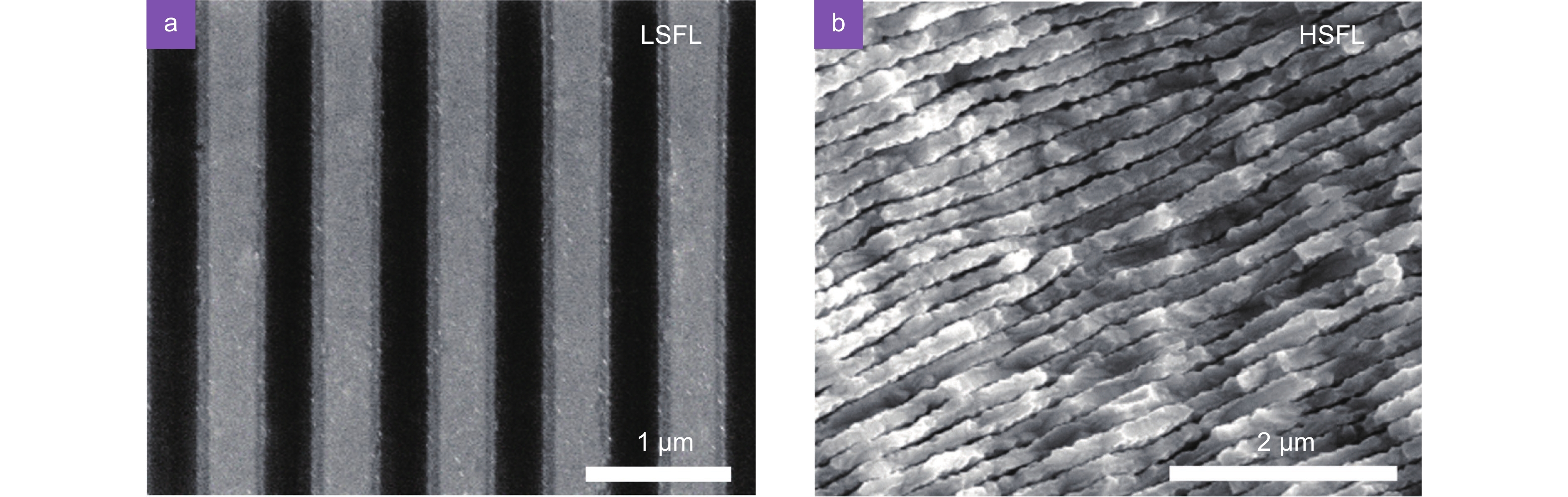
Laser-induced periodic structures (LIPSs) have been intensively studied since 1965 when Birnbaum et al. found LIPSs on the surface of germanium and gallium arsenide15, 16. Over the past two decades, ultrafast laser technology has developed rapidly. Femtosecond LIPSs (femtosecond-LIPSs) have become ubiquitous in a variety of materials, including metals, semiconductors, dielectrics, and polymers4-9, 17-31. The periods of LIPSs change significantly with the laser fluence and the number of overlapping pulses. Based on the ratio of the period (Λ) to the laser wavelength (λ), LIPSs are divided into low-spatial-frequency LIPSs (LSFLs, Λ>0.5λ) and high-spatial-frequency LIPSs (HSFLs, Λ<0.5λ)4, as shown in Fig. 1. However, the formation mechanism of femtosecond-LIPSs does not yet have a clear explanation.
Femtosecond lasers have ultrashort pulse durations and high peak powers1. The interaction between femtosecond laser and matter has the advantages of minimal thermal effect and no material selectivity2, 3. Compared with nanosecond and other long-pulse lasers, femtosecond lasers could induce more regular and deeper periodic structures on different types of materials, such as metals, semiconductors, dielectrics, and polymers, without being overwhelmed by huge thermal effects4-14.
Several models of LIPS formation
The formation of periodic nanostructures after irradiation with a single laser beam is an interesting phenomenon. In particular, the periods of femtosecond-LIPSs change significantly with the laser fluence and the number of overlapping pulses, which renders the formation mechanism of LIPSs more complicated to determine. Numerous experimental, theoretical, and numerical studies have been performed, and several models have been proposed to explain the formation of LIPSs9, 16-18, 20, 21, 25, 42, which are described below.
Scattering light model
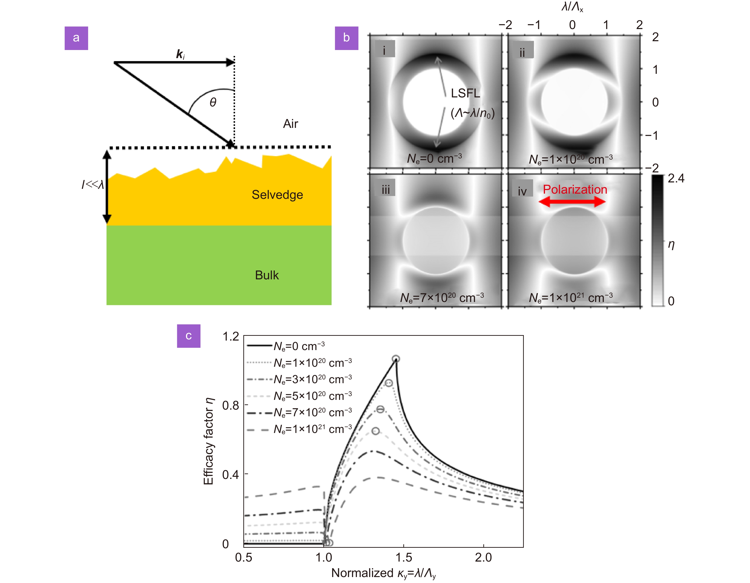
After irradiation with continuous and long-pulse lasers, LSFLs perpendicular or parallel to the polarization direction formed on the surfaces of semiconductor materials, where the periods were nearly equal to the laser wavelength, λ. It was proposed that these LSFLs were caused by the interference between the incident light and scattered light from the ablated surface16, 18, 43, as shown in Fig. 2. When the laser was perpendicular to the sample, period Λ was equal to laser wavelength λ. When the laser was obliquely incident at an angle θ, period Λ = λ/ (1 ± sin θ), where + and – represent the forward and backward scattered light, respectively44. This model was refined and developed by Sipe et al. They performed detailed theoretical studies and found that the generation of periodic structures depended significantly on the roughness of the material surface16. Rough structures with a height significantly smaller than the laser wavelength resulted in a periodic distribution of the laser field itself. The incident angle and polarization direction highly influenced the period and orientation of the LSFLs. This model has often been used to explain classical LSFLs induced by nanosecond or continuous wave (CW) lasers.
Over the last two decades, scattering models have been developed and improved to explain the formation of femtosecond-LIPSs45, 46. According to the Drude model, the dielectric constants of semiconductors and dielectrics depend on the numerical density of free electrons excited by femtosecond laser. According to the Sipe model, the periodic deposition of laser energy depends on the surface roughness and dielectric constants. The formation of femtosecond-LIPSs on semiconductors and dielectrics was studied by comprehensively considering the Sipe and Drude models22, 23, 47, 48, and developed into the Sipe-Drude model22. The numerical density of free electrons and dielectric constants varied with the laser fluence, wavelength, and pulse number, which further tuned the periods of LIPSs, as shown in Fig. 2.
![Figure 2. (a) The schematic of light irradiated on a rough surface at an incident angle θ, where ki is the wave-vector component parallel to the surface, and l is the thickness of selvedge region. (b) The efficacy factor η as a function of the normalized LIPS wave vector for silica at different excited state. (c) The efficacy factor η along the positive ky-axis for silica at different excitation levels, with circles marking ky-positions where LIPS formation could be expected. Figure reproduced with permission from: (a) ref.16, American Physical Society; (b, c) ref.22, AIP Publishing.]()
(a) The schematic of light irradiated on a rough surface at an incident angle θ, where ki is the wave-vector component parallel to the surface, and l is the thickness of selvedge region. (b) The efficacy factor η as a function of the normalized LIPS wave vector for silica at different excited state. (c) The efficacy factor η along the positive ky-axis for silica at different excitation levels, with circles marking ky-positions where LIPS formation could be expected. Figure reproduced with permission from: (a) ref.16, American Physical Society; (b, c) ref.22, AIP Publishing.
Surface plasmon polariton model
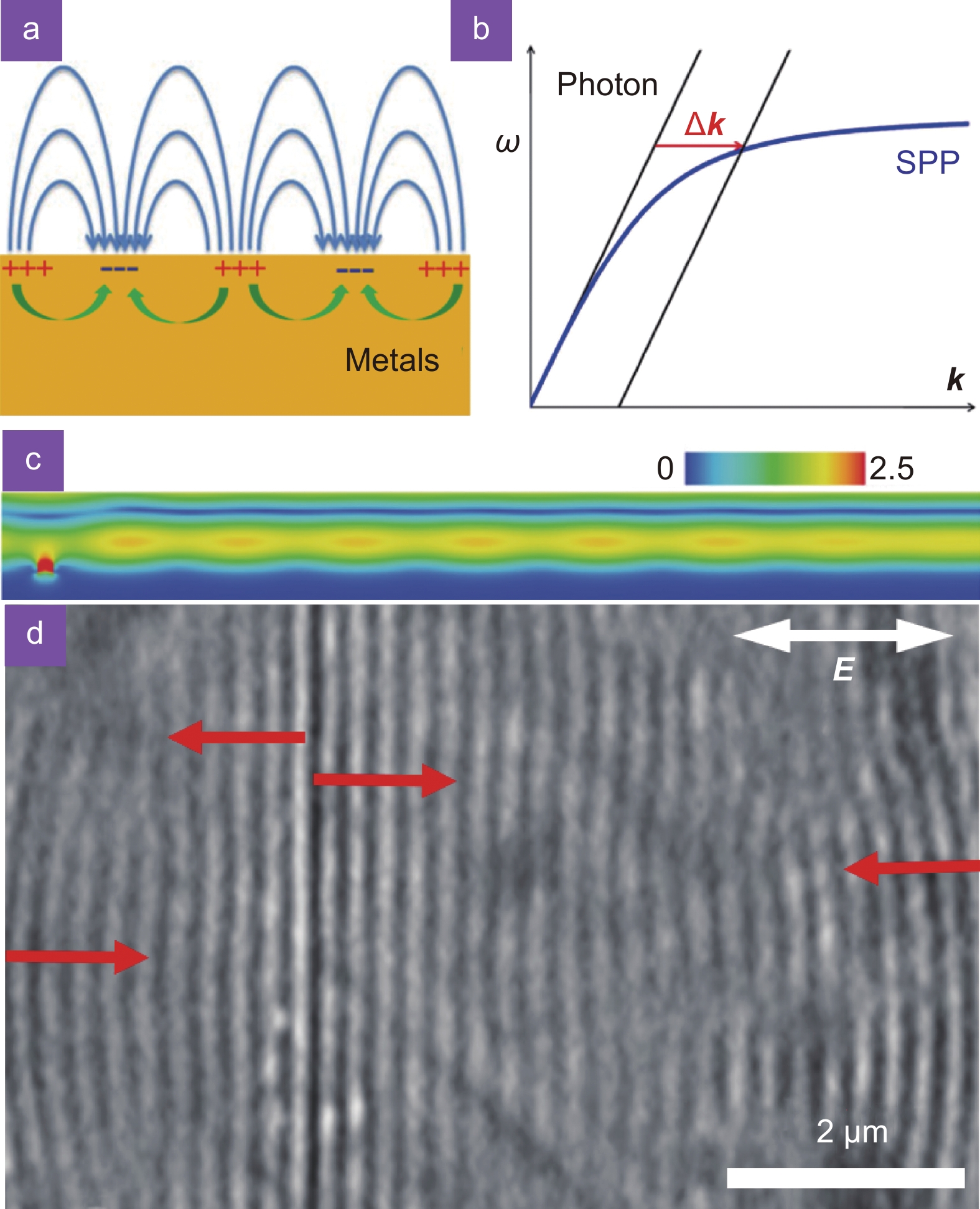
The SPP model was used to explain the formation of LSFLs on semiconductors. The periods are expressed as follows21
![Figure 3. (a) Schematic illustration of SPPs. (b) Dispersion curves of SPPs and light in air. (c) SPP excitation on ZnO surface in the excited state launched by a groove. (d) The SEM image of the nanostructures on the ZnO surface irradiated by 800 nm femtosecond laser, where the LSFLs originated from the nanogroove or the ablation edge, as shown as the red arrows. Figure reproduced with permission from: (b) ref.49, AIP Publishing; (c, d) ref.21, American Chemical Society.]()
(a) Schematic illustration of SPPs. (b) Dispersion curves of SPPs and light in air. (c) SPP excitation on ZnO surface in the excited state launched by a groove. (d) The SEM image of the nanostructures on the ZnO surface irradiated by 800 nm femtosecond laser, where the LSFLs originated from the nanogroove or the ablation edge, as shown as the red arrows. Figure reproduced with permission from: (b) ref.49, AIP Publishing; (c, d) ref.21, American Chemical Society.
Under femtosecond laser irradiation, a large number of free electrons are excited, forming a plasma layer on the surface of a material. The femtosecond laser further causes the collective oscillation of the surface plasma and forms surface plasmon polaritons (SPPs), as shown in Fig. 3(a). The excitation of SPPs causes a periodic distribution of the laser field and energy deposition in the free electrons. The lattice is heated, melted, or even ablated via electron–phonon coupling, which further induces the formation of LIPSs8, 21, 25, 48, 50-62. However, in the case of vertical incidence (Fig. 3(b)), the wave vector of the SPPs is always larger than that of the incidence light. Therefore, grating structures42 or a single nanogroove25, 52 are fabricated on the sample surface in advance, and the scattered light can provide an additional wave vector, Δk, which satisfies the vector matching condition and induces SPP excitation, as shown in Fig. 3(c)21.
Λ=λλλSPP±sin(θ),λSPP=λ×Re(√ϵ+ϵdϵϵd), where λSPP is the SPP wavelength, θ is the angle of incidence, ε is the dielectric constant of the metal, and εd is the dielectric constant of the dielectric. Under femtosecond laser irradiation, a large number of free electrons are excited, resulting in a significant change in the dielectric constant, according to the Drude model. The SPP wavelength and LSFL period can be calculated based on the dielectric constant in the excited state, which agrees well with the experimental results for semiconductors42, 51, 52. The LSFL periods induced by femtosecond laser pulses on semiconductors and metals are always smaller than the SPP wavelengths. With more laser pulse irradiation, the LSFL-assisted SPP is coupled with the laser field, forming a positive feedback effect, and leading to the formation of shorter-period LSFLs21.
Model of nanoplasmonic enhancement of laser field
Another mechanism that has been proposed for the formation of HSFLs in fused silica is photon–plasmon scattering17. By adjusting the pulse energy and cumulative pulse number of the 800 nm femtosecond laser, the HSFLs period varied from 140 to 320 nm. This phenomenon was interpreted in terms of the interference between the incident light field and the electric field of the bulk plasma wave, resulting in the periodic modulation of the electron concentration and structural changes in the fused silica17.
The periodic distribution of the nanoplanes evolved from a random distribution of nanoplasma over many shots owing to the memory mechanism and mode selection. The period, λ0/2n, is the minimum spacing required in planar metal waveguides to support this mode with the field maxima at the metal–dielectric interface20.
![Figure 4. (a) SEM image of HSFLs inside fused silica induced by 800 nm femtosecond laser pulses. (b) Nanoplasma growth into plane governed by local field distribution, where Epol and Eeq are the local fields on the polar axis and in the equatorial plane, respectively4, 20. Figure reproduced with permission from: (a) ref.20, American Physical Society.]()
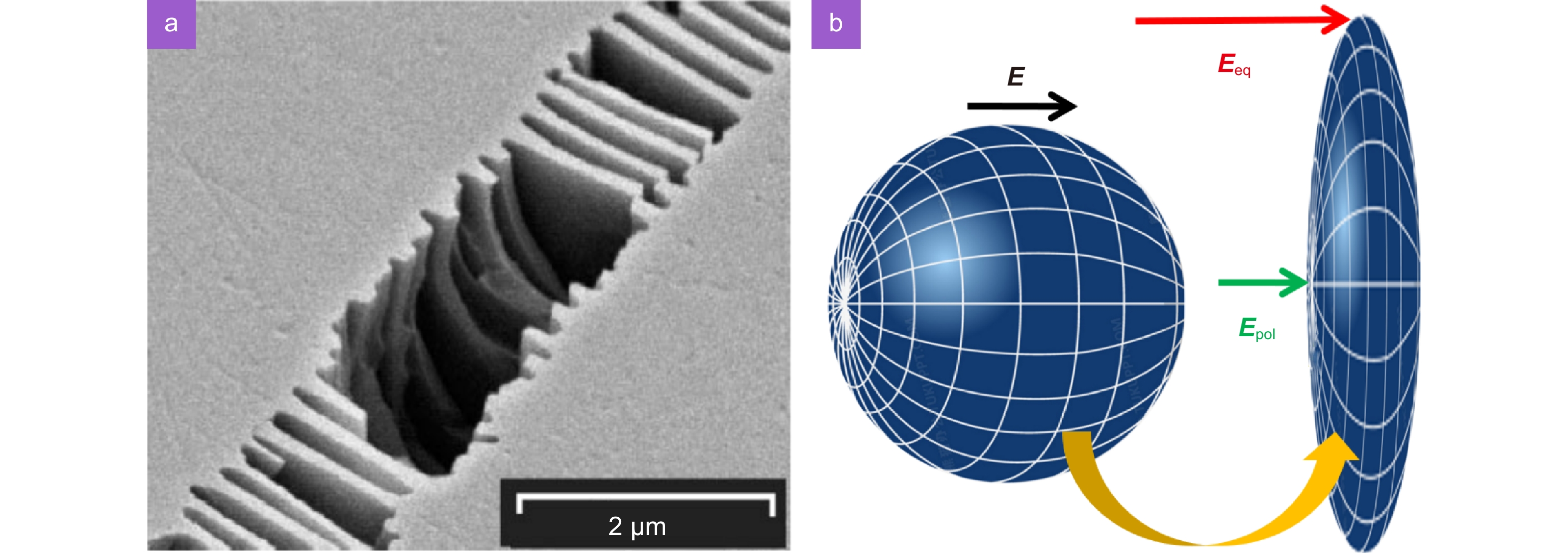
(a) SEM image of HSFLs inside fused silica induced by 800 nm femtosecond laser pulses. (b) Nanoplasma growth into plane governed by local field distribution, where Epol and Eeq are the local fields on the polar axis and in the equatorial plane, respectively4, 20. Figure reproduced with permission from: (a) ref.20, American Physical Society.
The groove widths of HSFLs induced by femtosecond laser pulses are usually smaller than 100 nm, whereas the depth can reach hundreds of nanometers to micrometers. The widths of these periodically arranged nanogrooves are significantly smaller than the diffraction limit of the laser17, 20, 63-72. Figure 4(a) shows 20 nm-thick nanosheet-like nanostructures with a period of ~λ/2n in fused silica (refractive index n) induced by linearly polarized 800 nm femtosecond laser pulses. It was proposed that these nanosheets were produced by the asymmetrically localized laser-field enhancement of the nanoplasma20, as shown in Fig. 4(b).
Other models
In recent years, several other models have been proposed to explain the formation of LIPSs, such as self-organization24, 26, 73, evanescent waves74, and Coulomb explosions75, 76. During the femtosecond laser irradiation of SiC, ZnSe, and ZnO crystals, the generation of second harmonics induces the formation of HSFLs9, 77, 78. The ripples of LSFLs on metal surfaces gradually split and evolve into HSFLs with an increase in femtosecond laser pulse irradiation79, 80.
During the femtosecond laser irradiation of semiconductor materials such as Si and ZnS, the surface plasmon layer supports two types of SPPs: those at the plasma–air interface and those at the plasma–substrate interface81. The local laser fluence and accumulated pulse number are key factors affecting the formation of LSFLs and HSFLs. Two SPP waves interfere with each other to form standing waves that induce the formation of HSFLs82, 83. A femtosecond laser was obliquely incident on a stainless steel surface and induced two periodic structures, LSFLs and HSFLs, which were caused by forward- and backward-propagating SPPs, respectively84. Numerical simulation results using the finite-difference time-domain (FDTD) method indicated that the coherent superposition of the scattering far-field (propagation) of the microstructured surface and refracted fields induced LSFLs, while the scattering near-field (evanescent) and refracted fields induced HSFLs85.
Ultrafast dynamics of LIPS formation based on pump-probe imaging
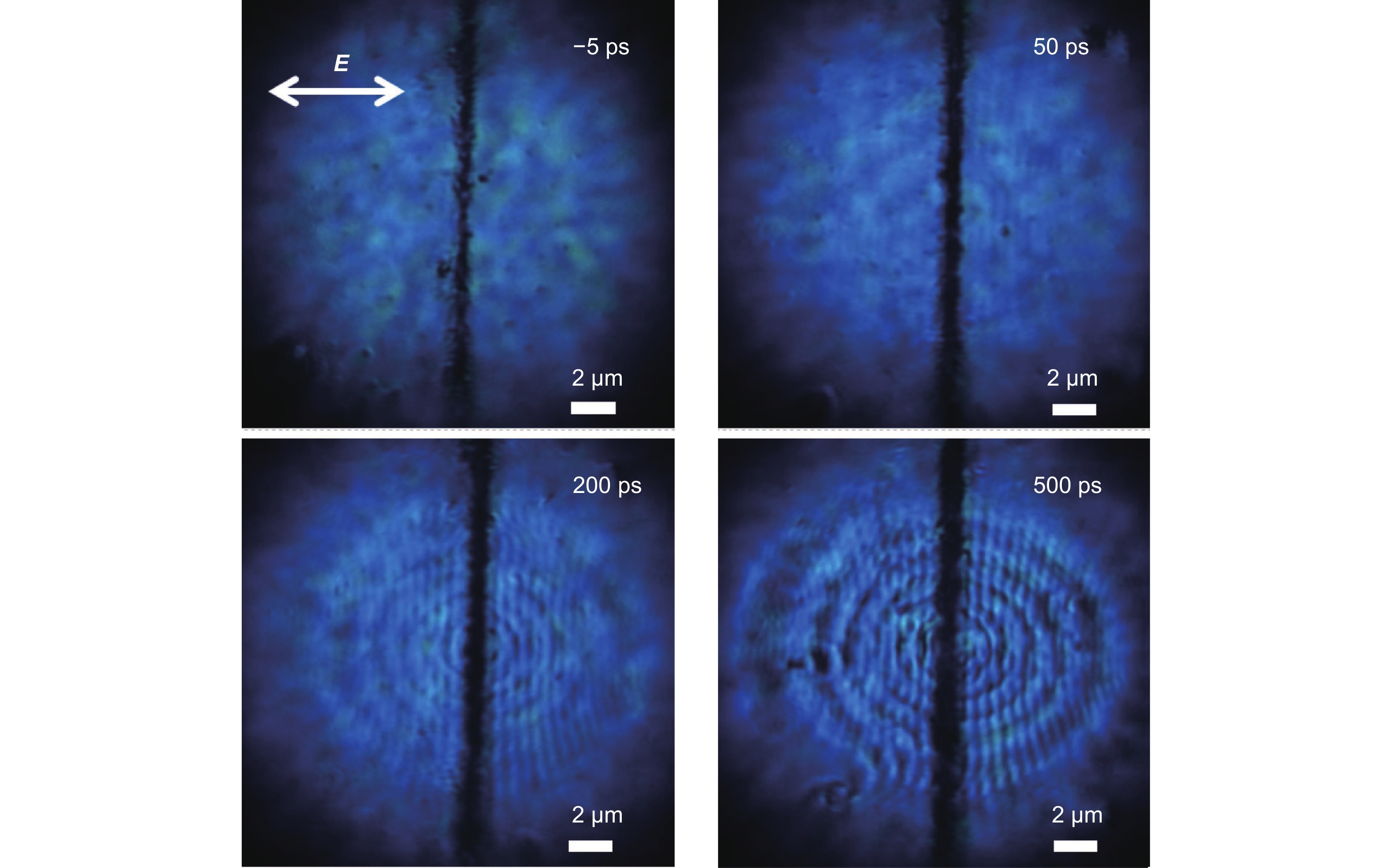
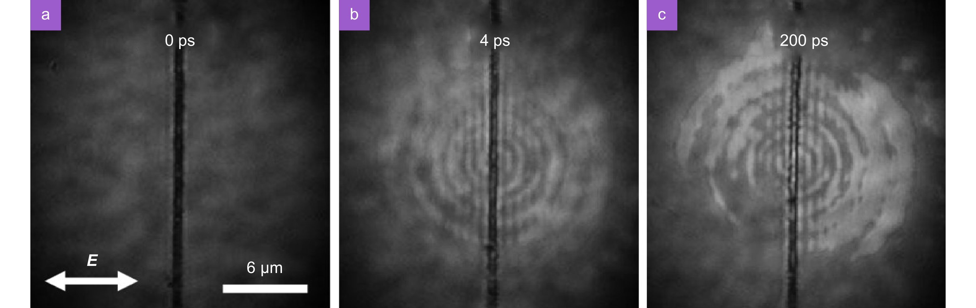
Figure 5 shows the optical microscope (OM) images of the transient LSFLs on the Si surface at different delay times52. The LSFL period was 680 ± 15 nm, and the direction was parallel to the nanogroove. The annular structures were caused by the diffraction effect of the concave lens. Surprisingly, periodic ripples quickly emerged. The transient ripples were clear at a delay time of 4.0 ps, which indicated that these ripples were due to surface melting, excluding other thermodynamics such as ablation and hydrodynamics. The AFM measurements further showed that the height fluctuation in the LSFL region was less than 0.6 nm, and had no spatial periodicity. The LSFL period was predicted based on the SPP model, and it coincided with the experimental results. The formation of LSFLs on silicon was due to the periodic energy deposition caused by the SPP excitation, rather than self-organization processes.
Scanning electron microscopy (SEM) and atomic force microscopy (AFM) are typically used to observe LIPSs. The resolutions of these methods are very high, however they cannot be used to study the dynamics of LIPS formation. Pump-probe spectroscopy is an effective method to study the kinetics of femtosecond laser ablation88. However, transient images of LIPSs cannot be observed directly19, 79. Therefore, we developed a collinear pump-probe imaging method to study the transient processes of LIPS formation25, 49, 52, 55, 56, 89. The spatial resolution is 300 nm and the temporal resolution is 0.6 ps. To show clearly the changes in the surface microstructure, the same spot was observed at three different times: before the arrival of the pump pulse, at the designed delay time, and after the ablation spot solidified.
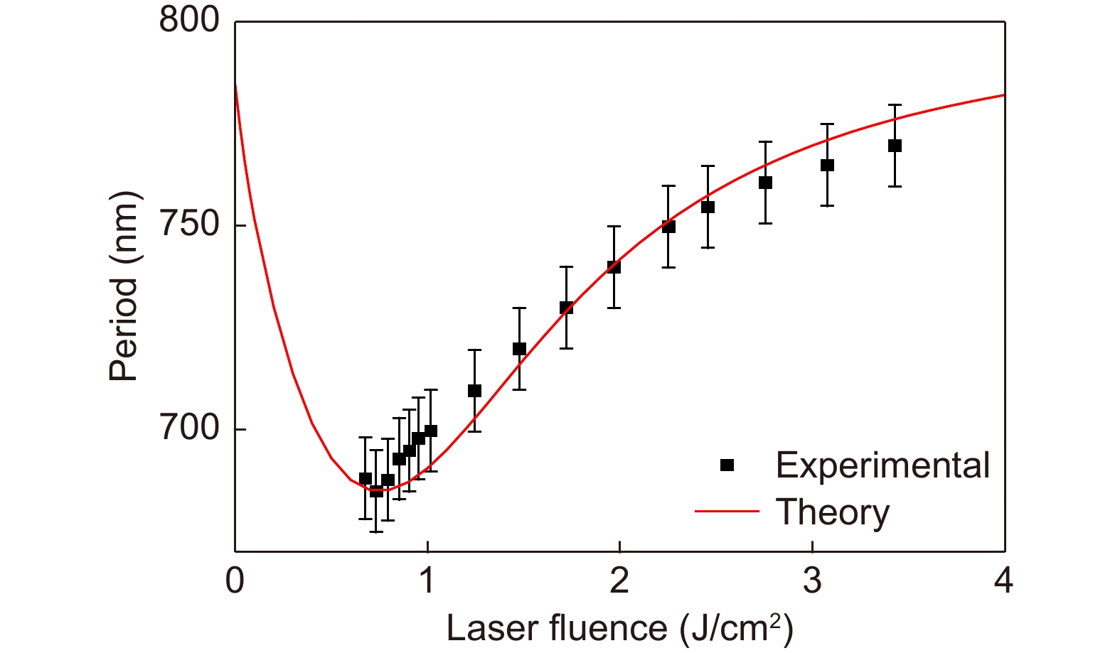
The dielectric constant is a key factor affecting the SPP wavelength21, 25. The dielectric constant in the ground state was usually used to study SPP on metal surfaces, which was an important factor that caused the deviation between the SPP theory and the experimental results. Therefore, Cheng et al. proposed and studied in detail the effects of hot electron localization and d-band transitions on the dielectric constant and SPP wavelength for gold at the highly excited states during femtosecond laser irradiation25. The LSFL period calculated by the developed SPP model decreased from 780 nm to 685 nm as the fluence increased to 0.75 J/cm2. However, as F was further increased to 2.5 J/cm2, the LSFL period increased to 756 nm. The developed SPP model accorded well with the experimental results, indicating that SPP excitation was the key during the formation of LSFLs on metal surfaces.
The pump-probe imaging experiments were further carried out to investigate the role of SPPs and thermal effects on the formation of LIPSs on noble-metal surfaces49. Under the irradiation of the second femtosecond laser pulse, transient periodic ripples were clearly observed on the gold film, but no obvious ripples remained after the surface solidified. The surface defects produced by the first laser pulse launched SPPs on the Au film, which caused further modulated energy deposition and induced transient LIPSs. However, because of the small electron–phonon coupling coefficient of Au, the slow heat process and strong melting effect caused the ripples to disappear. When the Au film was immersed in water, the LIPSs were retained because of the high cooling rate of the molten layers49. These experimental results indicated that the SPPs played an important role in the formation of LIPSs, while the thermal effect greatly influenced whether the transient ripples were retained after the molten surface solidified49 .
![Figure 7. LSFL periods as a function of laser fluence F. The black squares and error bars show the experimental data, and the red curve shows the theoretical values. Figure reproduced with permission from ref.25, American Physical Society.]()
LSFL periods as a function of laser fluence F. The black squares and error bars show the experimental data, and the red curve shows the theoretical values. Figure reproduced with permission from ref.25, American Physical Society.
The phenomena of femtosecond-LIPSs are very rich, and the formation mechanisms are very complicated. Are LIPSs caused by the periodic deposition of laser energy or by self-organization during laser excitation, melting, and solidification? The propagating SPP model has been widely accepted to explain the formation of LSFLs on semiconductor and metal surfaces, however several key issues remain to be addressed. First, the SPPs on the surfaces of gold and silver are very strong86, however it is difficult to form regular LSFLs on these noble metals10. Second, the periods of the LIPSs on metal surfaces are significantly smaller than the SPP wavelengths49, 87. The further development of new methods is required to solve these problems.
However, the period dependence of the LSFLs on metal surfaces was much different from the SPP model87, 90, 91. The SPP wavelengths were calculated by using the dielectric constants of silver, gold, copper, and aluminum in the ground states, which were significantly larger than the periods of LSFL ripples10, 49, 92. The d-band electrons in gold and silver could be excited to states above the Fermi surface93, 94. The free-electron density and plasma frequency both increased with laser fluence, resulting in longer SPP wavelengths. The LSFL periods were very different from those of the SPP model, which is a difficult problem to solve.
Noncollinear pump-probe imaging techniques have also been applied to observe the formation of LSFLs. Murphy et al. reported the formation of LSFLs on silicon irradiated with multiple pulses100. Using optical diffraction microscopy, Kafka et al. detected the formation of LSFLs on Cu films irradiated with a single femtosecond pulse54. Garcia-Lechuga et al. used a moving-spot multiple-pulse irradiation approach, and observed the birth and growth of individual ripples on a silicon surface101. It was demonstrated that the formation of LIPSs was initiated by free carrier generation, leading to non-thermal melting, liquid-phase overheating, and rapid solidification into the amorphous phase.
Figure 6 shows the evolution of the LSFLs formed on an Au film. The transient LSFLs began to appear at 45 ± 10 ps, and become more numerous and clearer over time25. Between 400 and 600 ps, the ripples appear to be the most distinct and regular. The ripples are perpendicular to the laser polarization with a period of 740 ± 10 nm.
The electronic band structures and optical properties of Ag and Ni are significantly different, and can represent noble and common metals, respectively. The dependence of the transient LSFL periods of Ag and Ni films on the laser fluence was studied using the collinear pump-probe imaging method56. The experimental results agreed well with the theoretical values based on the developed SPP theory. Thus, the developed SPP model explains the formation mechanism of LSFLs on different types of metal surfaces.
Figure 7 shows that the LSFL period increased from 685 nm to 770 nm when the fluence increased from 0.73 to 3.42 J/cm2 25, which was similar to the results for Si, GaP, and ZnO crystals51, 52, 98, 99. The SPP wavelength of gold was 780 nm for 800 nm light, which was significantly larger than the experimental value. With increasing laser fluence, free-electron density became larger, which led to longer SPP wavelength and LSFL period. Obviously, there is a great deviation between the SPP theory and the experimental results.
![Figure 6. Evolution of LSFLs formed on Au film irradiated by a single 800 nm laser pulse with a fluence of 1.96 J/cm2. The laser polarization, E, is perpendicular to the prefabricated nanogroove. Figure reproduced with permission from ref.25, American Physical Society.]()
Evolution of LSFLs formed on Au film irradiated by a single 800 nm laser pulse with a fluence of 1.96 J/cm2. The laser polarization, E, is perpendicular to the prefabricated nanogroove. Figure reproduced with permission from ref.25, American Physical Society.
![Figure 5. OM images of silicon surface irradiated by a single 800 nm femtosecond pulse of 0.18 J/cm2. The double arrows in (a) show the laser polarization direction. Figure reproduced with permission from ref.52, Optica Publishing Group, under the Optica Open Access Publishing Agreement.]()
OM images of silicon surface irradiated by a single 800 nm femtosecond pulse of 0.18 J/cm2. The double arrows in (a) show the laser polarization direction. Figure reproduced with permission from ref.52, Optica Publishing Group, under the Optica Open Access Publishing Agreement.
LSFLs are typically induced by multiple laser pulses. The material at the laser focus is partially ablated after each laser pulse irradiation, which makes the formation mechanisms more difficult to understand because of the effects of the scattered light and grating coupling feedback. Therefore, theoretical and experimental studies on the LSFLs induced by a single femtosecond laser pulse provide fundamental information on the origin of LSFLs on metal surfaces52, 95-97.
Efficient fabrication of high-quality LIPSs with shaped ultrafast laser pulses
Temporally shaped ultrafast laser-induced high-quality LIPSs
The fabrication efficiency, depth, and regularity of the LSFLs when using shaped pulses of 16.2 ps were significantly better than those using Gaussian femtosecond laser pulses8. The scan velocity for fabricating regular LSFLs was 2.3 times faster, while the LSFLs depth was 2 times deeper, and the diffraction efficiency was 3 times higher than that of LSFLs using Gaussian femtosecond laser pulses.
By controlling the voltage of each element of the spatial light modulator (SLM) via computer programming, the phase and/or amplitude of the laser spectrum can be modulated, and the 4f zero-dispersion pulse-shaping system can generate shaped laser pulses with arbitrary temporal distributions8. Specifically, the number of subpulses, interval between adjacent subpulses, and pulse energy of each subpulse can be flexibly adjusted.
Regular LSFLs on silicon were processed using a 4f configuration zero-dispersion pulse-shaping system8. A Gaussian pulse is shaped into pulse trains with an interval of 16.2 ps by using periodic π-phase step modulation. The transient LIPSs started appearing on the Si surface at a delay time of 4 ps52, which was shorter than the interval between adjacent sub-pulses. Thus, the transient LIPSs have started to appear under the illumination of the two main subpulses. When the subsequent subpulse reached the sample surface, the transient LIPSs induced by the previous subpulses enhanced the excitation of the SPPs, as well as the periodic distribution of the laser field.
Double temporally delayed femtosecond laser beams can efficiently induce uniform LSFLs in semiconductors, metals and dielectrics105, 106. A femtosecond laser was further shaped into symmetrical three- and four-pulse sequences for the fabrication of double-grating structures and HSFLs on fused silica107.
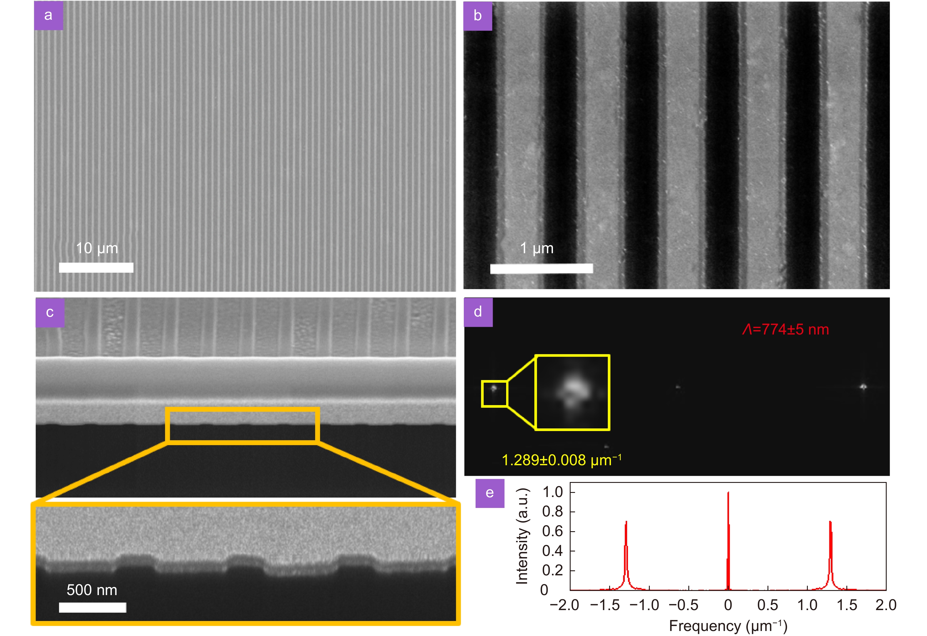
![Figure 8. (a–b) SEM pictures of LSFLs induced by the shaped pulse trains with an interval of 16.2 ps. (c) The cross section of LSFLs. (d) The 2D fast Fourier transform of (b). (e) Spectra of the 2D Fourier transform along the x-axis. Figure reproduced with permission from ref.8, Optica Publishing Group, under the Optica Open Access Publishing Agreement.]()
(a–b) SEM pictures of LSFLs induced by the shaped pulse trains with an interval of 16.2 ps. (c) The cross section of LSFLs. (d) The 2D fast Fourier transform of (b). (e) Spectra of the 2D Fourier transform along the x-axis. Figure reproduced with permission from ref.8, Optica Publishing Group, under the Optica Open Access Publishing Agreement.
When the subsequent small sub-pulses reached, the surface layer remained at a very high temperature. It was further excited and partially ablated, taking away some of the remaining heat (ablative cooling effect). Moreover, the ablated plume was further excited by the subsequent subpulses, and the debris was further ionized and vaporized, resulting in fewer deposited particles. Therefore, regular and uniform LSFLs were induced on the Si surface using a shaped pulse of 16.2 ps8, as shown in Fig. 8.
To efficiently fabricate uniform and regular LIPSs, three main challenges should be addressed: enhancement of periodic deposition of laser energy, reduction of residual heat, and avoidance of debris deposited on the ablation spots8. A temporally shaped ultrafast laser is an efficient tool for fabricating regular LIPSs102. By changing the sub-pulse interval, pulse number, and sub-pulse energy distribution of the burst pulse train, the regularity and uniformity of LIPSs were obviously improved, and the structural color was more vivid103, 104.
Spatially shaped femtosecond laser-induced LIPSs with high efficiency
Lin et al. developed a correction method for the spatial distortion and light intensity, which could greatly improve the accuracy of the spatial pattern and uniformity of the light intensity simply by changing the phase map loaded on the SLM112. This method was used to efficiently process colorful two-dimensional codes on silicon and shark-skin-like structures with superhydrophobic properties on stainless steel112, 113.
Maskless flexible spatial shaping based on spatiotemporal interference can modulate the interference intensity distribution into arbitrary patterns111. It was verified using a Michelson interferometer, where the phase of one laser beam was controlled via SLM.
Arbitrary spatial intensity distribution of femtosecond laser pulses can be modulated by loading a computer-generated hologram (CGH) on a SLM, and LIPSs can be processed in parallel with high efficiency108. For example, Hayasaki et al. successfully realized the parallel processing of microstructures by loading a mixed-phase Fresnel lens on the SLM109, 110.
The laser focal point of a cylindrical lens is only a few to tens of micrometers wide, while its length is on the order of 1–10 mm114, 115. Compared with ordinary circular lenses, the efficiency of femtosecond-LIPSs can be improved by a factor of 103–104 by using cylindrical lenses, which have been demonstrated in materials such as silicon and graphene oxide11, 57, 116-118. This method is very simple, and has important implications for the industrial application of femtosecond-LIPSs in the future.
Polarization shaped femtosecond-LIPSs
By using a liquid crystal SLM and/or Q-plate, a femtosecond Gaussian laser beam could be modulated into vortex light, radially polarized or angularly polarized beam119-122, and used to directly fabricate complex LIPS patterns77, 121-129. Two laser beams with s and p polarizations were collinearly focused on the SiC surface, and nanostructures with different morphologies were fabricated by adjusting the energy ratio of these two laser beams77. Radially and angularly polarized femtosecond lasers were focused on transparent materials and HSFL patterns consistent with the polarization distribution were fabricated125.
Efficient fabrication of complex femtosecond-LIPS patterns by multi-beam interference
Two-beam femtosecond laser interference was used to fabricate grating structures. By changing the laser polarization direction, interesting complex periodic structures covered with LIPSs have been efficiently fabricated130, 132. Recently, large-area regular LSFLs were efficiently fabricated on a silicon wafer using double-beam femtosecond laser interference focused by cylindrical lens. The space of the double-beam interference fringes was an integer multiple of the SPP wavelength, thereby effectively exciting the resonance-enhanced SPPs. The fabricated nanogratings were very regular, uniform, and smooth, and the resolution of the diffraction light was almost the same as that with commercial gold gratings57. Using a similar method, a large area of regular and uniform LIPSs was processed on the surface of quartz glass118.
![Figure 9. SEM images of composite LIPSs prepared by three-beam interference. The insets show the polarization combinations of the three laser beams. Figure reproduced with permission from ref.37, under a Creative Commons Attribution 4.0 International License.]()
SEM images of composite LIPSs prepared by three-beam interference. The insets show the polarization combinations of the three laser beams. Figure reproduced with permission from ref.37, under a Creative Commons Attribution 4.0 International License.
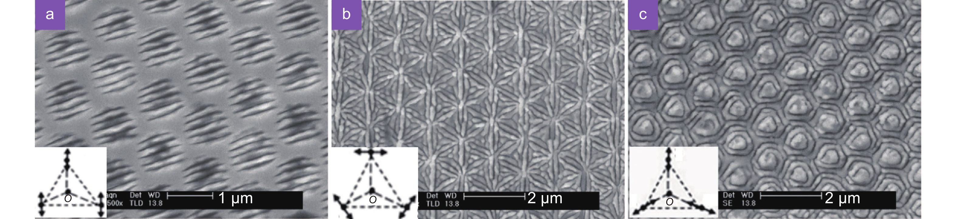
A wide variety of composite LIPSs such as hexagonally distributed nanogratings, hexagonal nanoflowers, and nanorings were efficiently fabricated on wide-bandgap SiC and ZnO semiconductors by changing the polarization combination of the three beams37, 131, as shown in Fig. 9. The four-beam interference method was further developed, and composite LIPSs such as square nanostructures, symmetric petal structures, and asymmetric helix-like structures were prepared on the surface of a ZnO crystal133.
Multibeam interference is an efficient etching technology for processing regular periodic patterns, where the light intensity distribution in the interference field is usually imprinted on the materials. By combining laser interference technology with femtosecond-LIPSs, many complex LIPS patterns were fabricated with high efficiency and quality by simultaneously controlling the light intensity distribution and polarization distribution37, 130. Experimental and theoretical results showed that the longer-period structure was determined by the intensity distribution, whereas the LIPS pattern was determined by the polarization distribution131.
Femtosecond laser direct writing of <100 nm nanostructures
Because of the diffraction limit, the size of the laser focus is typically a few hundred nanometers. The resolution of laser processing with high numerical aperture objectives is also on the order of hundreds of nanometers. The groove widths of HSFLs on semiconductor, dielectric, and metal surfaces induced by a femtosecond laser are typically less than 50 nm and less than 1/10 of the laser wavelength, opening up new avenues for laser processing with feature sizes smaller than 100 nm134-138. Liao et al. reported a single nanohollow channel with a width of 40 nm in porous glass using femtosecond laser-induced HSFL technology. It was used in nanofluidics in the field of single-molecule detection and biochip preparation. By precisely controlling the laser focus, fluences, and scanning speed, straight nanogrooves with widths smaller than 100 nm were prepared on the surfaces of fused silica and sapphire crystals135.
By controlling the laser polarization always perpendicular to the scanning direction, curved nanogrooves with widths smaller than 20 nm and curvature radii smaller than 100 nm were fabricated on a silicon surface139. Lin et al. processed curved nanogrooves with a feature size of 12 nm on silicon surfaces using 800 nm femtosecond laser direct writing with orthogonally polarized dual beams27.
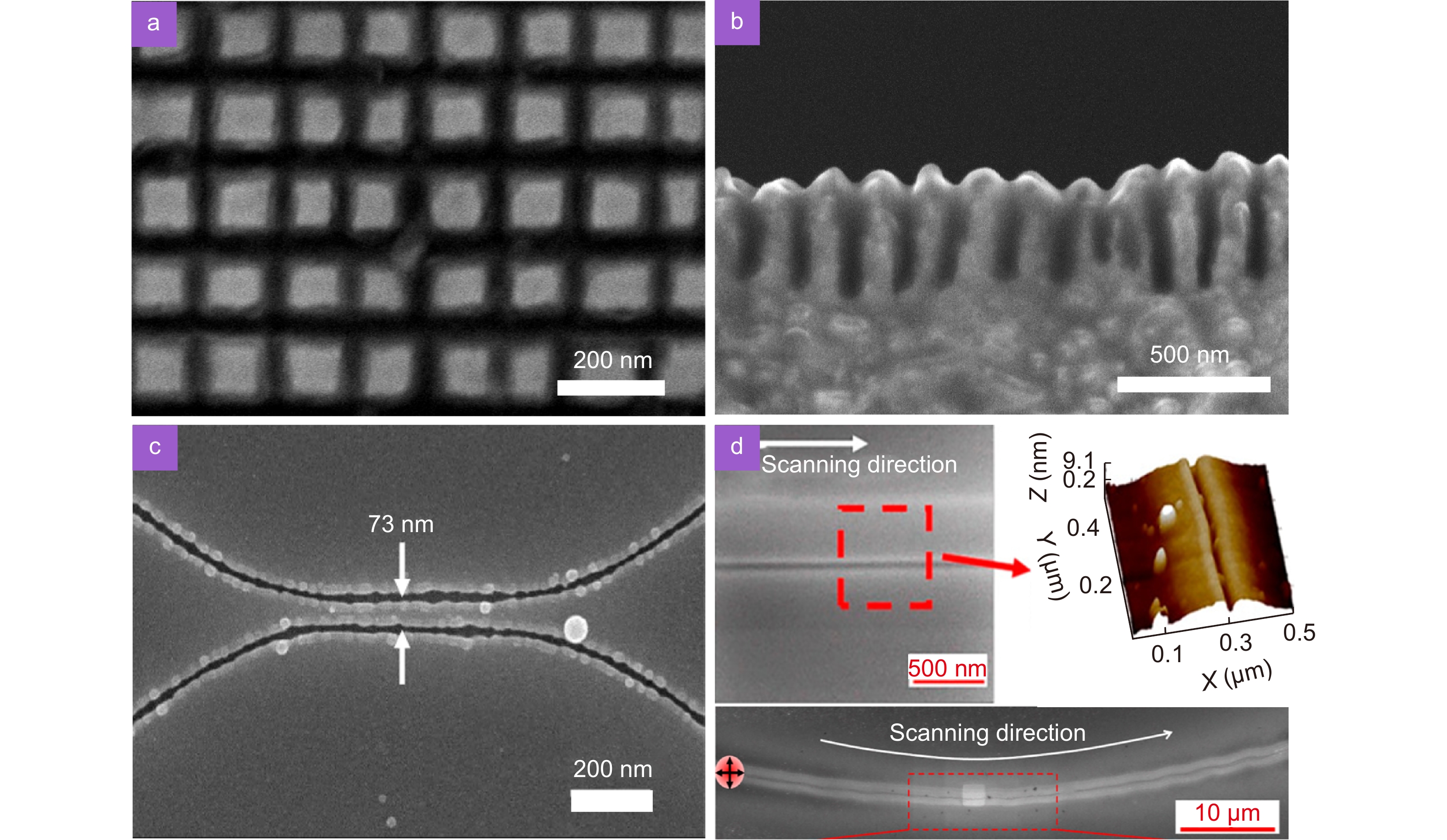
![Figure 10. (a) SEM images of nanosquares , and (b) the cross section of nanogratings . (c) Curvature and separation control of nanogrooves fabricated by 800 nm femtosecond laser with polarization control. (d) SEM and AFM images of curved single nanogroove on silicon surface induced by 800 nm femtosecond laser with orthogonally polarized dual beams. Figure reproduced with permission from: (a, b) ref.136, under Optica Open Access Publishing Agreement; (c) ref.139, under a Creative Commons Attribution 4.0 International License; (d) ref.27, American Chemical Society.]()
(a) SEM images of nanosquares , and (b) the cross section of nanogratings . (c) Curvature and separation control of nanogrooves fabricated by 800 nm femtosecond laser with polarization control. (d) SEM and AFM images of curved single nanogroove on silicon surface induced by 800 nm femtosecond laser with orthogonally polarized dual beams. Figure reproduced with permission from: (a, b) ref.136, under Optica Open Access Publishing Agreement; (c) ref.139, under a Creative Commons Attribution 4.0 International License; (d) ref.27, American Chemical Society.
A single nanogroove with a width of 30 nm and a double-groove structure with an interval of 150 nm were fabricated on a ZnO crystal surface immersed in water by precisely controlling the 800-nm femtosecond laser fluence and scanning speed136, as shown in Fig. 10. Double-groove grating structures and single-groove grating structures with different spacings were fabricated, with groove depths ranging from 200 to 300 nm and groove widths smaller than 40 nm. Nanosquare structures with dimensions of 150 nm × 150 nm and 150 nm × 250 nm were fabricated by direct writing twice along the vertical direction.
Applications of LIPSs
Femtosecond-LIPSs provide a mask-free, high-efficiency processing method for tuning material properties. This method has been used in many fields, with applications that include structural colors8, 32, 35, birefringent optical components34, 36, 38, optical absorption and luminescence33, 37, 39, and electrical properties40.
Structural colors
Structural colors originate from the interference, diffraction, or scattering produced by micro/nanostructures on the surface of a material32. LIPSs have been widely used to produce structural colors on metals, semiconductors and transparent materials8, 35, 118, 140-151.
The properties of such structural colors are determined by the period, depth, and orientation of the LIPSs. LIPSs with periods in the range of 400–
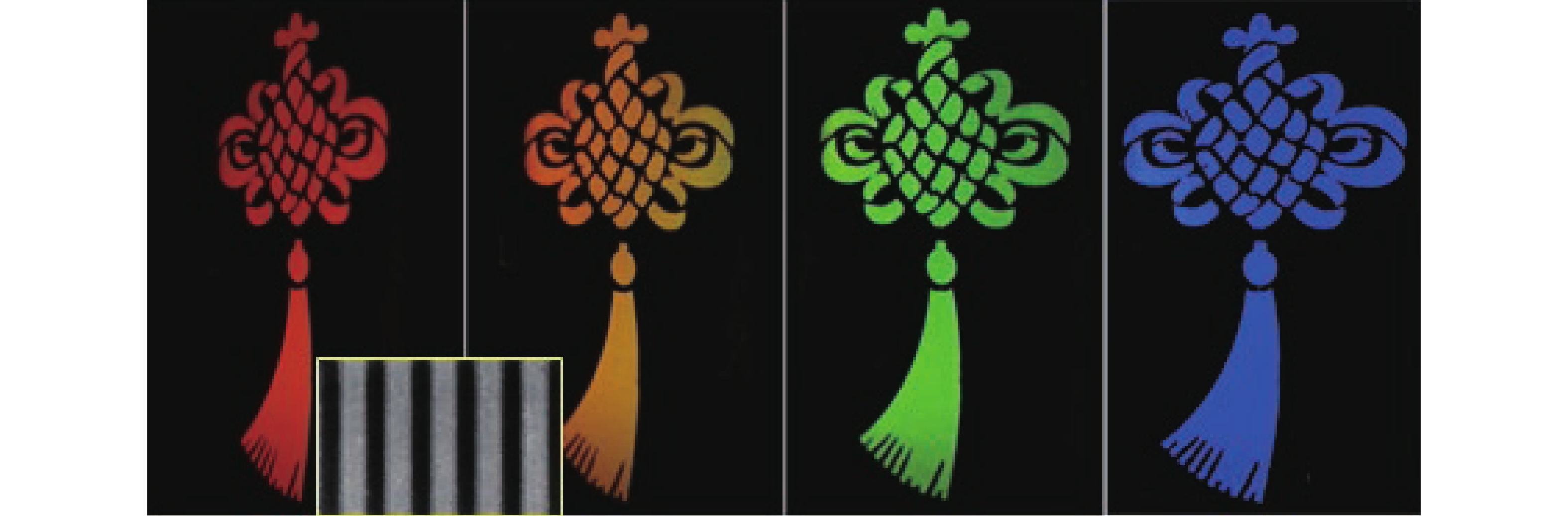
1500 nm were prepared on the surface of stainless steel using femtosecond lasers with different wavelengths140. These LIPSs demonstrated completely different colors under each diffraction order, such that the structural color of the stainless steel surface could cover most of the color gamut. The same LIPSs displayed different colors at different angles118, 142, 148. Therefore, surfaces with different colors were prepared by controlling the orientation of the LIPSs. Liu et al. proposed to control the orientation of LIPSs in real time using a femtosecond laser double-pulse sequence with orthogonal polarization and equal pulse energy and fabricated LIPSs with arbitrary orientations on silicon surfaces that were not affected by the scanning path147. This is of great significance for multi-layer encryption, anti-counterfeiting, and so on.The brightness and purity of the structural colors were affected by the regularity and depth of the LIPSs. The high-efficiency preparation of high-quality LIPSs has attracted increasing attention. Zhang et al.8 fabricated very regular and deep LSFLs on a silicon surface using temporally shaped pulses via a 4f zero-dispersion system and demonstrated very bright and pure structural colors, as shown in Fig. 11. Vivid structural colors on fused silica surfaces were prepared with high efficiency using the double-beam interference of femtosecond laser focused by cylindrical lens118. Chemical etching-assisted LIPSs are also an effective method for producing bright structural colors148, 150.
![Figure 11. Structural colors of “Chinese knot” pattern made up of LSFLs fabricated by a shaped pulse of 16.2 ps on Si surface under different diffraction angles. The inset shows an SEM image of regular LSFLs. Figure reproduced with permission from ref.8, Optica Publishing Group, under the Optica Open Access Publishing Agreement.]()
Structural colors of “Chinese knot” pattern made up of LSFLs fabricated by a shaped pulse of 16.2 ps on Si surface under different diffraction angles. The inset shows an SEM image of regular LSFLs. Figure reproduced with permission from ref.8, Optica Publishing Group, under the Optica Open Access Publishing Agreement.
Birefringent optical components and information storage
![Figure 12. (a-c) Imaging of anisotropic nanostructures and 5D optical data storage in fused silica153, 155. (a) Image of the slow axis azimuth of voxels, where the pseudo-color represents the slow axis azimuth. (b) SEM image of the nanolamella-like structure after polishing and KOH etching. (c) The enlarged area in the dashed square in (b). (d) The birefringent images of data voxels of different layers in a 100-layer 5D optical data storage in fused silica after removing the background. Insets are enlargements of small region (10 μm × 10 μm). (e) Polar diagram of the measured retardance and azimuth of all voxels in (d). Figure reproduced with permission from: (a-c) ref.153, Optica Publishing Group, under the Optica Open Access Publishing Agreement; (d, e) ref.155, under a Creative Commons Attribution License.]()
(a-c) Imaging of anisotropic nanostructures and 5D optical data storage in fused silica153, 155. (a) Image of the slow axis azimuth of voxels, where the pseudo-color represents the slow axis azimuth. (b) SEM image of the nanolamella-like structure after polishing and KOH etching. (c) The enlarged area in the dashed square in (b). (d) The birefringent images of data voxels of different layers in a 100-layer 5D optical data storage in fused silica after removing the background. Insets are enlargements of small region (10 μm × 10 μm). (e) Polar diagram of the measured retardance and azimuth of all voxels in (d). Figure reproduced with permission from: (a-c) ref.153, Optica Publishing Group, under the Optica Open Access Publishing Agreement; (d, e) ref.155, under a Creative Commons Attribution License.
Mechanisms and applications based on femtosecond laser-induced birefringence have been extensively studied, including various polarization-sensitive elements70, 156-158 such as polarization beam splitters159, polarization diffraction gratings160, and polarization optical vortex rotation converters123. HSFLs fabricated in amorphous silicon161, 162, silicon carbide163 and indium tin oxide (ITO) thin films164, 165 exhibit birefringence effects two orders of magnitude higher than those of quartz glass, demonstrating that high-refractive-index materials can be used to fabricate birefringent elements. Large-area HSFLs have been efficiently fabricated on a glass surface coated with an ITO thin film using femtosecond laser direct writing focused via a cylindrical lens166. The optical retardation reached 44 nm, which was eight times that of the HSFLs processed directly on a bare glass surface.
HSFL nanostructures inside fused silica exhibit birefringence effects comparable to those of quartz crystals34, 36, 152, 153 and have been used in the storage of multi-dimensional data, as shown in Fig. 12. Zhang et al.154 demonstrated that HSFLs could encode the intensity and polarization state of light at multiple levels and successfully retrieved digital files that were optically encrypted into five dimensions. Experiments indicated that HSFLs in silica glass have high stability and rewritability, meeting some requirements for developing high-density data storage38. Recently, Wang et al. demonstrated 100-layer 5D optical data storage based on femtosecond laser-induced birefringence with a high readout accuracy and no bit error rates155 , as shown in Fig. 12. At present, the limitations of optical storage technology lie mainly in efficient writing and fast and accurate reading. The writing speed has been increased to 225 kB/s153-155, which is mainly a result of the higher laser power and repetition frequency with pulse energy modulation, as shown in Fig. 12.
Enhancement of optical absorption and photoluminescence
The optical properties were significantly tuned after forming complex micro-nanostructures covered with LIPSs on the surfaces of metals, semiconductors, and dielectrics33, 35, 37, 39, 118, 167-174. “Black” silicon has been extensively studied and was shown to exhibit ultra-low reflectivity and very high absorption in the UV–NIR region as a result of nanostructures fabricated by femtosecond lasers33, 39, 171, 172.
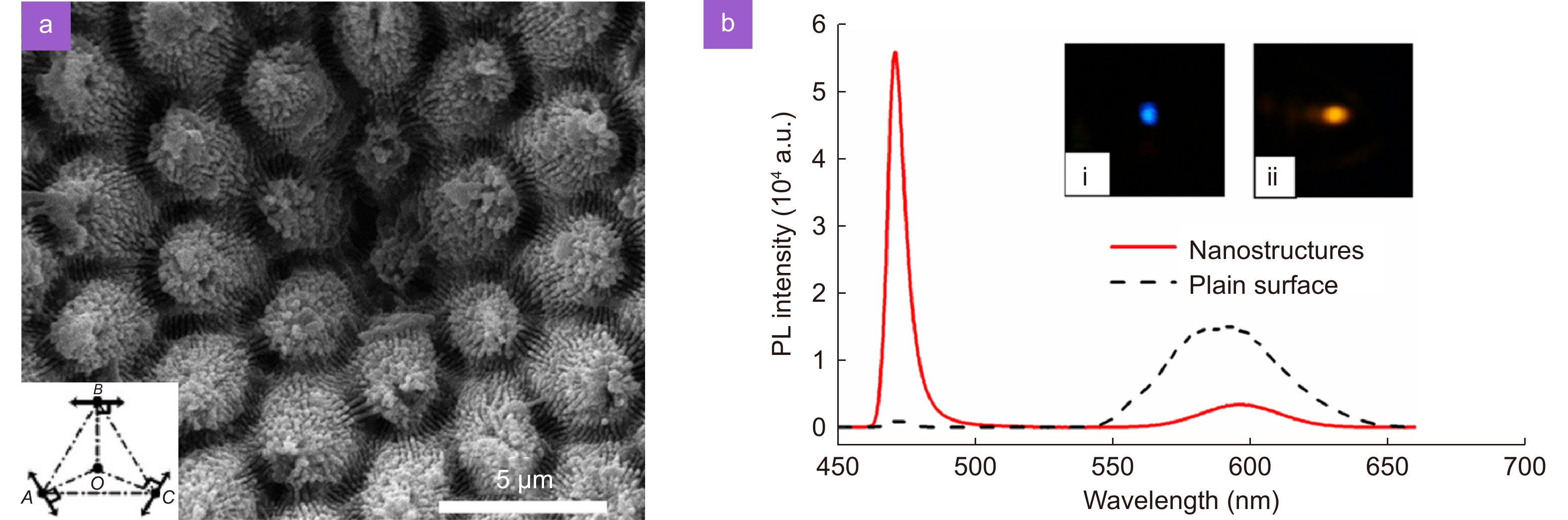
![Figure 13. (a) SEM image of composite nanostructures on ZnSe crystal. (b) The photoluminescence (PL) spectra of the plane surface and composite nanostructures irradiated by 1200 nm femtosecond laser. Insets (i) and (ii) show PL images of the nanostructures and plane surface, respectively. Figure reproduced with permission from ref.175, AIP Publishing.]()
(a) SEM image of composite nanostructures on ZnSe crystal. (b) The photoluminescence (PL) spectra of the plane surface and composite nanostructures irradiated by
1200 nm femtosecond laser. Insets (i) and (ii) show PL images of the nanostructures and plane surface, respectively. Figure reproduced with permission from ref.175, AIP Publishing.Various composite LIPSs have been efficiently fabricated on wide-bandgap SiC and ZnO semiconductors by the multi-beam interference of femtosecond lasers174, 176. These composite nanostructures exhibited greatly enhanced light absorption in the UV–NIR region, as well as an intense blue emission when excited by infrared femtosecond lasers. Compared with the smooth surface of ZnSe crystals, the blue light intensity of the composite nanostructures excited by a
1200 nm femtosecond laser was enhanced by 30–100 times175, as shown in Fig. 13.Electrical properties improved by LIPSs
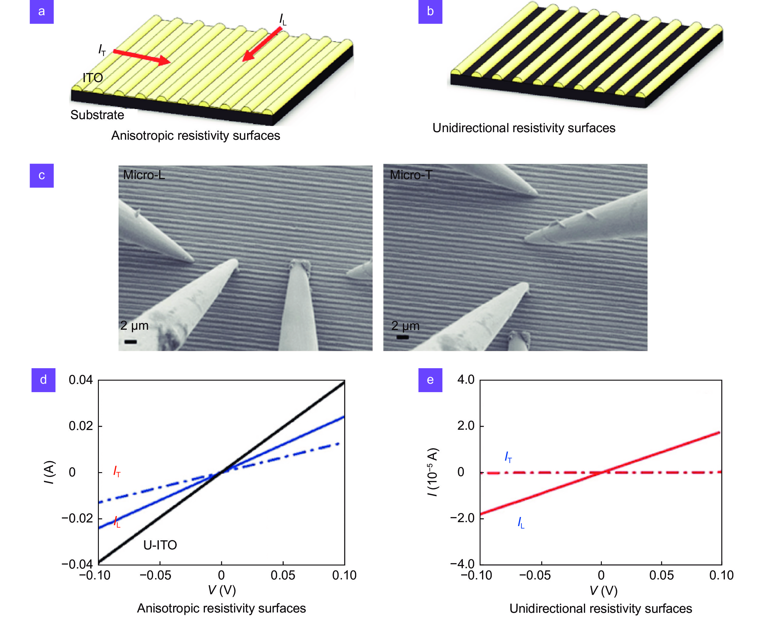
Recently, the effect of LIPSs on the electrical properties of ITO40, 41, 177 and the superconducting material niobium178, 179 has received increasing attention. ITO films are widely used as transparent conductive materials in solar cells, sensors, and displays. An ITO film with LIPSs exhibited good anisotropic conductivity and, if fabricated under appropriate conditions, could even achieve unidirectional conductivity, as shown in Fig. 1441. Moreover, the transmittance in the near-infrared region was greatly enhanced40, 41, 177. These results demonstrate the potentials of femtosecond LIPSs for efficiently fabricating large-scale transparent nanowires180.
Cubero et al.178, 179 analyzed the effect of laser irradiation on the critical current value of superconductors by measuring hysteresis loops, and proved that LIPSs could change the superconducting properties of niobium. The secondary electron emission from a copper surface with LIPSs was effectively reduced181, which was very effective in suppressing secondary electron emission in accelerators.
![Figure 14. (a–b) Schematic illustrations of the laser-induced structure in the ITO thin film on the substrate, and the resistivity measured longitudinally (IL) or transversely (IT) along the LIPS direction. (c) Microscopic configuration of the four-point probe measurement with the probes longitudinal (Micro-L) or transverse (Micro-T) aligned with the LIPSs. (d) and (e) are the I-V curves of the anisotropic resistivity surface and the unidirectional resistivity surface measured by the Micro-L or Micro-T method, respectively. Figure reproduced with permission from ref.41, under a Creative Commons Attribution License.]()
(a–b) Schematic illustrations of the laser-induced structure in the ITO thin film on the substrate, and the resistivity measured longitudinally (IL) or transversely (IT) along the LIPS direction. (c) Microscopic configuration of the four-point probe measurement with the probes longitudinal (Micro-L) or transverse (Micro-T) aligned with the LIPSs. (d) and (e) are the I-V curves of the anisotropic resistivity surface and the unidirectional resistivity surface measured by the Micro-L or Micro-T method, respectively. Figure reproduced with permission from ref.41, under a Creative Commons Attribution License.
Other applications
After femtosecond laser processing, the entire ablation area is covered with nanostructures, which can effectively increase the surface roughness and reduce the contact area with the droplet. This is an efficient method to alter the hydrophilicity and hydrophobicity of sample surfaces, and has been successfully demonstrated on various materials including metals, semiconductors, dielectrics, and polymers182-192.
Femtosecond-LIPSs were optimized on steel, titanium alloy, and atomic layer deposition cemented carbide surfaces. The friction coefficient and the wear were reduced significantly, which revealed the great potential for tribological applications193-199.
Outlook
In this paper, the formation mechanisms, high-quality and high-efficiency processing methods, and applications of LIPSs were reviewed. We believe that the following problems that may be worth further investigation.
Formation mechanisms of LIPSs
HSFLs are typically formed after irradiation with multiple pulses. Their formation mechanism is more complex and difficult to determine than that of LSFLs, requiring extensive experimental and theoretical studies, including numerical simulations of the dynamics using the COMSOL and FDTD methods. In recent years, various far-field super-resolution imaging methods have been reported200-202. Combining the pump-probe method with far-field super-resolution imaging is very interesting and may be helpful in revealing the formation mechanism of HSFLs irradiated by a femtosecond laser.
The formation mechanism of LIPSs has always been a hot topic in this field. The scattered light model and propagating SPP model are continuously being developed and refined and have been used to explain the formation of LSFLs on dielectrics, semiconductors, and metals. However, the formation mechanism of LSFLs requires further experimental and theoretical studies, especially ultrafast dynamics.
Patterns with features of <30 nm obtained by direct writing
The groove width of HSFLs is only tens of nanometers, which provides a new method of nanofabrication using ultrafast laser direct writing. However, before this can be widely applied, there are still many problems to be solved such as the slow scanning speed and poor uniformity of the nanogrooves. In the last decade, multi-dimensional laser shaping technologies in time/frequency and polarization have been rapidly developed108, 203. Synchronizing laser direct writing and multi-dimensional laser shaping in real time will ensure that the nanogrooves grow along the direction of the direct laser writing, improve the local optical field enhancement, and reduce the residual heat of ablation. This is expected to efficiently fabricate high-quality nanopatterns with features less than 30 nm.
LIPSs based on multi-dimensional laser shaping and its applications
Large-area LIPSs fabricated with high quality, efficiency, and stability can greatly promote their applications in many fields. By developing pulse-shaping methods based on the 4f configuration zero-dispersion system or Fabry-Perot interferometer204, the regularity and depth of LIPSs can be effectively improved, which will improve the phase retardation and writing speed and reduce the bit error rate when reading out. Combining time/frequency shaping and spatial shaping can improve the regularity and depth of LIPSs fabricated with high efficiency, thereby improving the purity and brightness of the structural colors. By simultaneously controlling the polarization and spatial distribution of the laser field, nanostructures with designed patterns and specific nanogroove distributions can be processed with high efficiency. Combining time/frequency domain shaping and polarization shaping can improve the quality and efficiency of far-field nanofabrication and allow LIPS applications in new fields such as metasurfaces and microelectronics.
Acknowledgements
This work was supported by the National Natural Science Foundation of China (12074123, 11804227, 91950112), and the Ministry of Science and Technology of China (Grant No. 2021YFA1401100), and the Foundation of ‘Manufacturing beyond limits’ of Shanghai. The English text of this manuscript was edited using the OSA Language Editing Services (http://languageediting.osa.org/).
Competing interests
The authors declare no competing financial interests.
-
References
[1] Fork RL, Greene BI, Shank CV. Generation of optical pulses shorter than 0.1 psec by colliding pulse mode locking. Appl Phys Lett 38, 671–672 (1981).
DOI: 10.1063/1.92500[2] Chichkov BN, Momma C, Nolte S, Von Alvensleben F, Tünnermann A. Femtosecond, picosecond and nanosecond laser ablation of solids. Appl Phys A 63, 109–115 (1996).
DOI: 10.1007/BF01567637[3] Sugioka K, Cheng Y. Ultrafast lasers—reliable tools for advanced materials processing. Light Sci Appl 3, e149 (2014).
DOI: 10.1038/lsa.2014.30[4] Buividas R, Mikutis M, Juodkazis S. Surface and bulk structuring of materials by ripples with long and short laser pulses: recent advances. Prog Quant Electron 38, 119–156 (2014).
DOI: 10.1016/j.pquantelec.2014.03.002[5] Yang QX, Liu HL, He S, Tian QY, Xu B et al. Circular cladding waveguides in Pr:YAG fabricated by femtosecond laser inscription: Raman, luminescence properties and guiding performance. Opto-Electron Adv 4, 200005 (2021).
DOI: 10.29026/oea.2021.200005[6] Wang HT, Hao CL, Lin H, Wang YT, Lan T et al. Generation of super-resolved optical needle and multifocal array using graphene oxide metalenses. Opto-Electron Adv 4, 200031 (2021).
View full references list -
Cited by
Periodical cited type(67)
1. Dong, B., Sun, Q., Wang, J. et al. Defect evolution and color center generation of high energy density femtosecond laser processed IIa diamond. Nanotechnology and Precision Engineering, 2025, 8(4): 043004. DOI:10.1063/10.0036174 2. Guan, Y., Ding, Y., Fang, Y. et al. Far-field femtosecond laser-driven λ/73 super-resolution fabrication of 2D van der Waals NbOI2 nanostructures in ambient air. Nature Communications, 2025, 16(1): 4149. DOI:10.1038/s41467-025-59520-9 3. Sun, X., Wang, W., Zhang, C. et al. Fabrication of color code by femtosecond laser-induced nanostructures on the surface of metal films with yttria-stabilized zirconia substrate. Optics Communications, 2025. DOI:10.1016/j.optcom.2025.132151 4. Sun, X., Wang, W., Mei, X. et al. Comparison of different methods for generating structural colors on polymer surface using femtosecond laser. Optics and Laser Technology, 2025. DOI:10.1016/j.optlastec.2025.113029 5. Liu, X., Huang, C., Liu, H. et al. The evolution mechanism of femtosecond laser-induced periodic structure on monocrystalline silicon with scanning rate and the associated material rearrangement process. Materials Science in Semiconductor Processing, 2025. DOI:10.1016/j.mssp.2025.109714 6. Ahmed, A.S., Sancio, D., Müller, D.W. et al. Femtosecond-DLIP on tin-alloyed bronze: Effect of pulse fluence on surface topography for antibacterial application. Materials Today Advances, 2025. DOI:10.1016/j.mtadv.2025.100596 7. Xu, L., Yan, W., Cui, W. et al. Repetition Frequency-Dependent Formation of Oxidized LIPSSs on Amorphous Silicon Films. Photonics, 2025, 12(7): 667. DOI:10.3390/photonics12070667 8. Liao, J., Zhang, D., Li, Z. Conceptional Pure-Tungsten Metasurfaces Based on Femtosecond Laser Nanomanufacturing. Engineering, 2025. DOI:10.1016/j.eng.2024.06.018 9. Fang, Y., Hao, H., Wang, Q. et al. Metasurface-generated Spin-multiplexed & Grafted Perfect Vector Vortex Beams for High-dimensional Optical Information Encryption. Laser and Photonics Reviews, 2025, 19(10): 2402033. DOI:10.1002/lpor.202402033 10. Wang, D., Lei, X., Li, K. et al. Enhancing the corrosion resistance of Zr alloy: Construction of wavy and coralline surface structures by femtosecond laser ablations in air and water. Surfaces and Interfaces, 2025. DOI:10.1016/j.surfin.2025.106483 11. Matei, A.T., Visan, A.I., Negut, I. Laser-Fabricated Micro/Nanostructures: Mechanisms, Fabrication Techniques, and Applications. Micromachines, 2025, 16(5): 573. DOI:10.3390/mi16050573 12. Zheng, N., Smith, D., Ng, S.H. et al. Infrared Absorption of Laser Patterned Sapphire Al2O3 for Radiative Cooling. Micromachines, 2025, 16(4): 476. DOI:10.3390/mi16040476 13. Hua, R., Xu, Z., Tao, Z. et al. Fabrication of high-quality surface microtextures on GaN by femtosecond laser direct writing. Nanotechnology and Precision Engineering, 2025, 8(1): 013005. DOI:10.1063/10.0028760 14. Ahmed, K., Agrawal, A.K., Kaushik, S. et al. Plasmonic waveguide-mode based aluminum nanogratings for enhanced chemical and biological sensing in the UV regime. Journal of Optics United Kingdom, 2025, 27(3): 035001. DOI:10.1088/2040-8986/adab03 15. Li, T., Tang, R., Xu, L. et al. Femtosecond Laser Ablation of High-Entropy Ceramics RE2(Ce0.2Zr0.2Hf0.2Sn0.2Ti0.2)2O7 (RE = Sm, Eu, Er) in Liquid for Colloid Synthesis. Journal of Physical Chemistry C, 2025, 129(7): 3707-3720. DOI:10.1021/acs.jpcc.4c04851 16. Yang, J., Zhou, S., Yang, M. et al. Antireflection microstructures on a ZnS surface fabricated by femtosecond laser direct writing assisted with wet etching. Optical Materials, 2025. DOI:10.1016/j.optmat.2024.116597 17. Ganeev, R.A., Yassine, A., Elnassar, Z. et al. 2D ripples and grooves formation on GaAs using different states of polarization of femtosecond pulses. Materials Science in Semiconductor Processing, 2025. DOI:10.1016/j.mssp.2024.109062 18. Li, Z., Chen, H., Han, M. et al. Femtosecond Laser-Induced Grid-Like Periodic Surface Structure on Silicon Substrate and Its Preliminary Application | [飞 秒 激 光 诱 导 硅 网 格 状 条 纹 结 构 及 其 初 步 应 用]. Zhongguo Jiguang Chinese Journal of Lasers, 2025, 52(4): 0402403. DOI:10.3788/CJL240884 19. Li, K., Han, R., Suo, M. et al. High quality nanogratings far beyond diffraction limits on silicon efficiently fabricated using femtosecond laser dual-beam interference direct writing. Optics and Laser Technology, 2025. DOI:10.1016/j.optlastec.2024.111505 20. Zhang, J., Han, B., Liu, Y. et al. Theoretical Study of Transient Properties for Laser-Induced Periodic Structures on Gold Surface | [激 光 诱 导 金 表 面 周 期 性 结 构 瞬 态 特 性 理 论 研 究]. Laser and Optoelectronics Progress, 2025, 62(1): 0114002. DOI:10.3788/LOP240826 21. Yang, Q., Yu, M., Chen, Z. et al. A novel approach towards robust construction of physical colors on lithium niobate crystal. Opto Electronic Advances, 2025, 8(3): 240193. DOI:10.29026/oea.2025.240193 22. Devi, N., Su, C.-R., Arpornwichanop, A. et al. Fabrication of superhydrophobic TiN-coated SS304 flow field plates via femtosecond laser processing for fuel cell applications. International Journal of Hydrogen Energy, 2024. DOI:10.1016/j.ijhydene.2024.11.165 23. Omeje, I.S., Iabbaden, D., Ganster, P. et al. Atomistic Simulations of Wetting Dynamics of Water Nanodroplets on Nanotextured Titanium: Implications for Medical Implants. ACS Applied Nano Materials, 2024, 7(21): 24426-24436. DOI:10.1021/acsanm.4c03946 24. Yin, J.-H., Cao, Y.-Z., Shang, Y.-Y. et al. Ablation mechanism and protection of aluminum alloy under high power laser irradiation: A review | [铝合金在高功率激光辐照下的烧蚀机理及损伤防护研究综述]. Journal of Central South University, 2024, 31(11): 4039-4059. DOI:10.1007/s11771-024-5811-4 25. Li, R., Liu, S., Zhou, Y. et al. Absorbing-coating-assisted laser-induced periodic surface structures on solids. Optics and Laser Technology, 2024. DOI:10.1016/j.optlastec.2024.110994 26. Kang, H.-B., Tang, W.-J., Jia, C.-L. et al. Optical and fluorescent properties in Er, Yb:YAG double-line waveguide by femtosecond laser direct writing. Physica B Condensed Matter, 2024. DOI:10.1016/j.physb.2024.416099 27. Wu, J.-P., Zhao, J., Xiao, G.-J. et al. Fabrication and characteristics of the planar and ridge Er3+-doped germanate glass waveguides. Journal of Materials Science Materials in Electronics, 2024, 35(24): 1637. DOI:10.1007/s10854-024-13413-7 28. Legrand, Q., Valette, S. Separation of the topographical and chemical components of the wettability of textured surfaces by femtosecond laser. Surfaces and Interfaces, 2024. DOI:10.1016/j.surfin.2024.104720 29. Kalnins, K., Kim, V.V., Reddy, A.N.K. et al. Spatially Variable Ripple and Groove Formation on Gallium Arsenide Using Linear, Radial, and Azimuthal Polarizations of Laser Beam. Photonics, 2024, 11(8): 710. DOI:10.3390/photonics11080710 30. Zheng, N., Buividas, R., Huang, H.-H. et al. Laser Machining at High ∼PW/cm2 Intensity and High Throughput. Photonics, 2024, 11(7): 598. DOI:10.3390/photonics11070598 31. Xia, Z., Zhang, J., Qian, J. et al. Equivalent power densities model for multi-pulse ultrashort pulsed laser processing. Applied Physics A Materials Science and Processing, 2024, 130(6): 440. DOI:10.1007/s00339-024-07571-y 32. Obata, K., Kawabata, S., Hanada, Y. et al. High performance micromachining of sapphire by laser induced plasma assisted ablation (LIPAA) using GHz burst mode femtosecond pulses. Opto Electronic Science, 2024, 3(6): 230053. DOI:10.29026/oes.2024.230053 33. Banerjee, D., Akkanaboina, M., Kanaka, R.K. et al. Nanotubular Arrayed LIPSS Achieved with Femtosecond Bessel Beam on Silver Surface for SERS-Based Multiple Explosive Sensing. Journal of Physical Chemistry C, 2024, 128(11): 4655-4665. DOI:10.1021/acs.jpcc.4c00160 34. Ren, Y., Guo, K., Li, Y. et al. Femtosecond laser induced periodic surface structures on crystals: Formation, evolution and application. Vacuum, 2024. DOI:10.1016/j.vacuum.2023.112900 35. Han, R., Zhang, Y., Jiang, Q. et al. Ultrafast dynamics of femtosecond laser-induced high spatial frequency periodic structures on silicon surfaces. Opto Electronic Science, 2024, 3(3): 230013. DOI:10.29026/oes.2024.230013 36. Geng, J., Yan, J., Shi, L. s-Polarized Laser Oblique Incidence Induces“Leaf Vein-Like” Self-Organizing Stripe Structures | [s 偏振激光斜入射诱导类“叶脉”状自组织条纹结构]. Laser and Optoelectronics Progress, 2024, 61(3): 0314001. DOI:10.3788/LOP232621 37. Liu, J., Zhang, H., Ai, S. et al. New channel guiding structures via femtosecond laser direct writing z-cut LiNbO3 crystals. Results in Physics, 2024. DOI:10.1016/j.rinp.2024.107379 38. Zhang, D., Chen, T., Shen, T. et al. Sub-diffraction limited nanogroove fabrication of 30 nm features on diamond films using 800 nm femtosecond laser irradiation. Heliyon, 2024, 10(2): e24240. DOI:10.1016/j.heliyon.2024.e24240 39. Guo, Y., Zhao, H. Femtosecond laser processed superhydrophobic surface. Journal of Manufacturing Processes, 2024. DOI:10.1016/j.jmapro.2023.12.005 40. Yulianto, N., Titok Sugiarto, I., Panji Tresna, W. et al. Laser-Induced Periodic Nanoripples Generation on Gallium Nitride Using Near-infrared Ultrashort Pulsed Laser. Journal of Physics Conference Series, 2024, 2696(1): 012002. DOI:10.1088/1742-6596/2696/1/012002 41. Dobrotvorskiy, S., Aleksenko, B.A., Basova, Y. et al. MECHANISM OF LIPSS FORMATION UNDER THE INFLUENCE OF PLASMA LENS DURING FEMTOSECOND LASER PROCESSING. International Journal of Mechatronics and Applied Mechanics, 2024, 2024(18): 7-17. DOI:10.17683/ijomam/issue18.1 42. Vanlallawmzuali, Lalbiaktluangi, C., Singh, A., Zothanpuia, Yadav, M.K. Surface modification: strategies to prevent microbial growth on medical implants. Microbial Biofilms Role in Human Infectious Diseases, 2024. DOI:10.1016/B978-0-443-19252-4.00008-0 43. Li, W., Wu, J., Li, Y. et al. Simulation study on the thermal effect of continuous laser heating quartz materials. Frontiers in Chemistry, 2024. DOI:10.3389/fchem.2024.1435562 44. [No author name available]. Microstructural and properties of ultrafast laser selective micro-welding joints of sapphire and Invar alloys | [蓝宝石与 Invar 合金超快激光选区微焊接接头组织和性能]. Hanjie Xuebao Transactions of the China Welding Institution, 2023, 44(12): 41-48 and 62. DOI:10.12073/j.hjxb.20230613012 45. Mincuzzi, G., Bourtereau, A., Gemini, L. et al. Through the Forming Process of Femtosecond-Laser Nanotextured Sheets for Production of Complex 3D Parts. Applied Sciences Switzerland, 2023, 13(22): 12500. DOI:10.3390/app132212500 46. Ni, J., Wei, Q., Zhang, Y. et al. Super-resolution three-dimensional structured illumination profilometry for in situ measurement of femtosecond laser ablation morphology. APL Photonics, 2023, 8(10): 101302. DOI:10.1063/5.0165363 47. Liu, Z., Yuan, Y., Li, Z. et al. Interaction Between Ultrafast Laser and Transparent Hard Materials: from Phase Change Mechanism to Eternal Optical Data Storage | [飞 秒 激 光 与 透 明 硬 质 材 料 的 相 互 作 用:从 相 变 机 理 到永 久 光 存 储]. Zhongguo Jiguang Chinese Journal of Lasers, 2023, 50(18): 1813005. DOI:10.3788/CJL230742 48. Daskalova, A., Angelova, L. Design of Surfaces with Persistent Antimicrobial Properties on Stainless Steel Developed Using Femtosecond Laser Texturing for Application in “High Traffic” Objects. Nanomaterials, 2023, 13(17): 2396. DOI:10.3390/nano13172396 49. Jia, Y., Chen, F. Recent progress on femtosecond laser micro-/nano-fabrication of functional photonic structures in dielectric crystals: A brief review and perspective. APL Photonics, 2023, 8(9): 090901. DOI:10.1063/5.0160067 50. Liu, Y., Zhu, X., Jin, C. et al. High-quality Subwavelength Grating Structures Fabrication on Fused Silica Surfaces by Femtosecond Laser | [融 石 英 表 面 高 质 量 亚 波 长 光 栅 结 构 的飞 秒 激 光 加 工]. Guangzi Xuebao Acta Photonica Sinica, 2023, 52(7): 0752307. DOI:10.3788/gzxb20235207.0752307 51. Shi, H., Yao, Q., Yin, W. et al. Study on Polarization Dependence of Ultrafast Combination Pulse Ablation on Silicon Surface(Invited) | [超 快 复 合 脉 冲 烧 蚀 硅 表 面 的 偏 振 依 赖 性 研 究(特 邀)]. Guangzi Xuebao Acta Photonica Sinica, 2023, 52(7): 0752304. DOI:10.3788/gzxb20235207.0752304 52. Shi, L., Geng, J., Qiu, M. Influence of Scanning Direction on the Quality of LIPSS on Metal-Si Hybrid Films(Invited) | [扫 描 方 向 对 金 属 和 硅 复 合 薄 膜 表 面 激 光 诱 导自 组 织 加 工 质 量 的 影 响(特 邀)]. Guangzi Xuebao Acta Photonica Sinica, 2023, 52(7): 0752303. DOI:10.3788/gzxb20235207.0752303 53. Rajendran, R., Krishnadev, E.R., Anoop, K.K. Direct Femtosecond Laser Processing for Generating High Spatial Frequency LIPSS (HSFL) on Borosilicate Glasses with Large-Area Coverage. Photonics, 2023, 10(7): 793. DOI:10.3390/photonics10070793 54. Li, P., Yin, R., Cheng, J. et al. Bacterial Biofilm Formation on Biomaterials and Approaches to Its Treatment and Prevention. International Journal of Molecular Sciences, 2023, 24(14): 11680. DOI:10.3390/ijms241411680 55. Bogatskaya, A., Gulina, Y., Smirnov, N. et al. An Experimental Study of Multiphoton Ionization in Fused Silica at IR and Visible Wavelengths. Photonics, 2023, 10(5): 515. DOI:10.3390/photonics10050515 56. Wang, C., Chen, X., Jia, X. et al. Fabrication of the double-layer millimeter wave frequency selective surface by femtosecond laser. Optik, 2023. DOI:10.1016/j.ijleo.2023.170726 57. Jiang, Q., Zhang, Y., Xu, Y. et al. Extremely High-Quality Periodic Structures on ITO Film Efficiently Fabricated by Femtosecond Pulse Train Output from a Frequency-Doubled Fabry–Perot Cavity. Nanomaterials, 2023, 13(9): 1510. DOI:10.3390/nano13091510 58. Banerjee, D., Akkanaboina, M., Kumar Kanaka, R. et al. Femtosecond Bessel beam induced ladder-like LIPSS on trimetallic surface for SERS-based sensing of Tetryl and PETN. Applied Surface Science, 2023. DOI:10.1016/j.apsusc.2023.156561 59. Lin, Y., Chen, S., Xu, C. et al. Femtosecond laser upgrading the quality of bismuth films to enhance ultra-broadband photodetection. Optics Express, 2023, 31(6): 9515-9525. DOI:10.1364/OE.482018 60. Yin, W., Song, J., Ren, X. et al. Nonlinear ionization control by temporally shaped fs+ps double-pulse sequence on ZnO. Chinese Optics Letters, 2023, 21(2): 021602. DOI:10.3788/COL202321.021602 61. Wu, Y., Xie, P., Ding, Q. et al. Magnetic plasmons in plasmonic nanostructures: An overview. Journal of Applied Physics, 2023, 133(3): 030902. DOI:10.1063/5.0131903 62. Geng, J., Shi, L., Liu, J. et al. Laser-induced deep-subwavelength periodic nanostructures with large-scale uniformity. Applied Physics Letters, 2023, 122(2): 021104. DOI:10.1063/5.0138290 63. Chen, Z., Yang, Q., Liu, H. Phase transition properties of the LIPSS induced by femtosecond laser direct writing on PMN-PT crystal | [飞秒激光直写诱导 PMN-PT 晶体表面 LIPSS 结构相变特性]. Guangdian Gongcheng Opto Electronic Engineering, 2023, 50(3): 220275. DOI:10.12086/oee.2023.220275 64. Cao, G., Lin, H., Jia, B. Broadband Diffractive Graphene Orbital Angular Momentum Metalens by Laser Nanoprinting. Ultrafast Science, 2023. DOI:10.34133/ultrafastscience.0018 65. Pimenov, S.M., Zavedeev, E.V., Arutyunyan, N.R. et al. Femtosecond laser-induced periodic surface structures on diamond-like nanocomposite films. Diamond and Related Materials, 2022. DOI:10.1016/j.diamond.2022.109517 66. Chen, L., Yang, J., Jiang, Q. et al. Regular Periodic Surface Structures on Indium Tin Oxide Film Efficiently Fabricated by Femtosecond Laser Direct Writing with a Cylindrical Lens. Materials, 2022, 15(15): 5092. DOI:10.3390/ma15155092 67. Tan, D., Sun, K., Li, Z. et al. Photo-processing of perovskites: current research status and challenges. Opto Electronic Science, 2022, 1(11) DOI:10.29026/oes.2022.220014 Other cited types(1)
-
Author Information
-
Copyright
Open Access. © The Author(s). This article is licensed under a Creative Commons Attribution 4.0 International License. To view a copy of this license, visit http://creativecommons.org/licenses/by/4.0/. -
About this Article
Cite this Article
Yuchan Zhang, Qilin Jiang, Mingquan Long, et al. Femtosecond laser-induced periodic structures: mechanisms, techniques, and applications. Opto-Electronic Science 1, 220005 (2022). DOI: 10.29026/oes.2022.220005Download CitationArticle History
- Received Date March 21, 2022
- Accepted Date May 09, 2022
- Published Date June 20, 2022
Article Metrics
Article Views(21322) PDF Downloads(1602)
 OE Journals Group

Reports the physical mechanisms and fundamental science of optics, photonics and optoelectronics
Open Access