E-mail Alert
 RSS
RSS-
Abstract
Optical antennas play an important role in optical field manipulation. Among them, nanoscale bowtie antennas have been extensively studied for its high confinement and enhancement. In this mini-review, we start with a brief introduction of bowtie antennas and underlying physics. Then we review the applications with respect to optically and electrically excited nanoscale bowtie antennas. Optically driven bowtie antennas enable a set of optical applications such as near-field imaging/trapping, nonlinear response, nanolithography, photon generation and detection. Finally, we put emphasis on the principle and applications of electrically driven bowtie antennas, an emerging method of generating ultrafast and broadband tunable nanosources. In a word, nanoscale bowtie antennas still have great potential research value to explore.
Keywords
-
Introduction
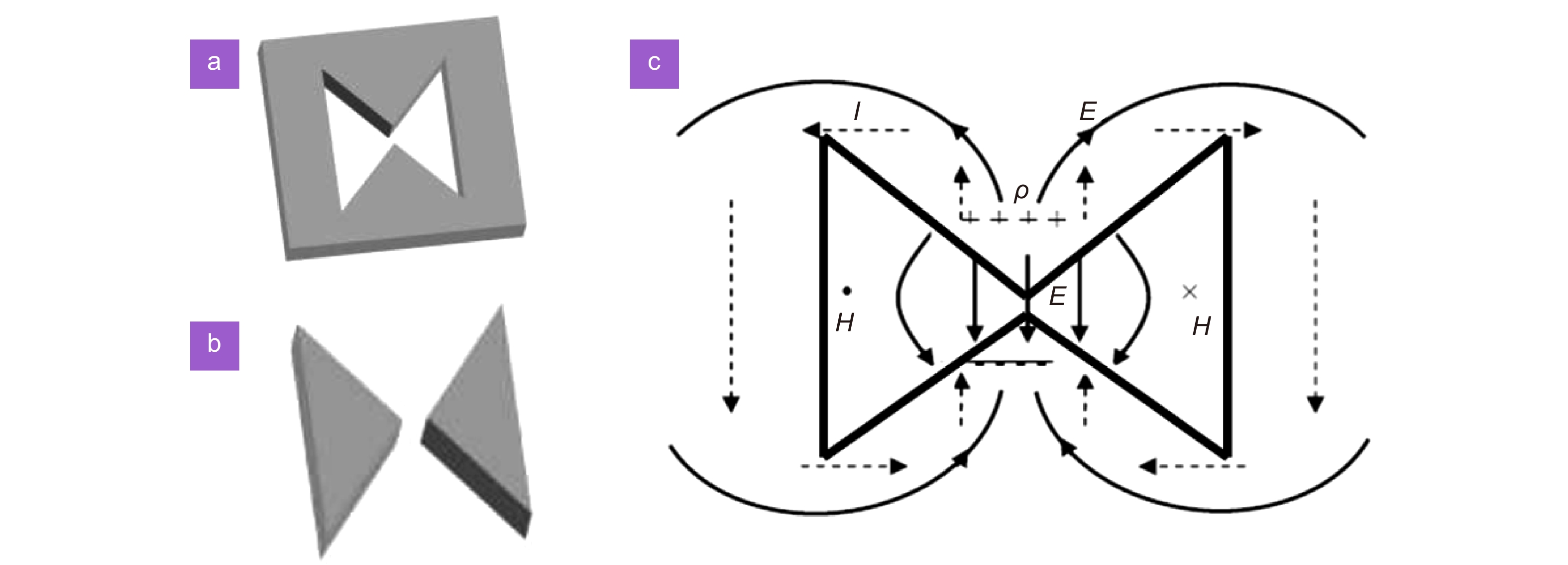
It has been a long time for researchers to explore methods to overcome the diffraction limit. Although light can be squeezed through a sub-wavelength hole1 leading to lateral resolution on the order of the hole size, its transmission is very limited based on Bethe’s law2. However, it has been noticed that bowtie antennas (Fig. 1(a)) enable simultaneous high resolution and enhanced transmission3, which is suitable for near-field imaging techniques such as scanning near-field optical microscopy (SNOM) and near field lithography. This phenomenon can be simply explained as follows. The two arms of the bowtie antenna have large surface areas to efficiently collect the incident radiation. Incident light polarized along the gap of the bowtie antenna generates surface currents to carry surface charge to the sharp tips (Fig. 1(c)). The opposite oscillating surface charges at the tips behave like an oscillating electric dipole which radiates light through the aperture. Therefore, light with proper polarization can pass through the bowtie antenna without experiencing much intensity decay. The transmitted light is confined underneath the nanoscale gap region offering an optical resolution far beyond the diffraction limit.
![Figure 1. Bowtie apertured (a) and gaped (b) antennas. (c) Induced surface charges and electric dipole when incident electric field polarizes along the tips. Figure reproduced with permission from: (a-b) ref.4, Copyright 2006 American Chemical Society.]()
Bowtie apertured (a) and gaped (b) antennas. (c) Induced surface charges and electric dipole when incident electric field polarizes along the tips. Figure reproduced with permission from: (a-b) ref.4, Copyright 2006 American Chemical Society.
In a more general way, bowtie antennas (hereafter, bowties) acting as optical antennas, receive and emit radiation as they do in the microwave regime5, 6. It means that bowties, regardless of whether it is apertured (Fig. 1(a)) or gaped (Fig. 1(b)), can convert an external electromagnetic field into a confined energy7, 8, and vice versa. Field confinement and enhancement presented in the gap region, thus can be utilized to achieve a variety of optical applications.
Since the early 2000s, bowtie structures have been used as electrodes in molecular engineering9 and applied in molecular junctions to investigate electroluminescence10, and high-conductivity11, 12. Thanks to the development of nanofabrication, bowties in nanometer scale dimensions13-15 brought about widespread optical applications. In 2006, sub-diffraction nanoscale lithography with bowties4, 16 have been demonstrated. Nanolaser based on bowties array was achieved by exciting dye molecules centered in the gap, in 201217. In 2018, enhanced absorption via bowtie arrays in 2D black phosphorus was achieved based on the high transmission of the antenna and a perfect polarization selection ratio is observed18. Recently, nanoscale bowties were reported to be excited by not only external light, but also electricity19, showing its advantages in high intensity and ultrafast optical response. As we will show, the last decades have witnessed the booming development of bowties under the optical or electrical excitation.
This paper aims to review applications of optically and electrically driven nanoscale bowties. Since rapid advances have been made in this area, it is difficult to cover all the related references in this review. Nonetheless, we hope the present review arouse interest among the researchers in this subject.
Optically driven nanoscale bowties
Due to the high enhancement and confinement of bowties, strong electric field localizations20-22 (hot spots) are presented in the gap. These properties promise bowties broad applications ranging from light transmitting, frequency doubling/tripling, focusing, and generation to detection. In this section, we present an overview of the applications of optically excited bowties.
Nanoimaging and nanotrapping
As mentioned before, bowties exhibit highly enhanced fields under the illumination of light. The consequently enhanced light transmission guarantees a set of nanotechnologies such as nanoimaging and trapping.
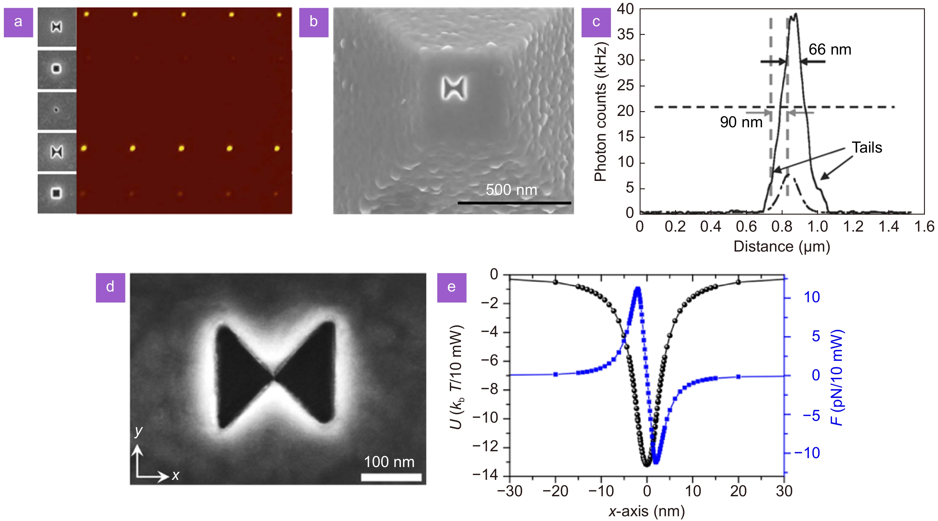
Near-field imaging techniques, e.g., SNOM, utilizes evanescent waves to generate sub-diffraction-limit resolution. As the evanescent components decay exponentially, SNOM uses a tapered fiber23 as a probe and needs to work close to the sample surface. Even in this situation, the light coupling efficiency is severely limited because of the poor transmission of the fiber tip. Therefore subwavelength apertures are usually constructed on the tip apex to boost the light collection. Bowtie apetures3, 24 are favored over other apertures owing to its giant light field enhancement13. Wang et al.3 fabricated metallic bowtie and square apertures on the quartz wafer, and compared their far-field transmission (Fig. 2(a)). Results indicated that the transmission was enhanced exceeding one order of magnitude from bowtie apertures than the squared ones with the same opening areas. Bowtie apertures were then milled on the SNOM probe (Fig. 2(b)), showing a seven times higher near-field measurement counts than the regular aperture probe (Fig. 2(c)).
![Figure 2. Near-field imaging and trapping using (apertured) bowties. (a) Transmission through the subwavelength apertures. Bowtie apertures show much enhanced transmission. Left: different apertures. Right: far-field transmission measurements. (b) Bowtie apertures fabricated on the SNOM probe. (c) Line profiles of SNOM images using bowtie (solid line) and square (dashed line) aperture probes. (d) 5-nm-gap bowtie apertures. (e) Optical potentials U and the corresponding optical forces F along the x-axis. Figure reproduced with permission from: (a–c) ref.3, Copyright 2007 AIP Publishing; (d–e) ref.27, Copyright 2018 the author(s), under a Creative Commons Attribution 4.0 International License.]()
Near-field imaging and trapping using (apertured) bowties. (a) Transmission through the subwavelength apertures. Bowtie apertures show much enhanced transmission. Left: different apertures. Right: far-field transmission measurements. (b) Bowtie apertures fabricated on the SNOM probe. (c) Line profiles of SNOM images using bowtie (solid line) and square (dashed line) aperture probes. (d) 5-nm-gap bowtie apertures. (e) Optical potentials U and the corresponding optical forces F along the x-axis. Figure reproduced with permission from: (a–c) ref.3, Copyright 2007 AIP Publishing; (d–e) ref.27, Copyright 2018 the author(s), under a Creative Commons Attribution 4.0 International License.
Strong energy confinement with a high optical gradient provided by bowties also promises applications in optical trapping25-27. Using a bowtie plasmonic aperture that was patterned on a tapered metal-coated fiber25, 50 nm polystyrene beads were successfully captured, demonstrating the feasibility of nanoparticle trapping. Notably, 4-nm quantum dot was experimentally reported to be trapped in a deep potential well (Fig. 2(e)) using the three-dimensional tapered 5-nm-gap bowtie aperture antenna (Fig. 2(d)).
Nonlinear response
Typically optical antennas work in the linear regime for weak excitation fields. In other words, the nonlinearity is negligible in most cases. The nonlinear conversion efficiency, however, can be resonantly enhanced by localized surface plasmons (LSPs)28 when appropriate size and shape of the nanoantenna are introduced. As a consequence, new interesting phenomena arise, such as frequency conversion, switching, and modulation29.
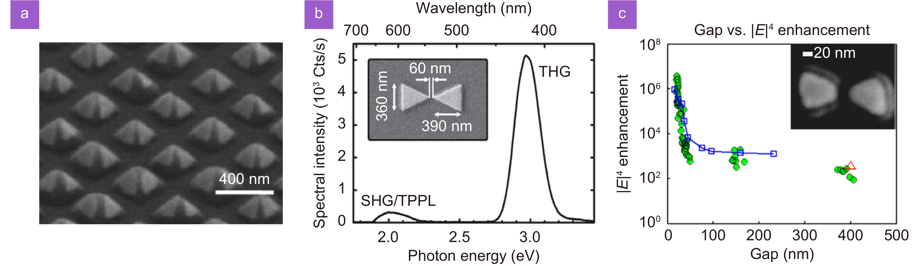
Bowties exhibit power enhancement factors larger than 40 dB30, which is beneficial to second or even higher order harmonics generation31. As shown in Fig. 3(a), large arrays of antennas are often used to boost nonlinear conversion efficiency32-34. Nevertheless, Hanke et al.35 observed that third harmonic (visible light) was emitted by using individual bowtie antenna excited resonantly with few-cycle femtosecond laser (~0.6 MW/cm2) in the near infrared. Though the second-order harmonic generation is partially constrained by the symmetry condition, it was also observed in the emission spectra with a small peak (Fig. 3(b)). It has been reported30 that bowties are even capable of lowering the pulsed femtosecond laser intensities (from 1013 MW/cm2 to 1011 MW/cm2 level) that are required to produce coherent extreme-ultraviolet (EUV) light through the nonlinear conversion process. High harmonics up to 17th were observed.
![Figure 3. Nonlinear response in bowties. (a) Three-dimensional (3D) gold bowties array. (b) Nonlinear emission spectrum from a single bowtie (inset). (c) Spectrum of generated high harmonics from 2D bowties array (inset). (d) Experimental (TPPL, circles) and theoretical (field enhancement, squares) results versus bowtie gap size. Inset shows a bowtie with a 22 nm gap. Figure reproduced with permission from: (a) ref.32, American Chemical Society; (b) ref.35, under a Creative Commons Attribution 3.0 License; (c) ref.15, American Physical Society.]()
Nonlinear response in bowties. (a) Three-dimensional (3D) gold bowties array. (b) Nonlinear emission spectrum from a single bowtie (inset). (c) Spectrum of generated high harmonics from 2D bowties array (inset). (d) Experimental (TPPL, circles) and theoretical (field enhancement, squares) results versus bowtie gap size. Inset shows a bowtie with a 22 nm gap. Figure reproduced with permission from: (a) ref.32, American Chemical Society; (b) ref.35, under a Creative Commons Attribution 3.0 License; (c) ref.15, American Physical Society.
Two-photon photoluminescence (TPPL) can also occur because of high local fields at LSP resonance and shows E4local dependence on the local E fields15 (Fig. 3(c)).
Nanolithography
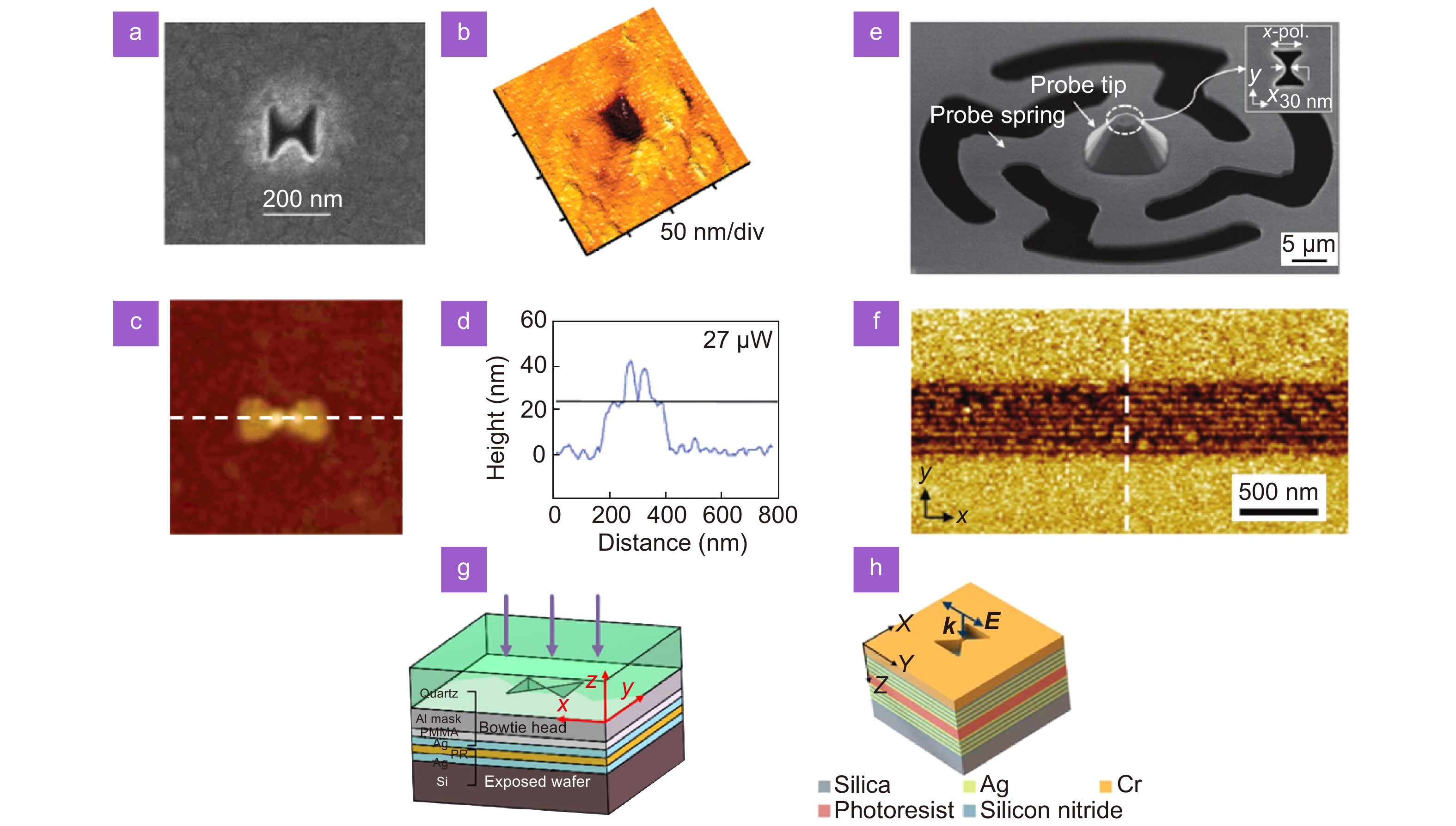
The development of modern information technologies makes a request of advanced nano-manufacturing tools. As we will see, great success has been achieved in nanolithography via bowties in the last decades. Bowties are capable of focusing the incident ultra-violet (UV) light into a small spot, showing remarkable advantages over traditional optical lithography, e.g., deep UV and extremely UV lithography, for its low cost and competitive resolution. In 2006 Wang et al.4 fabricated apertured bowties by focused ion beam (FIB) on a 150 nm thick aluminum film (Fig. 4(a)). Under the illumination of 355 nm light, 40×50 nm lithography resolution was experimentally reported, as shown in Fig. 4(b). Higher resolution becomes more noticeable by fabricating an ultra-small gap between the antenna tips with the back-side milling method36. Another nice experiment was conducted by Sundaramurthy et al.16 in the same year. They demonstrated that by utilizing optically resonant metallic bowties, the production of polymer resist nanostructures <30 nm in diameter was achieved at a longer wavelength of 800 nm via the two-photon polymerization (TPP) effect (Fig. 4(c) and 4(d). Researchers37 from Yonsei University has shown that by using a contact probe made of bowtie aperture antennas (Fig. 4(e)) illuminated by a 405 nm wavelength laser light, high-density line array patterns were recorded with a half pitch up to 22 nm (Fig. 4(f)). Further, the line edge roughness was decreased down to be ~ 17 nm by optimizing the developing process. This work implies bowties-based nanolithography has a great potential for practical applications.
![Figure 4. Nanolithography using bowties. (a) Bowtie apertures with a 30 nm gap. (b) AFM image of 40 nm × 50 nm lithography hole. (c–d) AFM image (c) and cross section (d) along the nanoantenna axis of bowties exposed at 25 μW laser power. Feature size of ~30 nm for each of the resist pillars was measured. (e) SEM image of the fabricated circular contact probe. (f) AFM image of a 22-nm half pitch resolution line array pattern. (g–h) Bowtie nanolithography combined with metal-insulator-metal (g) and hyperbolic metamaterials (h). Figure reproduced with permission from: (a, b) ref.4, Copyright 2016 American Chemical Society; (c, d) ref.16, American Chemical Society; (e, f) ref.37, Copyright 2012 John Wiley and Sons; (g) ref.38, Copyright 2019 Optical Society of America; (h) ref.41, IOP Publishing.]()
Nanolithography using bowties. (a) Bowtie apertures with a 30 nm gap. (b) AFM image of 40 nm × 50 nm lithography hole. (c–d) AFM image (c) and cross section (d) along the nanoantenna axis of bowties exposed at 25 μW laser power. Feature size of ~30 nm for each of the resist pillars was measured. (e) SEM image of the fabricated circular contact probe. (f) AFM image of a 22-nm half pitch resolution line array pattern. (g–h) Bowtie nanolithography combined with metal-insulator-metal (g) and hyperbolic metamaterials (h). Figure reproduced with permission from: (a, b) ref.4, Copyright 2016 American Chemical Society; (c, d) ref.16, American Chemical Society; (e, f) ref.37, Copyright 2012 John Wiley and Sons; (g) ref.38, Copyright 2019 Optical Society of America; (h) ref.41, IOP Publishing.
While sub-diffraction resolution (<20 nm)36 can be achieved by using bowties, nearly all the aforementioned results suffer from a small depth of focus (DOF: <10 nm), which poses challenges for industrial production. Such a problem is alleviated by combining bowtie antennas with metamaterials, such as silver superlens/reflectors38-40 (Fig. 4(g), DOF: ~30 nm) and hyperbolic metamaterials41 (Fig. 4(h), DOF: ~100 nm). However, the DOF has to be larger than 100 nm to realize convenient and reliable pattern transferring. This has to be addressed before taking bowtie nanolithography a step closer to widespread applications.
Nanosources
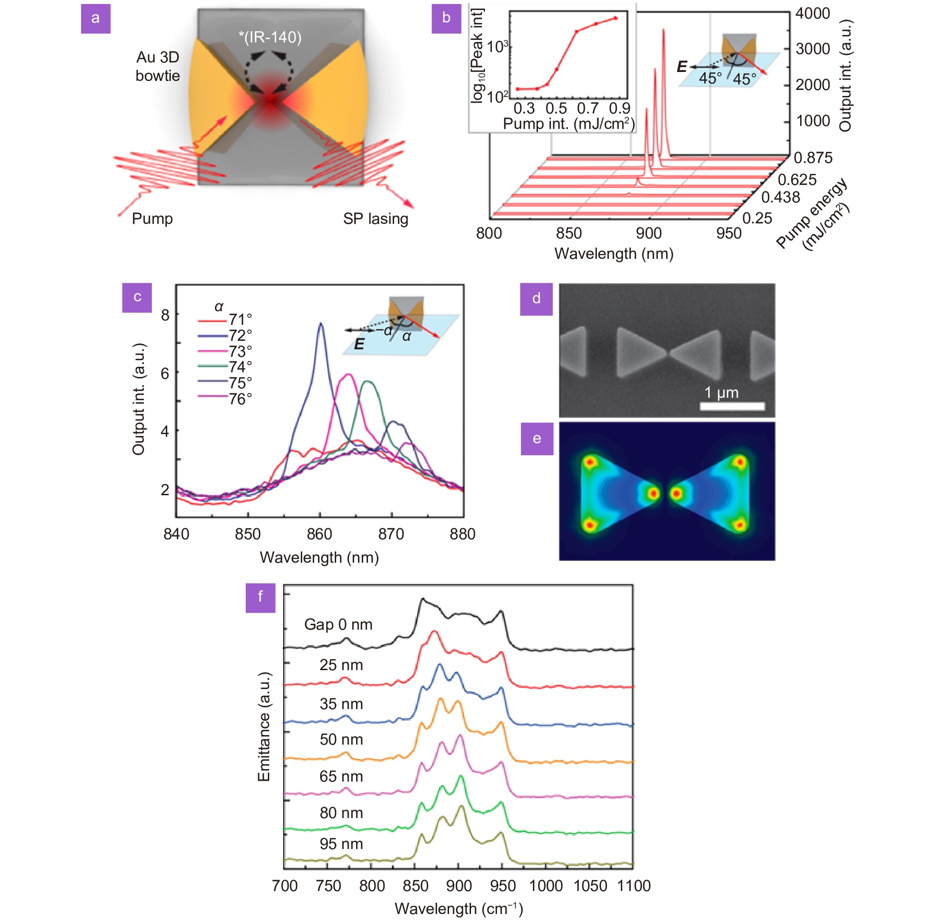
Miniaturized photon sources are essential elements for all-optical circuits and nanoscale biosensors. One way of achieving lasing from nanoscale resonators is to utilize LSPs excited in metal nano-particles. A bowtie-shaped metallic resonator are well suited for this purpose as it can provide high Purcell factor thanks to the high confinement, therefore, the ultra-small effective mode volume42. In addition, the threshold condition for lasing can be satisfied at room temperature near LSP resonance wavelengths. Shown in Fig. 5(a), Jae Yong Suh et al.17 demonstrated that three-dimensional (3D) nano-bowties array coupled with a gain medium (IR-140 dye in polyurethane) can generate coherent and directional light emission (Fig. 5(b) and 5(c)). With a mode volume smaller than 0.001(λ/2n)3 (λ, the wavelength and n, the effective refractive index), room temperature optically pumped lasing at 873 nm with a threshold pump pulse fluence of 0.4 mJ/cm2 was observed.
![Figure 5. Bowtie based nanosources. (a) Schematic of 3D bowtie plasmonic lasers. (b) Evolution of lasing spectra from 3D Au bowties under pump polarization parallel to the tip axis. Inset shows emission intensity versus pump pulse energy density plotted on a semilogarithmic scale. (c) Directional SP out-coupling emission. (d) Bowties with a small gap. (e) Simulated near-field patterns of one of resonant modes in bowties. (f) Thermal emission spectrum under different bowtie gap sizes. Figure reproduced with permission from: (a–c) ref.17, Copyright 2012 American Chemical Society; (d–f) ref.44, Copyright 2017 the author(s), under the ACS AuthorChoice via CC-BY-NC-ND Usage Agreement.]()
Bowtie based nanosources. (a) Schematic of 3D bowtie plasmonic lasers. (b) Evolution of lasing spectra from 3D Au bowties under pump polarization parallel to the tip axis. Inset shows emission intensity versus pump pulse energy density plotted on a semilogarithmic scale. (c) Directional SP out-coupling emission. (d) Bowties with a small gap. (e) Simulated near-field patterns of one of resonant modes in bowties. (f) Thermal emission spectrum under different bowtie gap sizes. Figure reproduced with permission from: (a–c) ref.17, Copyright 2012 American Chemical Society; (d–f) ref.44, Copyright 2017 the author(s), under the ACS AuthorChoice via CC-BY-NC-ND Usage Agreement.
Bowties also show great potential for high-contrast selection of single nanoemitters43. Kinkhabwala et al.43 observed enhancements of a single molecule’s fluorescence up to a factor of 1340 by using fluorescent molecules coated bowties. They attributed this to the result of greatly enhanced absorption and an increased radiative emission rate due to the presence of bowties.
Moving towards the infrared band, silicon carbide bowties (Fig. 5(d)) can serve as a thermal emitter with a narrowband (10 cm−1) spectrum44 (Fig. 5(f)), which is suitable for novel applications such as non-dispersive infrared sensing and molecular spectroscopy. The thermal emission spectrum show a clear dependence on the bowtie gap size, indicating that a tunable thermal emitter is achievable. Numerical simulations (Fig. 5(e)) and near-field optical characterization shade light on the physical nature of the resonances in the thermal emission spectra.
Photodetectors
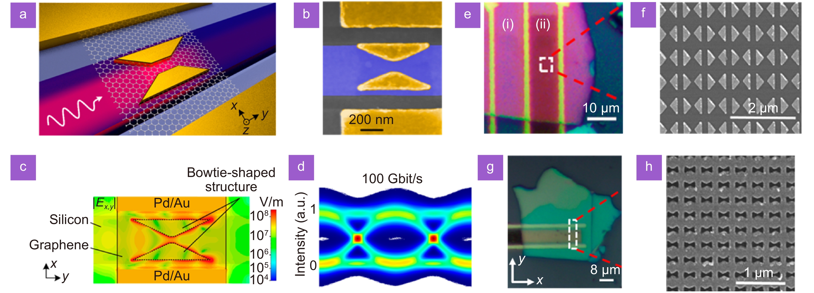
The strong plasmonic enhancement between the bowtie tips results in an enhanced in-plane electric fields interaction with two-dimensional (2D) materials, leading to an efficiently absorbed external light. Consequently, bowties have been utilized to enhance the responsivity of photodetectors. For example, Ma et al.45 reported that a bowtie-enhanced graphene waveguide photodetector possesses a high external responsivity of 0.5 A/W and a fast frequency response up to at least 110 GHz (Fig. 6(a–c)). As a validation of optical communication, 100 Gbit/s data reception of two-level OOK and four-level PAM-4 intensity encoded signals was successfully demonstrated at C-band (Fig. 6(d)). Venuthurumilli et al.18 also demonstrated a near infrared photodetector using black phosphorus embellished by bowties, as shown in Fig. 6(e) and 6(g). High photocurrent (an enhancement of 70% in comparison to the device without bowties, Fig. 6(f)) or polarization sensitivity (8.7, Fig. 6(h)) can be achieved with proper bowtie designs and orientations.
![Figure 6. 2D materials photodetectors based on bowties. (a) Schematic and (b) SEM image of the plasmonically enhanced graphene photodetector. (c) The magnitude of in-plane electric fields. Strong plasmonic field enhancements in the gap were observed. (d) Eye diagram of 100 Gbit/s OOK optical signals. (e) Optical and (f) SEM image of bowtie gap antennas for high responsivity detectors. (g) Optical and (h) SEM image of bowtie aperture antennas for high polarization. Figure reproduced with permission from: (a–d) ref.45, Copyright 2019 The Author(s), under the ACS AuthorChoice Usage Agreement; (e–h) ref.18, Copyright 2018 American Chemical Society.]()
2D materials photodetectors based on bowties. (a) Schematic and (b) SEM image of the plasmonically enhanced graphene photodetector. (c) The magnitude of in-plane electric fields. Strong plasmonic field enhancements in the gap were observed. (d) Eye diagram of 100 Gbit/s OOK optical signals. (e) Optical and (f) SEM image of bowtie gap antennas for high responsivity detectors. (g) Optical and (h) SEM image of bowtie aperture antennas for high polarization. Figure reproduced with permission from: (a–d) ref.45, Copyright 2019 The Author(s), under the ACS AuthorChoice Usage Agreement; (e–h) ref.18, Copyright 2018 American Chemical Society.
Electrically driven nanoscale bowties
Nanoantennas can be excited by not only the external light, but also the bias voltages. They function as an emerging optical nano-source46-49 via the inelastic electron tunneling (IET) process. Related researches can date back to 1976 in biased metal-insulator-metal junctions50, and lately, in scanning tunneling microscope (STM) systems51-53. Electrically driven antennas bridge electrical and optical circuits at the nanoscale and constitute a vibrant sub-field of nano-photonics.
We also notice that bowtie-shaped metallic structures are widely used in molecule engineering as electrical leads, to exploit charge transport at the level of single molecules54. Strictly speaking, however, these devices can hardly be regarded as ‘antennas’ due to the lack of related functions. Therefore in this section, we will devote special attention to light emission from electrically excited bowtie antennas, including the principles, fabrication, characterizations and future directions.
Underlying mechanisms
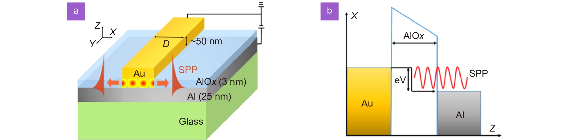
A tunnel junction can be made of a thin insulating layer (usually the air or, here, oxide) sandwiched between the two conducting materials (e.g., here, Al and Au), as illustrated in Fig. 7(a). When voltages are applied, electrons could tunnel through the barrier inelastically and give rise to an energy transfer in the form of (localized or propagated) surface plasmons (Fig. 7(b)). Light can be emitted by the radiative decay or scattering of surface plasmons55. Since the tunneling process happens at a time scale of femtoseconds56, 57, it enables electrically driven antennas to be operated as an ultrafast optical source.
![Figure 7. Surface plasmons mediated via the IET process. (a) Schematic of the Al-AlOx-Au tunnel junction. (b) Energy level diagram of the IET process. (c) Bias dependent emission spectra. Emitted photons with cut-off frequencies can be seen. Figure reproduced with permission from ref.49, under a Creative Commons Attribution 4.0 International License.]()
Surface plasmons mediated via the IET process. (a) Schematic of the Al-AlOx-Au tunnel junction. (b) Energy level diagram of the IET process. (c) Bias dependent emission spectra. Emitted photons with cut-off frequencies can be seen. Figure reproduced with permission from ref.49, under a Creative Commons Attribution 4.0 International License.
A typical signature of IET is that the cut-off frequency ν in electroluminescence spectrum is related to the applied bias voltage Vbias (Fig. 8(c)), also known as the quantum limit hν⩽ in which h the Planck’s constant and e the electron charge. Interestingly, an alternative mechanism that might explain the light emission from tunnel junctions is resulted from hot-electron decay58, where the energies of emitted photons are beyond the quantum limit. Our focus is concentrated on the IET process. IET can be theoretically described as an energy-loss model, current fluctuations model and spontaneous emission model. We refer the interested readers to the review59 for more mathematic details. Here, we briefly give a physical picture behind light emission from electrically driven antennas, as follows.
The (detectable) electron-to-photon conversion efficiency, or, the external quantum efficiency (EQE) driven by IET can be described as
{\rm{EQE = }}\eta _0^{{\rm{IET}}}\frac{{{P_{{\rm{total}}}}}}{{{P_0}}}\frac{{{P_{{\rm{rad}}}}}}{{{P_{{\rm{total}}}}}}\;, where \eta _0^{{\rm{IET}}} is the source efficiency of IET in vacuum (in the order of 10–6 level at visible frequencies with a modest dependence on the details of the barriers59), {P_0} is the power emitted by a dipole in free space, {P_{{\rm{total}}}} is the total power dissipated (not directly to photon emission but often in the form of other types of optical modes, such as LSP modes) by a dipole in an arbitrary environment and {P_{{\rm{rad}}}} is the radiated power. The key is that, the ratio of {P_0} and {P_{{\rm{total}}}} is deeply connected to the quantity, the partial local density of the optical states (LDOS) {\rho _{\rm{p}}}, that is59
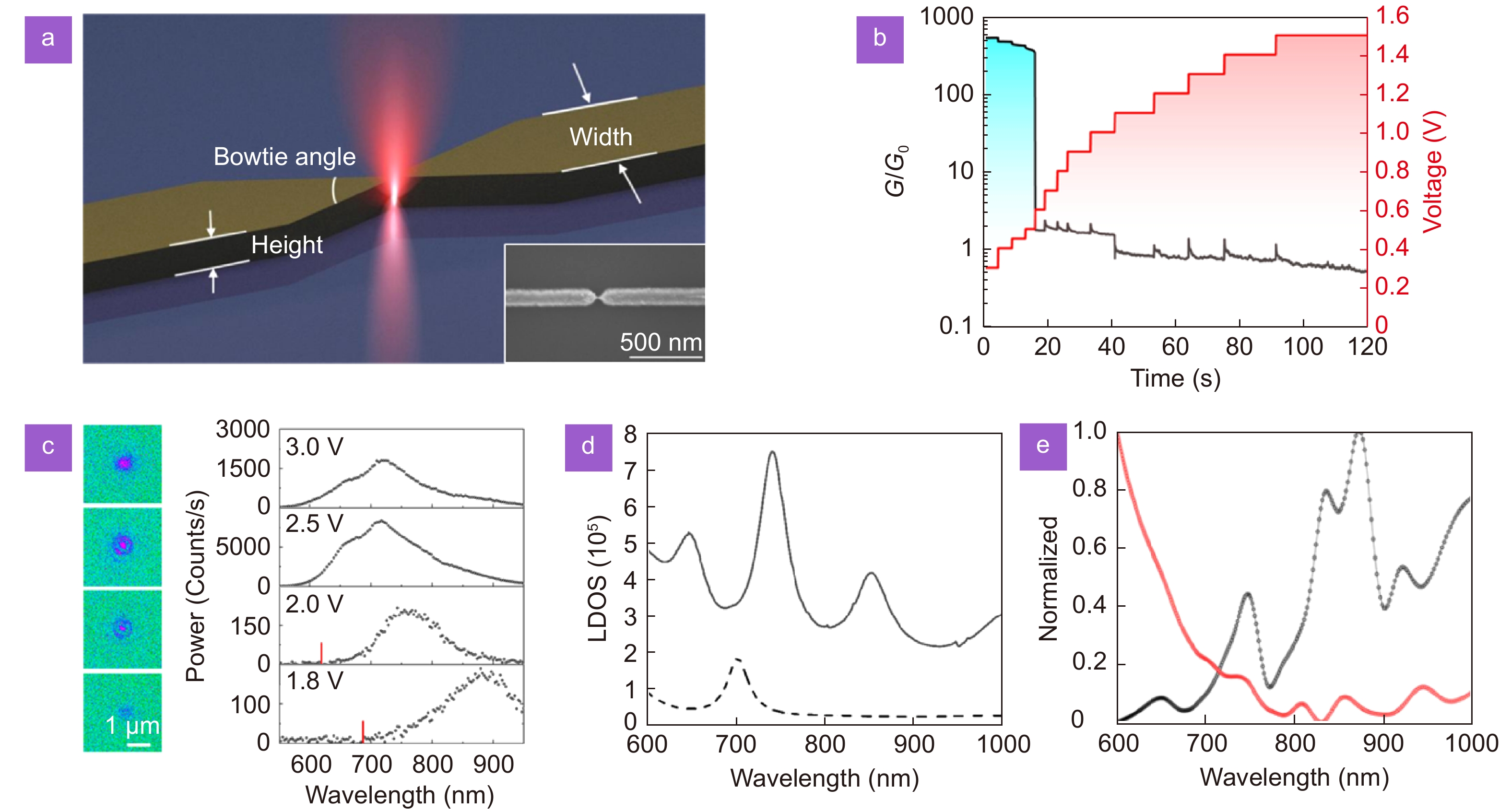
\frac{{P}_{\rm{total}}}{{P}_{0}}=\frac{{\rho }_{\rm{p}}}{{\rho }_{0}}\;, where {\rho _0} is the vacuum LDOS. The radiation efficiency {\eta _{{\rm{rad}}}} is defined as {P_{{\rm{rad}}}}/{P_{{\rm{total}}}}. Both the LDOS and radiation efficiency (Fig. 8(d) and 8(e)) are profoundly influenced by the geometries of bowties (say, for example, the bowtie width, height and angle shown in Fig. 8(a)). This demonstrates the practicality of tunable nano-sources based on bowtie junctions. Although the LDOS and {\eta _{{\rm{rad}}}} cannot be analytically expressed except a few kinds of geometries, Eq. (2) points out a viable way of estimating EQE by numerical simulations using the Green’s function60.
![Figure 8. Light emission from bowtie antenna based tunnel junctions. (a) Lateral tunnel junctions made by bowtie gap-antennas. Inset shows that the bowtie antennas are connected before the electro-migration process. (b) Time evolution of normalized conductance (G/G0). (c) Light emission spectra. Left column: images captured under different biases. Right column: spectral evolution under different bias. (d) Enhanced LDOS in the order of 105. Solid line: bowties case. Dashed lines: nanowire case. (e) Wavelength dependent normalized LDOS (red) and radiation efficiency (black). They both contribute to the ultimate emission spectrum. Figure reproduced with permission from: (a–d) ref.19, Copyright 2019 American Chemical Society; (e) ref.64, Copyright 2020 Optical Society of America.]()
Light emission from bowtie antenna based tunnel junctions. (a) Lateral tunnel junctions made by bowtie gap-antennas. Inset shows that the bowtie antennas are connected before the electro-migration process. (b) Time evolution of normalized conductance (G/G0). (c) Light emission spectra. Left column: images captured under different biases. Right column: spectral evolution under different bias. (d) Enhanced LDOS in the order of 105. Solid line: bowties case. Dashed lines: nanowire case. (e) Wavelength dependent normalized LDOS (red) and radiation efficiency (black). They both contribute to the ultimate emission spectrum. Figure reproduced with permission from: (a–d) ref.19, Copyright 2019 American Chemical Society; (e) ref.64, Copyright 2020 Optical Society of America.
Fabrication of bowtie antenna based tunnel junctions
Tunnel junctions can be classified into two categories, namely, the vertical (for example, shown in Fig. 7(a)) and lateral junctions (Fig. 8(a)) , in terms of their orientations relative to the substrate. As for the vertical junctions, they are formed due to the nature of oxidation. When it comes to the lateral counterpart, while the ultra-small (sub 1 nm) gap is hard to fabricate using currently available nanopatterning methods61, electro-migration62, 63 is a good choice to generate bowtie gap-antenna tunnel junctions. This process19, 64 starts with the patterning of weakly-bridged (the smallest linewidth is 10 nm) bowties by electron beam lithography, followed by supplying a gradually-increasing bias voltages till the conductance G of the antennas drops well below the quantum conductance65 {G_0} = 2{{\rm{e}}^2}/h (shown in Fig. 8(b)). It is at this stage that a tiny gap appears. Our group has demonstrated a 0.6 nm gap bowtie antenna19 obtained by a well-controlled electro-migration process.
Characterizations
Thanks to the well-designed bowtie gap-antenna tunnel junctions, we have achieved a broadband optical nano-source driven by IET (see Fig. 8(c)) with peak emission power of 1.4 nW19, which is two orders of magnitude higher than previous results (see Table 1). The EQE is then calculated to be (1.1 ± 0.2) × 10–4. It is not hard to understand either from the point view of enhanced LDOS (see Fig. 8(d)), or enhanced Purcell factors66 due to the small mode volume in bowties. Further, bowtie-shaped structures also function as ‘antennas’, providing a high radiation efficiency (of course, at specific wavelengths). Accordingly, the emission spectrum can be tuned by engineering LDOS and radiation efficiency (Fig. 8(e)), as explained in Underlying Mechanisms. Wang et al. recently have used an approximate model64 to analytically calculate the resonant peaks in the emission spectra of electrically driven bowties, showing a good agreement with the experimental results.
Comparison on the performance of tunnel junctions
References Width of the tunnel gap Tunnel current Type of the tunnel junction Output power EQE Measuring tool EMCCD: electron-multiplying charge-coupled device sCMOS: scientific complementary metal–oxide–semiconductor ref.46 1.3 nm ~2 nA @ 1.5 V Au-air-Au / 3×10⁻⁴ EMCCD ref.47 2.0 nm ~10 nA Al-AlOx–Au / / EMCCD ref.48 1.5 nm ~25 nA @ 2.5 V Ag-PVP-Ag 30 pW 2×10⁻³ EMCCD ref.69 1.1 nm ~10 nA @ 1.5 V Au-air-Au / ~1×10⁻⁵ EMCCD ref.72 30 nm ~100 nA @15 V Au-air-Au / / EMCCD ref.19 0.6 nm ~5 μA @ 2.5 V Au-air-Au 1.4 nW ~1.1×10⁻⁴ sCMOS Future directions
Higher efficiencies48 are continually pursued by researchers. While EQE roughly shows a dependence on the width d of tunnel gap (d–1)59, however, d cannot be unlimited shortened because quantum mechanics dominates then. The operating speed and footprint may be priority depending on applications. In recent years, two-dimensional materials integrated tunnel devices67, 68 attract much attention and remain to be further explored. Directional control of electrically excited sources69-71 via IET is also of particular interest by using properly designed antenna architectures.
Summary
Owing to the field confinement and enhancement, nanoscale bowties can be a good fit for a variety of applications such as near-field imaging, nanotrapping, nanolithography, nano-sources and photodetectors, etc. This review presents the applications of nanoscale bowties excited by photons and electrons. Bowties can be used for bridging electronic and photonic components on a same chip, thus possessing great potential in high-density optical storage and on-chip wireless communication. Nanoscale bowties may meet great challenges but could also lead photonic chip researches to a new step in the future.
Acknowledgements
This work is supported by National Key Research and Development Program of China (2018YFB2200900), the Key R&D Program of Anhui (Grant No. 202004A05020077) and National Natural Science Foundation of China (61775206). The nanofabrication was carried out at the USTC Center for Micro and Nanoscale Research and Fabrication. We also thank Prof. Xianfan Xu of Purdue University for his warm-hearted discussion.
Competing interests
The authors declare no competing financial interests.
-
References
[1] Synge EH. XXXVIII. A suggested method for extending microscopic resolution into the ultra-microscopic region. London, Edinburgh, Dublin Philos Mag J Sci 6, 356–362 (1928).
DOI: 10.1080/14786440808564615[2] Bethe HA. Theory of diffraction by small holes. Phys Rev 66, 163–182 (1944).
DOI: 10.1103/PhysRev.66.163[3] Wang L, Xu XF. High transmission nanoscale bowtie-shaped aperture probe for near-field optical imaging. Appl Phys Lett 90, 261105 (2007).
DOI: 10.1063/1.2752542[4] Wang L, Uppuluri SM, Jin EX, Xu XF. Nanolithography using high transmission nanoscale bowtie apertures. Nano Lett 6, 361–364 (2006).
DOI: 10.1021/nl052371p[5] Balanis CA. Antenna Theory: Analysis and Design (Harper & Row, New York, 1982).
[6] Grober RD, Schoelkopf RJ, Prober DE. Optical antenna: towards a unity efficiency near-field optical probe. Appl Phys Lett 70, 1354–1356 (1997).
DOI: 10.1063/1.118577View full references list -
Cited by
Periodical cited type(10)
1. Shen, Z., Lv, B., Yi, Z. et al. Dual-frequency polarization-insensitive and wide-angle metasurface for electromagnetic energy harvesting. Photonics and Nanostructures - Fundamentals and Applications, 2025. DOI:10.1016/j.photonics.2024.101328 2. Li, Y., Luo, Y., Lin, X. et al. Metal-insulator-metal (MIM) star-disc nanoantenna for molecular sensing by surface-enhanced infrared absorption (SEIRA) spectroscopy. Surfaces and Interfaces, 2025. DOI:10.1016/j.surfin.2025.105758 3. Babicheva, V.E., Rumi, M. Chalcophosphate metasurfaces with multipolar resonances and electro-optic tuning. RSC Advances, 2024, 14(46): 33906-33918. DOI:10.1039/d4ra05149a 4. Du, J., Bao, W., Zhang, R. et al. Manipulation of unidirectional side scattering of light in transition metal dichalcogenide nanoresonators. Physical Review B, 2024, 109(11): 115426. DOI:10.1103/PhysRevB.109.115426 5. Zhu, H., Xu, Y., Zhang, T. et al. Reconfigurable Generalized Joined Coupler Matrices for Independent Control of Multiple Steerable Beams. IEEE Transactions on Antennas and Propagation, 2024. DOI:10.1109/TAP.2024.3503915 6. V. Grayli, S., Kamal, S., Leach, G.W. High performance, single crystal gold bowtie nanoantennas fabricated via epitaxial electroless deposition. Scientific Reports, 2023, 13(1): 12745. DOI:10.1038/s41598-023-38154-1 7. Jiang, Z., He, W., Chen, J. et al. Plasmonic direct-writing lithography via high numerical aperture objectives. Optics Letters, 2023, 48(15): 4153-4156. DOI:10.1364/OL.496697 8. Song, J., Liu, B., Shan, X. et al. Multi-functional dual-path self-aligned polarization interference lithography. Optics Express, 2023, 31(11): 17629-17644. DOI:10.1364/OE.489049 9. Xie, P., Ding, Q., Liang, Z. et al. Cavity-assisted boosting of self-hybridization between excitons and photonic bound states in the continuum in multilayers of transition metal dichalcogenides. Physical Review B, 2023, 107(7): 075415. DOI:10.1103/PhysRevB.107.075415 10. Xie, P., Deng, Y., Zeng, L. et al. Tunable interactions of quasibound states in the continuum with cavity mode in a metasurface-microcavity hybrid. Physical Review B, 2022, 106(16): 165408. DOI:10.1103/PhysRevB.106.165408 Other cited types(0)
-
Author Information
-
Copyright
Open Access. © The Author(s). This article is licensed under a Creative Commons Attribution 4.0 International License. To view a copy of this license, visit http://creativecommons.org/licenses/by/4.0/. -
About this Article
Cite this Article
Zhongjun Jiang, Yingjian Liu, Liang Wang. Applications of optically and electrically driven nanoscale bowtie antennas. Opto-Electronic Science 1, 210004 (2022). DOI: 10.29026/oes.2022.210004Download CitationArticle History
- Received Date June 07, 2021
- Accepted Date November 03, 2021
- Available Online April 19, 2022
- Published Date April 19, 2022
Article Metrics
Article Views(8257) PDF Downloads(895)
 OE Journals Group

Reports the physical mechanisms and fundamental science of optics, photonics and optoelectronics
Open Access