E-mail Alert
 RSS
RSS-
Abstract
Metasurfaces, two-dimensional equivalents of metamaterials, are engineered surfaces consisting of deep subwavelength features that have full control of the electromagnetic waves. Metasurfaces are not only being applied to the current devices throughout the electromagnetic spectrum from microwave to optics but also inspiring many new thrilling applications such as programmable on-demand optics and photonics in future. In order to overcome the limits imposed by passive metasurfaces, extensive researches have been put on utilizing different materials and mechanisms to design active metasurfaces. In this paper, we review the recent progress in tunable and reconfigurable metasurfaces and metadevices through the different active materials deployed together with the different control mechanisms including electrical, thermal, optical, mechanical, and magnetic, and provide the perspective for their future development for applications.
Keywords
-
Introduction
The importance of active, tunable, or reconfigurable devices in modern electromagnetic and photonic systems is undebatable. It is highly desirable to create such metasurfaces capable of dynamic manipulations of the incident wave. For example, tunable frequency selectively or perfectly absorbing metasurfaces allows accurate resonance tuning to perfectly match the operational condition or switching of operational frequency in signal modulation. A tunable metalens made from active wave-front shaping metasurface allows fine tuning of focal length which is very desirable in the imaging process.
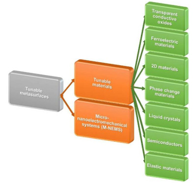
Each type of these materials has different properties and tuning mechanisms. For example, indium tin oxide (ITO) can be stimulated electrically85 and optically59, and liquid crystals can be tuned electrically108, optically101, thermally109, and magnetically67. Moreover, the electrical tuning of the transparent conductive oxides is happening in a very thin layer of the material and requires extra dielectric material as an insulator. Whereas, a simple capacitor structure with a ferroelectric material as the dielectric would suffice to tune the whole ferroelectric film, no matter how thick or thin it is. As a result, as shown in Fig. 1, this review is divided into two parts: tunable materials and microelectromechanical systems (MEMS). In each part, first, the properties of the tunable material are described in details, and then the different mechanisms of tunability with examples are explained.
Metamaterials are artificial media in which the propagation properties of the electromagnetic wave are mainly defined by their underlying structures with the feature size far smaller than the operational wavelength1-14. Metasurfaces are the two-dimensional equivalent of metamaterials, composing discrete subwavelength structures in an ultrathin film at the interface and possessing the capability of full control of light properties in terms of amplitude, phase, dispersion, momentum and polarization15-27. These newly invented devices have attracted enormous attention for their versatile functionality, ultra-thin feature, and easiness for integration compared with conventional refractive optics. There has been intensive research on different types of metasurfaces such as frequency selective metasurfaces28-34, high-impedance metasurfaces35-37, perfectly absorbing metasurfaces38, and wave-front shaping metasurfaces39-45.
![Figure 1. Schematic art view of the different mechanisms in tunable metasurfaces.]()
Schematic art view of the different mechanisms in tunable metasurfaces.
Various tuning mechanisms have been studied and reported, such as electrical46-51, thermal52-55, optical56-63, magnetical64-68, mechanical stretching69-73, and micro-nanoelectromechanical systems (M-NEMS)74-84. M-NEMS, which uses a combination of electrical, mechanical, and/or thermal control mechanisms to add tunability to current passive devices, is a well-known technology for designing reconfigurable devices in a variety of applications. Besides M-NEMS, in order to tune a metasurface, one needs to change the property of its underlying unit cells or its ambient. This could be done by employing active materials in unit cells, which can have their properties changed by external stimuli. A great variety of active or tunable materials are available in nature and have been used in metamaterials and metasurfaces so far, such as, transparent conductive oxides47, 85, 86, ferroelectrics51-53, two dimensional (2D) materials (i.e. graphene and MoS2)49, 50, 87-91, phase change materials92-98, liquid crystals (LCs)67, 99-106, and semiconductors58, 107.
Transparent conductive oxides (TCO)
κ(ω)=ε′r2+ε″ ![Figure 2. The metal-oxide-semiconductor heterostructure with ITO as the active material.]()
The metal-oxide-semiconductor heterostructure with ITO as the active material.
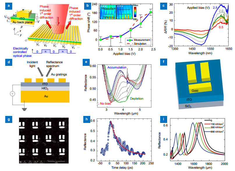
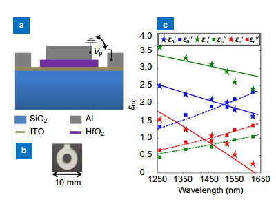
Figure reproduced from ref.119, American Chemical Society.\omega _{\rm{p}}^2 = \frac{{N{e^2}}}{{{\varepsilon _0}{m^{\rm{*}}}}}, {\varepsilon '_{\rm{r}}}(\omega ) = {\varepsilon _\infty } - \frac{{\omega _{\rm{p}}^2}}{{{\omega ^2} + {{\mathit{\Gamma}} ^2}}}, In one example of a modulator, as shown in Figs. 4(a) and 4(b)120, the ITO layer is used as the top electrode and the voltage is applied directly to the ITO layer. Formation of a 5 nm depletion (under positive voltage Vp=10 V) and accumulation layer (under negative voltage Vp=10 V) is assumed. The rest of the ITO layer remains un-changed with the value of the blue markers (voltage Vp=0 V).
\rho = \frac{1}{\sigma } = \frac{{{m^{\rm{*}}}}}{{N{e^2}\tau }}. In order to tune the electron density in the ITO layer, different structures have been proposed. As shown in Fig. 2, a metal-oxide-semiconductor heterostructure with ITO as the active material is used to realize the tunability with the DC voltage applied to the two gold electrodes119. Since the ITO is conductive, the electrons with negative charges are absorbed toward the positive electrode and accumulated in the conductive oxide-dielectric interface. The simulation and measurement results showed that the electron density was increased from N=1×1021 cm-3 to N=2.8×1022 cm-3 in an electron accumulation layer of (5±1) nm layer of ITO, while the DC voltage increased from 0 to 2.5 volts.
{\tilde \varepsilon _{\rm{r}}}(\omega ) = {\varepsilon '_{\rm{r}}}(\omega ) + {\rm{i}}{\varepsilon ''_{\rm{r}}}(\omega ) = {\varepsilon _\infty } - \frac{{\omega _{\rm{p}}^2}}{{{\omega ^2} + {\rm{i}}\omega {\mathit{\Gamma}} }}, The electrical conductivity σ and resistivity ρ are given by:
Transparent conductive oxides (TCO) are materials optically transparent and electrically conductive. These materials have been widely used in photovoltaics, organic light emitting diodes (OLEDs), displays, and electro-optics devices in general110-114. Recently, the tunable property of TCOs such as ITO has attracted great attention for its application in metasurface and nano-optics.
{\varepsilon ''_{\rm{r}}}(\omega ) = \frac{{{\mathit{\Gamma}} \omega _{\rm{p}}^2}}{{\omega ({\omega ^2} + {{\mathit{\Gamma}} ^2})}}. {\mathit{\Gamma}} = \frac{1}{\tau } = \frac{e}{{\mu {m^{\rm{*}}}}}, The same principle is used to achieve tunability for the amplitude of the reflected light85 as shown in Fig. 5(d). However, since the ITO layer (6 nm) is on top of the insulator layer (20 nm), the electric field and DC voltage are opposite compared to previous design and the voltage is applied directly to the ITO layer. Strong absorption modulation is shown when the ITO is operated in the ENZ spectrum [shown in Fig. 5(e)].
The changes in refractive index versus wavelength at different bias voltages are shown in Fig. 3. The refractive index decreases and the extinction coefficient increases as the bias voltage increases. The change in refractive index due to bias voltage is much larger at higher wavelengths as it is getting closer to epsilon-near-zero. Change of the refractive index can reach 1.39 (around 70%) at 800 nm, which is extremely large compared to other types of materials.
Furthermore, it was found that there is no change in refractive index when DC voltage was applied reversely since the opposite electric field would result in the formation of the depletion layer. When the thickness of the ITO layer is reduced by half, the same change in the refractive index was observed for the same electric field because the change is only due to the accumulation of electrons in a thin layer at the ITO-SiO2 interface.
The epsilon-near-zero (ENZ) wavelength (λENZ) is the wavelength at which the real part of the dielectric constant passes through zero115-117. If the imaginary part of the permittivity is zero or very small at the same wavelength, the refractive index would become close to zero, much smaller than the refractive index of vacuum. Although common materials i.e. metals have {\tilde \varepsilon _{\rm{r}}} at plasma frequency, the imaginary part of the permittivity is quite large. However, in transparent conductive oxides, the ENZ wavelength can be tuned in the visible or near infrared spectrum with a very small value of the imaginary part of the permittivity due to low loss 118. The epsilon-near-zero is given by:
![Figure 5. Tunable metasurfaces using ITO as an active layer.]()
Tunable metasurfaces using ITO as an active layer.
(a) Schematic of the tunable metasurface which consists of a quartz substrate, gold backplane, and a thin ITO film followed by a thin alumina film on which gold stripe nanoantenna array is patterned on. (b) Measured relative reflectance change from the metasurface for different applied voltages. (c) Measured and simulated phase shift as a function of applied bias for the applied voltage. The black lines show the cross-section for analyzing the phase. (d) Device schematic showing an electrically-tunable ITO film clamped between an HfO2-coated Au substrate and an array of Au strips. With positive and negative electric biases, the carrier concentration of ITO can be decreased (depletion) or increased (accumulation), leading to changes in the optical properties of the ITO. (e) Reflectance spectra were taken from the device measured using an FT-IR microscope. The red, blue, and green curves denote the reflectance spectra under 0 V for no bias, −5 V for accumulation, and +5 V for depletion, respectively. The grey curves represent reflectance spectra for intermediate voltages with an incremental step size of 1 V. (f) Schematic structure of the meta-molecule and (g) top-view small-scale SEM image of the metamaterial. (h) Measured reflectance changes of a 1550 nm probe laser as a function of delay time between pump and probe pulses. The red solid line is the exponential fit to the data. (i) The calculated reflectance spectrum of the metamaterial with different pump intensity by the finite element method. Figure reproduced from: (a–c) ref.47, American Chemical Society; (d, e) ref.85, Creative Commons Attribution 4.0 International License; (f–i) ref.59, Creative Commons Attribution 4.0 International License.n(\omega ) = \sqrt {\frac{{\sqrt {{{\varepsilon '}_{\rm{r}}}^2 + {{\varepsilon ''}_r}^{\;2}} + {{\varepsilon '}_{\rm{r}}}}}{2}} , By changing the carrier concentration, the plasma frequency changes, thereby changing the dielectric constant. The complex refractive index is given by:
As shown in Fig. 5(h), the measured reflectance peak at 1550 nm (center of the transparency window) is tuned by increasing the delay time between the pump and probe pulses by using the femtosecond laser pump and probe method. The refractive index n of the polycrystalline ITO is given by59:
n = {n_0} + {n_2}I = {n_0} + \frac{{3Re_\chi ^{(3)}}}{{4c{\varepsilon _0}n_0^2}}{I_0}, where c is the speed of light in vacuum. As shown in Eq. (10), changing plasma frequency will change the epsilon-near-zero wavelength. If the electron density N increases, according to Eq. (3), the plasma frequency increases and the epsilon-near-zero wavelength decreases. According to Eq. (8), when the {\varepsilon '_{\rm{r}}} , the real part of the permittivity, becomes zero, refractive index n becomes the minimum possible value of \sqrt {{{\varepsilon ''}_{\rm{r}}}/2} epsilon-near-zero wavelength. However, as seen from Eq. (5), the imaginary part of the permittivity {{\varepsilon ''}_{\rm{r}}} is correlated with loss and increases as the plasma frequency increases.
![Figure 3. The refractive index (n) and extinction coefficient (k) in a 5 nm accumulation layer, extracted data from the ellipsometry measurements.]()
The refractive index (n) and extinction coefficient (k) in a 5 nm accumulation layer, extracted data from the ellipsometry measurements.
Figure reproduced from ref.119, American Chemical Society.Fitting of the real and imaginary part of the dielectric constant of the active ITO layer is shown in Fig. 4(c). When a negative voltage is applied to the ITO film, positive carriers (holes) accumulate at the ITO-HfO2 interface. On the other hand, under positive bias, the active layer will be depleted and negative carriers (electrons) would accumulate at the interface. The carrier concentrations for the accumulation and depletion states are calculated as Na=3.23×1021 cm-3 and Nd=1.57×1021 cm-3, respectively. By comparison with the original value N0=3.05×1021 cm-3, we can see that the free carriers are more easily depleted than accumulated.
where τ is the scattering time, e is the electron charge, μ is the electron mobility, ε0 is the vacuum permittivity, m* is the effective electron mass, and N is the carrier (electron/hole) concentration. The real and imaginary parts of the permittivity are given by:
It could be seen from Eq. (8) that changing the dielectric constant will change the refractive index. The properties of ITO film, i.e. the conductivity and carrier concentration, could be controlled during the film deposition, which in turn will change the dielectric constant and the tunability of the refractive index of ITO film.
ITO is a conducting material and has free electrons. It is modeled using the Drude model:
{\lambda _{{\rm{ENZ}}}} = \frac{{2{\rm{ \mathsf{ π} }}c}}{{{\omega _{{\rm{ENZ}}}}}} = \frac{{2{\rm{ \mathsf{ π} }}c}}{{\sqrt {\frac{{\omega _{\rm{p}}^2}}{{{\varepsilon _\infty }}} - {{\mathit{\Gamma}} ^2}} }}, ITO film can also have its properties tuned by optical excitation59, 60, 121. Y. Zhu, et al. reported that under the excitation of a femtosecond laser with a wavelength at the optical communication range, the hot-electron injection from gold to ITO film enhanced nonlinearity of polycrystalline ITO59. Furthermore, the field reinforcement provided by plasmonic resonances also contributes to the nonlinearity enhancement of ITO.
where n0 and n2 are linear and nonlinear refractive indices of poly-crystalline ITO, respectively, and {3Re_\chi ^{(3)}} is the real part of the third-order nonlinear susceptibility of polycrystalline ITO. Since n2 is negative in polycrystalline ITO, the linear refractive index of polycrystalline ITO decreases under the excitation of a pump laser122. Therefore, when there is a zero delay between probe and pump pulses, the central wavelength of the transparency window shifted towards the short-wavelength direction. Hence, the reflectance of the 1550 nm probe laser increased under excitation of the pump laser. The central wavelength of the transparency window could be tuned by 86 nm [shown in Fig. 5(i)].
![Figure 4. The tunability of ITO in a multilayer modulator.]()
The tunability of ITO in a multilayer modulator.
(a) Cross section of the multilayer ITO modulator. (b) Picture of the fabricated modulator. (c) Solid and dashed lines are from further fitting by the Drude model. Figure reproduced from ref.120, Optical Society of America.{\tilde n^2} = {(n + {\rm{i}}\kappa )^2} = {\tilde \varepsilon _{\rm{r}}}{\tilde \mu _{\rm{r}}}, where {\tilde n} is the complex refractive index, n is the ordinary refractive index, κ is the extinction coefficient, {\tilde \varepsilon _{\rm{r}}} is the complex relative permittivity (dielectric constant), and {\tilde \mu _{\rm{r}}} is the complex relative permeability. Since ITO is a non-magnetic material at optical frequencies, its relative permeability is very close to 1. Hence the refractive index and extinction coefficient is given by:
where {\tilde \varepsilon _{\rm{r}}} is the material permittivity, {\varepsilon _\infty } is the high frequency permittivity, ω is the angular frequency, ωp is the plasma frequency, and Γ is the damping rate. The plasma frequency and the damping rate are defined as:
Combination of tunable ITO layer with metal plasmonic resonators has been used to design different active metasurfaces47, 59, 60, 85, 86, 121. As shown in Fig. 5(a), a reflective gold plasmonic resonator is used to modulate the amplitude and phase of the electromagnetic wave47. Each unit cell has one gold resonator on top and one gold backplate at the bottom. Between them, there are two layers of Al2O3 insulator and ITO with a thickness of 5 nm and 20 nm, respectively. By applying a DC bias voltage, an electric field is created between the top gold resonator and bottom gold plate and a charge accumulation layer is formed in the ITO film at the interface with the Al2O3 insulator. This charge accumulation layer causes a huge change in the refractive index of ITO film which in turn changes the phase and amplitude of the reflected electromagnetic waves. Since the change in refractive index happens only in ~5 nm thick layer of the ITO, the largest change in the phase of the reflected wave occurs near the resonance of the plasmonic structure, whereas the loss is usually very high and the efficiency is very low. The relative reflectance change and phase change are shown in Figs. 5(b) and 5(c). The maximum relative reflectance change of 30% and phase change of 184° are obtained at 2.5 V DC bias. Relative reflectance change is defined as the ratio of reflectance change due to applying bias [ΔR=R(V)-R(0)] to that without an applied bias [R(0)].
Ferroelectric materials
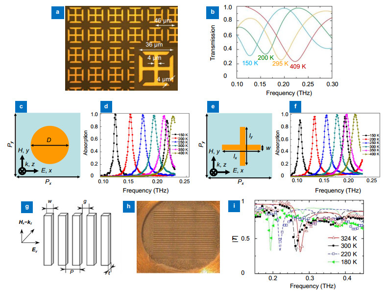
K = \frac{{{\eta _{\rm{r}}}}}{{\tan \delta }}. ![Figure 7. Thermal tuning of ferroelectric materials in active metamaterials.]()
Thermal tuning of ferroelectric materials in active metamaterials.
(a) Microscopic image of the metamaterial consisting of a gold electric split-ring resonator array fabricated on an STO substrate and (b) measured normalized THz transmission amplitude spectra through the metamaterial. (c) and (e) show the unit cell of the proposed frequency tunable metallic ring and cross absorbers, respectively and (d) and (f) show the calculated absorption spectra of the proposed frequency tunable metallic ring and cross absorbers at different temperatures, respectively. (g) Schematic view of the structure. (h) Scanning electron microscopy image of the metamaterial. (i) Theoretical and experimental transmission spectra. Figure reproduced from: (a, b) ref.52, Optical Society of America; (c–f) ref.53, Optical Society of America; (g–i) ref.130, Springer Nature.
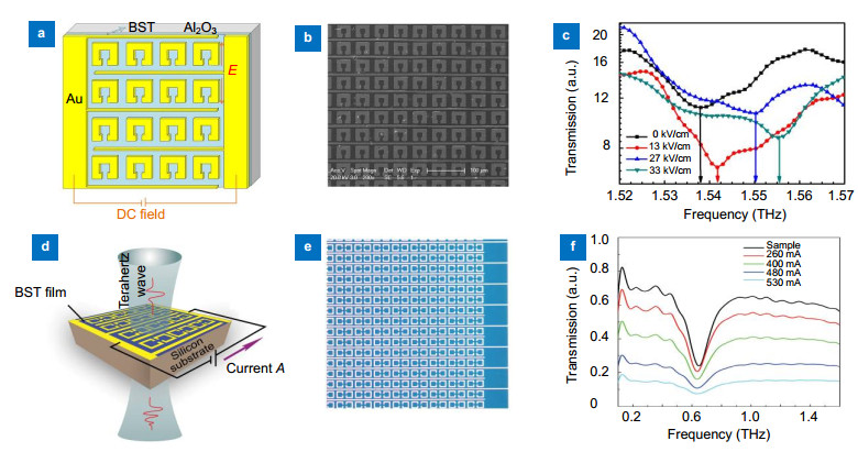
Tunable metasurface has also been demonstrated using BST as the tunable ferroelectric material51, as shown in Figs. 8(a) and 8(b). Common split ring resonators (SRR) are designed to have the desired resonance frequency and separate interdigital electrodes are added to apply DC voltage and electric field to tune the BST layer beneath the SRR resonator specifically in the area in the vicinity of the SRR gaps. As shown in Fig. 8(c), by increasing the electric field from 0 to 33 kV/cm, the resonance frequency is increased from 1.52 THz to 1.57 THz. This approach is straightforward and adaptable to other frequencies. This type of electrical tuning method is simpler and easier for practical applications.
{\eta _{\rm{r}}} = \frac{{\varepsilon (0) - \varepsilon ({E_0})}}{{\varepsilon (0)}}. Most common ferroelectric materials used to design tunable metasurfaces are barium strontium titanate (BST), barium titanate (BTO)125, lithium niobate (LiNbO3)61, 126-128, and strontium titanate (STO)52, 53, 129-138. Electrical and thermal tuning of ferroelectric materials is two most commonly used approaches for realizing tunable metasurfaces by changing the dielectric constant of ferroelectric materials in paraelectric phase.
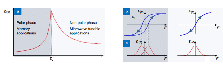
In ferroelectric materials, the crystal structure lacks a center of symmetry. As a result, they have a spontaneous electric polarization that can be reversed by the application of an external electric field123. Tunability, η, of an electrically tunable ferroelectric material, is defined as the ratio of its permittivity at a zero applied electric field to its permittivity at a specific non-zero applied electric field E0124:
The relative permittivity of a ferroelectric crystal is temperature dependent and undergoes a phase transition as the temperature is increased. The crystal possesses a spontaneous polarization below the phase transition temperature known as the Curie temperature (TC).
![Figure 6. Phase transition in ferroelectric materials.]()
Phase transition in ferroelectric materials.
(a) Temperature dependence of the dielectric constant of a ferroelectric material. The material transitions from a polar to a non-polar phase at the Curie temperature Tc. (b, c) The corresponding polarization and dielectric constant as a function of applied field below and above Tc. Figure reproduced from: (a–c) ref.124, AIP Publishing.The performance of a tunable dielectric material is generally evaluated using the figure of merit (K):
A new active BST-silicon hybrid metamaterial with aluminum square split-ring resonators (SRRs) was reported139. Experimental design with the illustration of the device and the microscopic image of the device are shown in Figs. 8(d) and 8(e). Under the optical excitation, a conductive silicon layer is generated beneath the 150 nm thin BST layer where the electron density was enhanced due to carrier generation. The electrons would migrate into the BST film from silicon layer and get trapped there until a new equilibrium is reached and leads to a large increase of the absorption coefficient in BST film. Figure 8(f) shows the measured amplitude transmission with the different electric current. An LC resonance is observed at 0.64 THz at zero gate current. The amplitude modulation depth reaches ~70% at the resonance frequency and ~79% at 1 THz when the current is increased to 530 mA.
![Figure 8. Electrical tuning of the ferroelectric material in active metamaterials.]()
Electrical tuning of the ferroelectric material in active metamaterials.
(a) Schematic view of the SRR unit cell and the IDE patterns. (b) SEM image of the SRRs and the IDE patterns. (c) Transmission spectra of the metamaterial at various electric fields. (d) Schematic illustration of the metamaterial and experimental design. (e) Microscopic image of the fabricated BST–silicon hybrid metamaterial. (f) Measured transmission amplitude spectra of the BST–silicon hybrid metamaterial at various gate currents. Figure reproduced from: (a–c) ref.51, AIP Publishing; (d–f) ref.139, John Wiley and Sons.The variation in dielectric constant with temperature is most pronounced near the Curie temperature resulting in a considerably large permittivity and tunability. It is thus desirable for tunable applications to operate the crystal just above the Curie temperature to take advantage of the high tunability while avoiding losses associated with the hysteresis of the ferroelectric phase.
Relative tunability can be defined as:
\eta = \frac{{\varepsilon (0)}}{{\varepsilon ({E_0})}}. A few examples of thermal tuning of ferroelectric materials in metasurfaces are shown in Fig. 7. A planar terahertz metamaterial made of gold split-ring resonators array is fabricated on a single-crystal strontium titanate (SrTiO3) substrate [Fig. 7(a)]. As shown in Fig. 7(b), the resonance frequency of the metamaterial is tuned over 43% by changing the temperature from 409 K to 150 K. As the temperature changes the refractive index of the STO substrate changes (Δn~11), which leads to change in the resonance frequency. Figures 7(c) and 7(e) show two absorber metasurfaces which have 17 μm thick STO film between the gold ring/cross resonators and back plate. The resonance frequency in the ring resonator is increased from 0.126 THz at 150 K to 0.227 THz at 400 K, which is up to 80% frequency tuning [shown in Fig. 7(d)]. In the cross resonator, the resonant frequency is increased from 0.116 THz at 150 K to 0.208 THz at 400 K and a 79% frequency tunability is obtained [shown in Fig. 7(f)]. In Figs. 7(g) and 7(h), a negative permeability metamaterial which is made of STO bars (width w=42.5 μm) with a thickness of t=52 μm is shown. The theoretical and experimental magnitudes of the transmittance are shown in Fig. 7(i). The resonance frequency has been tuned from 0.2 THz at 180 K to 0.28 THz at 324 K.
Graphene
Graphene, a two-dimensional (2D) material with unprecedented properties has attracted tremendous attention for future electronic and photonic applications since it was discovered in 2004140. Graphene has a low carrier density of states near the Dirac point, hence its Fermi level can be tuned with small bias gate voltage141, 142. This phenomenon leads to novel ways of manipulating the interaction between light and matter. Moreover, it has high carrier mobility, which makes it a desirable candidate for plasmonic material with relatively low loss50.
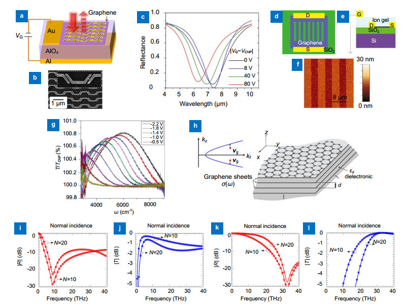
Another tunable hyperbolic absorber metamaterial at THz spectrum made by stacking graphene sheets and dielectric layers is shown in Fig. 9(h)162. The dielectrics are 100 nm thick SiO2 films, and the number of the layers is N. The surface conductivity σ(ω, μc) of a monolayer graphene could be tuned by chemical potential (μc), which is controlled by electrostatic biasing. By applying a voltage to the graphene layers μc is increased from 0 to 0.4 eV. As it could be seen the absorbance resonance of the metasurface with 10 and 20 layers is increased [shown in Figs. 9(i)-9(l)].
Due to these unique properties, graphene has been used to design different types of tunable metasurfaces from THz to near-IR143-145. Majority of these metasurfaces employ either metal or dielectric resonators with a layer of graphene to realize the tuning function50, 87, 88, 146-156, while some metasurfaces use the patterned graphene as plasmonic resonator directly49, 89, 90, 157-161. There are also metasurfaces which use multilayers of graphene with different materials, such as dielectric or ferroelectric materials, to achieve tunability without using any nanostructured resonators162-166.
Figures 9(d) and 9(e) show schematics of a tunable absorber metasurface over a broad terahertz frequency range composed of graphene micro-ribbon arrays. Figure 9(f) is the AFM image of the fabricated graphene micro-ribbon array sample. The carrier concentration in the graphene monolayer is controlled using the Vg applied to the top gate on ion-gel. As can be seen in Fig. 9(g), in the transmission spectra in mid-IR, T/TCNP, the resonance frequency of the metasurface shifts to lower wavelength and higher frequency by increasing Vg from -0.5 to -2.2 V.
![Figure 9. Tunable metamaterials using graphene as the active material.]()
Tunable metamaterials using graphene as the active material.
(a) Schematic view of the ultrathin optical modulator based on a tunable metasurface absorber. (b) SEM image of the metasurface on graphene (a zoomed-in view of a portion of the metasurface is shown in the inset). (c) Normalized measured reflection spectra of the metasurface absorber for different gate voltages (VG−VCNP=VCNP is the gate voltage when the concentrations of electrons and holes in the graphene sheet are equal) to the reflection spectra from a 300 nm Al film on the same silicon substrate. Schematic (d) top and (e) side view of a typical graphene micro-ribbon array on a Si/SiO2 substrate, (f) AFM image of a graphene micro-ribbon array sample with a ribbon width of 4 mm and a ribbon and gap width ratio of 1:1, and (g) relative mid-infrared transmission spectra (T/TCNP) of the graphene ribbon array as gate voltage (Vg−VCNP) varies from-0.3 to 2.2 V (the voltages corresponding to the un-labeled lines, starting with the red line and alternating downwards, are 2.0 V, 1.6 V, 1.2 V, 0.7 V and 0.3 V). (h) Schematic view of the composite multilayer material made by stacking graphene sheets and dielectric layers (under certain conditions, it exhibits hyperbolic-like iso-frequency wavevector dispersion which is shown in the inset, where Vg indicates the direction of the group velocity), (i) reflection and (j) transmission for a finite thickness graphene-silica multilayered HM, at normal polarization, calculated by transfer matrix method (solid lines) and EMA (circles) when graphene layers are unbiased, i.e., μc=0 eV, and (k) reflection and (l) transmission versus frequency, for the same set of parameters, except that now graphene layers are biased with μc=0.4 eV. Figure reproduced from: (a–c) ref.88, American Chemical Society; (d–g) ref.49, Springer Nature; (i–l) ref.162, Optical Society of America.
Figures 9(a) and 9(b) show a tunable perfect absorber metasurface composed of optical antennas on graphene as shown in ref.88. Aluminum (Al) is used as the resonators, gate pad, and bottom plate. Aluminum oxide is used as the dielectric spacing between the bottom Al and top graphene monolayer. By applying DC voltage to the graphene via gate pad, the absorber is switched on and off the critical coupling condition, which causes a modulation depth of up to 95% [shown in Fig. 9(c)]. Since the resonant frequency of the metasurface is controlled by the dimensions of the unit cells, it could be scaled from the near-infrared to the terahertz by changing the metasurface and cavity dimensions.
Phase change materials
Chalcogenide phase change materials composed of alloys of Germanium (Ge), Antimony (Sb), and Tellurium (Te) can be easily transited between disordered-amorphous state and ordered-crystalline state by a heat-quench cycle. They have been used in optical storage and non-volatile memory by exploring the change in the optical or electronic properties. More recently, this GST based chalcogenide material has gained a lot of interest as a new platform for tunable and reconfigurable metasurfaces due to their pronounced contrast of dielectric properties, high switching speed, and good thermal stability. When the chalcogenide is heated above the glass transition temperature by a laser pulse or electronic excitation, they produce a thermal nature transition process occurring by nucleation and crystallization growth. Re-amorphization is achieved by heating the material above the melting temperature followed by rapid cooling. The large optical/electronic contrast between the two states is attributed to atom re-arrangement.
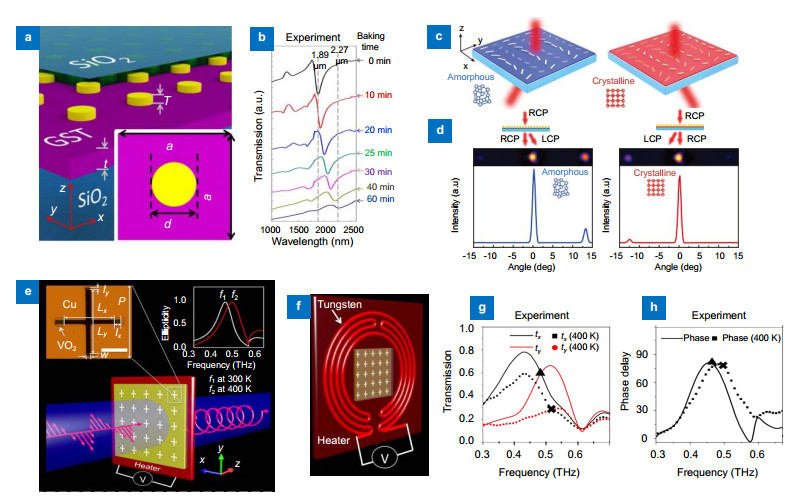
![Figure 10. Tunable metamaterials using GST as the active material.]()
Tunable metamaterials using GST as the active material.
(a) Schematic diagram of the plasmonic metamaterial which has an array of gold nano-disks on a thin layer of GST (T=40 nm, t=20 nm, d=280 nm, a=1.2 µm). (b) Measured normalized transmission spectra of continuously tuning of the hybrid plasmonic metamaterial measured at different baking time during the crystallization process. (c) The schematic view of the active plasmonic metasurface for beam switching which consists of a 50 nm thick GST-326 layer underneath a geometric phase metasurface for beam switching (two types of nano-antennas A and B with different plasmon resonances are alternated line-wise), when the active layer is in the amorphous phase, only type A rods interact with the incident light and deviate the beam to the left and when the active layer is in the crystalline phase, only type B rods interact with the incident light and deviate the beam into the opposite direction due to their relative orientation (right). (d) Infrared camera images and intensity plots of the beam transmitted by the active metasurface in the amorphous (left) and crystalline (right) state. (e) Schematic view of switchable THz quarter-wave plate design. The top left inset is a microscope image of one unit cell in the fabricated sample (P=150, Lx=90, Ly=124, lx=9, ly=5 and w=9 μm, and the scale bar is 50 μm). The top right inset is the simulated ellipticities of the output THz waves. (f) Schematic backside view of the resistive heater with a square aperture (6 mm × 6 mm) milled at the center to allow THz to pass through. (g) Measured transmission spectra along two slots at 300 K (solid line) and 400 K (dot line). (h) Measured the phase difference between y- and x-axes at 300 K (solid line) and 400 K (dot line). Figure reproduced from: (a, b) ref.92, Optical Society of America; (c, d) ref.167, Creative Commons Attribution 4.0 International License; (e–h) ref.96, Creative Commons Attribution 4.0 International License.Vanadium dioxide (VO2), another phase change material, also attracted much attention and has featured prominently in the tunable metamaterial field due to its special property of phase transition from insulator to metal and vice versa as temperature changes. Their phase transition temperature is lower compared with chalcogenide glass, making it easy to be thermally, electrically, or optically stimulated. When phase changes between two states, VO2 is accompanied by significant changes in optical and electronic properties. It is a suitable functional material for many optoelectrical applications, such as active polarizer in near-infrared region95, tunable absorber97, 187, 188, tunable switching189, 190, beam steering191, switchable quarter wave plate (QWP) in THz96, 192, and active nanoantennas for tuning THz resonance193-195. By hybridizing metasurfaces with VO2, an ultrathin switchable THz QWP with a switching range of 34 GHz was experimentally demonstrated96. Fig. 10(e) shows a schematic of the switchable QWP, which is composed of ultrathin asymmetric cross-shaped resonator arrays with VO2 pads inserted at the end of the cross-shaped resonators. A linear normal incident THz wave polarized at θ = 45° to the two slots is converted into a circularly polarized light. The inserted VO2 is able to change the effective length of the metal resonators in the metasurface through the phase transition controlled by a resistive heater shown in Fig. 10(f). Through the VO2 phase transition, the operating frequency of the QWP is switched between f1=0.468 THz and f2=0.502 THz, as illustrated in Figs. 10(g) and 10(h).
The thin GST layer was introduced into the metal-dielectric-metal configuration for realization of a tunable plasmonic resonance168-170, absorber98, 171-173, reflector174, circular dichroism175, 176, chirality177, 178 and negative index metamaterials179. A non-volatile all-optical modulation of resonance in infrared is reported as a broadband switch through the combination of chalcogenide glass phase change medium with nanostructured plasmonic metamaterials180. The single pulse laser excitation was used to homogenously phase transition across the large areas of the hybrid metamaterial devices, which bring dramatic changes in the optical transmission and reflection characteristics. Similarly, as shown in Fig. 10(a), non-volatile tuning of gold nano-disk resonance is achieved over a broad spectral range of 500 nm (1.89 μm to 2.27 μm) by including thin GST layer as a refractive index tunable environment92. Transmission spectra of the hybrid plasmonic crystal are measured at different intermediate phases and shown in Fig. 10(b). With an increasing baking time, a more metal-like portion generated in the phase-change thin film is seen due to a red-shift of the lattice resonance. Specifically, at 1.89 μm wavelength, the transmittance is increased from 16% (black curve) to 72% (blue curve) after baking for 20 min. Laser-induced reversible switching of infrared nanoantenna resonances was demonstrated with a thin layer of GST surrounding the Al nanostructure181, 182. Furthermore, all-optical, non-volatile, and reversible switching of phonon-polaritons is realized by controlling the structural phase of GST thin layer on top of crystal quartz183. As shown in Fig. 10(c), with the integration of plasmonic metasurfaces and the phase change material, active metasurfaces were achieved for dynamic beam switching and bifocal zoom lensing167. Two different sets of plasmonic antenna elements A and B provide beam refraction in opposite directions but are spatially staggered within one light interaction area on top of a thin GST layer. The lengths for A and B type antennas have been chosen such that their respective plasmon resonance wavelengths match the operating wavelength either in the amorphous or crystalline PCM state. As a result, each set of plasmonic antennas strongly interacts with the incident light at a certain operating wavelength. The resulting images for right-handed circular polarized (RCP) light illumination from the infrared camera and intensity plots of the beam transmitted by the active metasurface are shown in Fig. 10(d). When the GST is in its amorphous state, antenna set A interacts with the incident light and refracts the cross-converted portion of the incoming beam, left-handed circular polarized (LCP) to the right side of the non-converted RCP part. For crystalline GST, the incident beam interacts with antenna set B, thus, the converted portion is refracted to the opposite direction.
Chalcogenide phase change material has also emerged as a paradigm for the realization of non-volatile, all-optical dielectric metamaterials, presenting Mie resonances with low-loss as opposed to noble metals184. Phase change GST rods were patterned to a different size in their amorphous and crystalline states for the realization of tunable gradient metasurfaces185. Specifically, at low fluence, the femtosecond laser pulses only melt a thin layer of amorphous GST film, which leads to partial crystallization state through an interfacial solidification process186. Utilization of diffraction-limited optical writing system, various reconfigurable metasurfaces, and photonics devices were demonstrated in the thin GST film97. With this capability, reconfigurable phase change photomask for 3D optical lithography and waveguides for optical trapping were demonstrated93, 94.
Liquid crystals (LCs)
The ability of a metamaterial absorber array hybridized with liquid crystals to work as a spatial light modulator in THz wavelengths has been reported108. As shown in Fig. 12(e), the orientation of the LC molecules is electronically controlled and used to tune the resonance frequency of the absorber metamaterial. The measured and numerical simulated frequency dependent absorptivities in the two biasing conditions for an individual pixel are shown in Fig. 12(f). Measured absorptivities are in good agreement with numerical simulations and show a modulation performance of the reflectivity of 75%.
Liquid crystals are often used as an ambient or dielectric material in the metasurfaces. As the phase of the LC is changed, its dielectric constant and refractive index changes as well. Various types of active metasurfaces employ different mechanisms for tuning the liquid crystal, i.e. applying electric field99, 100, 108, 197-213, magnetic field67, 68, optical pumping101, 214, or thermal heating102, 103, 109, 215, 216.
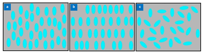
![Figure 11. Liquid crystal molecules orientation and periodicity in (a) smectic, (b) nematic, and (c) isotropic phases.]()
Liquid crystal molecules orientation and periodicity in (a) smectic, (b) nematic, and (c) isotropic phases.
Aggregation-free elastic self-alignment of nanorods dispersed in LCs and their realignment by shearing and magnetic fields have been experimentally demonstrated67. The anisotropic fluids in both columnar hexagonal and nematic LC phases impose a nematic-like orientational ordering of gold nanorods (GNRs) with the GNRs aligning along the LC director n (a unit vector describing the average local orientation of cylindrical micelles forming the LC). As shown in Figs. 12(j) and 12(k). The diameter of micelles is 2-3 nm and gold nanorods have a diameter of 15-25 nm and length of ~50 nm. Polarized surface plasmon resonance spectra taken from samples with magnetically realigned n show that the LC matrix aligns GNRs along n [Fig. 12(l)] and GNR orientation in the nematic fluid can be controlled by magnetic fields (11.7 T in the experiments) via switching of n.
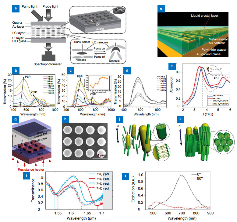
New types of light-driven plasmonic color filters by overlaying photoresponsive liquid crystals on gold annular aperture arrays are designed and experimentally demonstrated101. Figure 12(a) shows the schematic of the sample structure and experimental setup for optical spectra measurement. Upon UV irradiation, the photoresponsive LC molecules can undergo a reversible photoisomerization between the trans (rod-like shape) and the cis (bent shape) molecular forms (shown in magnified part II), which disrupts the local order of LC molecules and makes the system optically active. As shown in Figs. 12(b) and 12(c), there are two obvious transmission bands for each color filter with different aperture size: one is located in a wavelength range of 500-600 nm and the other one in 700-800 nm. They are attributed to coherent interactions between two main plasmons: cylindrical surface plasmons (CSPs) and planar surface plasmons (PSPs). Figure 12(d) shows a typical evolution of the transmission spectra as a function of time under the UV pump for the gold structure with an aperture size of 120 nm. By UV light shining, the trans-isomer transforms into the cis-isomer, which disrupts the local order of the host nematic and forms an isotropic phase. This order change generates a photoinduced refractive index modulation and results in a ~18% decrease in the peak transmission intensity.
Figure 12(g) shows an all-dielectric metasurface composed of silicon nanodisks integrated into the liquid crystal. The individual nanodisk height and diameter and liquid crystal height are 220 nm, 606 nm, and 170 μm, respectively. Resistance heating of the silicon handle wafer is used to control the temperature and phase of the LCs. Figure 12(h) shows the SEM image of the Si nanodisk metasurface. Liquid crystal is covered by a glass substrate that is coated with a functional layer of poly (vinyl alcohol) (PVA) with the preferred alignment of the liquid crystal in the x-direction. Figure 12(i) shows the measured normalized transmittance spectra at room temperature with red and cyan solid line for x- and y-polarized incident light, respectively. Heating the sample above the LC phase transition temperature (Tc ~58 ℃) induces a pronounced blue-shift for the electric resonance and a slight red-shift for the magnetic resonance, resulting in identical spectra for x- and y-polarization (red and cyan dashed lines) as the LC switches from its nematic to its isotropic phase.
Liquid crystals (LCs) are mesophase materials which have properties between liquids and solid crystals. A liquid material has uniform properties in all directions, called isotropic. However, a crystalline solid is anisotropic, meaning it has different optical, electrical, conductivity, and other properties in different directions and its molecules are in a periodic arrangement in one spatial direction. LCs physically behave like liquids but are anisotropic specifically in optical properties like solid crystals196. They have mainly used in two different phases named nematic and smectic shown in Fig. 11. In nematic phase, the molecules have the same orientation but are free to drift around and have no periodicity. In the smectic phase, the molecules have the same orientation and are arranged in layers with periodicity. The individual layers in the smectic phase can slip over each other in a manner similar to graphite. Moreover, by increasing the temperatures, the molecules in LCs would be oriented arbitrarily, turning to an isotropic phase, as illustrated in Fig. 11(c).
![Figure 12. Tunable metamaterials using LCs as the active material.]()
Tunable metamaterials using LCs as the active material.
(a) Schematic of the sample structure and experimental setup. The inset Ⅰ shows the fabricated square pattern of gold AAAs. The inset Ⅱ shows the working mechanism of the optical driving process. The (b) theoretically calculated and (c) experimentally measured transmission spectra of color filters with different aperture sizes. The inset in (c) shows the measured FWHM of corresponding transmission peaks. (d) The evolution of the transmission spectra as a function of time under the UV pump for the color filter with an aperture size of 120 nm. (e) Schematic view of metamaterial absorber array covered with LC designed for the experiment. (f) Comparison of the measured frequency-dependent absorptivities (A=1−R) in the biased (red continuous line) and unbiased conditions (blue continuous line) with those from numerical calculations (dashed lines). The inset shows the calculated percentage modulation factor as a function of the liquid crystal losses. (g) Schematic view of the silicon nanodisk metasurface integrated into an LC cell. The silicon nanodisk sample is immersed in the LC, and the cell is covered by a layer of brushed PVA for alignment of the LC. A resistor heater is mounted on the backside of the silicon wafer. (h) Scanning electron micrograph of the silicon nanodisk metasurface. (i) Measured normalized transmittance spectra. (j) Schematic illustration of gold nanorods alignment in the nematic LC and (k) gold nanorods alignment in a columnar hexagonal lyotropic LC phase. (l) Experimental extinction spectra of gold nanorods in a nematic LC realigned by a magnetic field. Figure reproduced from: (a–d) ref.101, John Wiley and Sons; (e, f) ref.108, John Wiley and Sons; (g–i) ref.109, American Chemical Society; (j–l) ref.67, American Chemical Society.Semiconductors
Semiconductors are the key materials for electronics and photonics. The ability to tune the carrier concentration and the refractive index of semiconductor material renders them promising perspectives for tunable metasurface and metadevices. Recently there have been numerous reports on tunable metasurfaces using a semiconductor as the tunable material for optical tuning58, 217-228 electrical tuning107, 139 and the combination of both electrical and optical excitation155, 229.
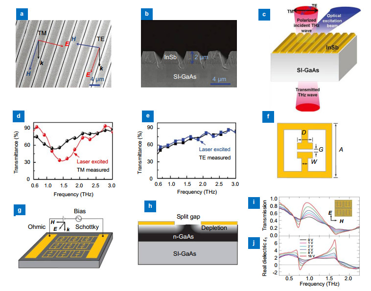
An active metadevice capable of efficient control of THz radiation is proposed using GaAs as the tunable semiconductor107. As shown in Figs. 13(f) and 13(g), an array of gold split ring resonators are fabricated on a 1 mm thick n-type GaAs layer grown on a semi-insulating GaAs wafer. Fig. 13(h) shows the working principle of the metadevices through controlling depletion of the carriers in the n-GaAs layer in the gap region. Tuning performance of the metadevice when the polarization of the THz electric field is perpendicular to the DC bias lines is shown in Figs. 13(i) and 13(j) as a function of gate voltage bias. As the reverse bias increases, the resonances in the transmission spectra narrow and increase in amplitude. At 0.72 THz, a 50% relative intensity change of transmission is observed at a reverse gate bias of 16 V. Hence, this device could be used as a reasonably efficient narrowband THz switch/ modulator.
An optically tunable metasurface is presented using InSb as both the metasurface and the active media58. A deep subwavelength InSb 1D grating structure was used as the basic metasurface structure. Figures 13(a) and 13(b) show the planar and cross-sectional SEM images of the fabricated InSb grating and Figure 13(c) illustrates the characterization of the active InSb based metasurface at THz wave incidence with optical tuning by another laser (405 nm). The transmittance of TM and TE polarized THz waves are shown in Figs. 13(d) and 13(e), respectively. The transmittance through an unexcited and excited InSb grating are shown in black and red curves, respectively. Extra free carriers are generated in InSb by the laser excitation which increased electron concentration and resulted in an increase in plasma frequency. As a result, the transmittance minimum of TM wave shifted from 1.3 THz to 1.5 THz and the transmittance at 1.5 THz decreased from 0.6 to 0.32, a change of 46.7%. On the other hand, no significant transmission change for TE polarization is observed.
![Figure 13. Tunable metamaterials using semiconductors as the active material.]()
Tunable metamaterials using semiconductors as the active material.
(a) Top and (b) side view SEM images of the fabricated InSb grating and (c) Schematic of the transmission measurement configuration used in FTIR. Measured transmittances of (d) TM and (e) TE polarized THz waves through samples with and without laser excitations. (f) Geometry and dimensions of the THz metamaterial resonator (A=36 μm, G=2 μm, D=10 μm, and W=4 μm). (g) The metamaterial unit cells are connected together with metal wires to serve as a metallic (Schottky) gate. (h) The strength of the resonance is controlled by tuning the substrate charge carrier density near the split gaps which is relative to the voltage bias applied between the Schottky and ohmic contacts (the grey scale indicates the free charge carrier density). (i) Measured transmitted intensity of THz radiation, and (j) the corresponding permittivity for various gate voltage bias. Figure reproduced from: (a–e) ref.58, Licensed Content Publisher; (f–j) ref.107, Springer Nature.Elastic materials
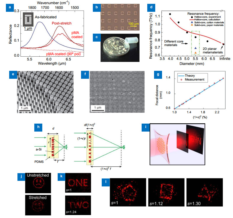
Extensive reports are on the tunability of the resonance frequency of the metasurfaces by altering the period of the unit cells by stretching the substrate230, 232-238. The FTIR reflection spectra for an array of resonators on PDMS with a coupling distance of 60 nm are shown in Fig. 14(a). The as-fabricated resonator array had a resonance frequency of 5.78 μm (blue) and it shifted to 6.27 μm (dark red) after 25% stretching parallel to the SRR arms. The red line indicates the response of the array after functionalizing with coated p-mercaptoaniline (pMA). The dotted line shows the cross-polarized measurement for the functionalized array230. As shown in Figs. 14(b) and 14(c), polyethylene naphthalate (PEN) is also used to design a variable three-dimensional terahertz metamaterial to achieve resonance tunability72. Figure 14(d) shows that the resonance frequency of the metamaterial is decreased as the diameter of the tube folded from the metamaterial is increased.
A highly tunable elastic dielectric metasurface lens using a-Si nano-posts as the resonator and PDMS substrate has been reported70. The SEM images of the metasurface before and after the PDMS spin coating are shown in Figs. 14(e) and 14(f), respectively. The dielectric metasurface is operating at 915 nm, with focal distance tuning from 600 μm to 1400 μm with a focusing efficiency above 50%. The measured and analytically predicted focal distances for different strain values versus the square of the stretch ratio are shown in Fig. 14(g). As illustrated in Fig. 14(h), by stretching the metasurface with a stretch ratio of (1+ε), scales its focal length by a factor of (1+ε)2, providing a large tunability. A tunable flat metasurface optical zoom lens on a stretchable PDMS substrate with gold plasmonic resonators has also been reported that the measured focal length could continuously change from 150 to 250 μm73.
Ultrathin metasurfaces and metadevices fabricated on the elastic substrate are flexible and tunable through mechanical deformation like stretching. Different transparent flexible materials have been used to design and fabricate flexible and tunable metasurfaces. Polydimethylsiloxane (PDMS) is the most commonly used substrate to make flexible and tunable metasurfaces.
A strain multiplexed metasurface hologram fabricated with gold nanorods on a stretchable PDMS substrate can generate three different holographic patterns by stretching up to 130%231. The schematic illustration of the metasurface is shown in Fig. 14(i). As the substrate is stretched, the holographic image moves away from the device and enlarges in size. The three different holographic patterns by stretching the hologram metasurface are shown in Figs. 14(j)-14(l).
![Figure 14. Flexible tunable metamaterials made on elastic substrates.]()
Flexible tunable metamaterials made on elastic substrates.
(a) FTIR reflection spectra for the metamaterial with a coupling distance of 60 nm are shown. The inset shows SEM image of the fabricated sample. Image of (b) 2D planar metamaterial and (c) 3D terahertz metamaterial tube at a diameter of 4.00 mm. (d) Resonance frequency shifts as a function of core diameter for the hollow- and solid-core (cotton and paper) metamaterials tubes. SEM image of (e) the nano-posts before spin coating the first PDMS layer and (f) the nano-posts embedded in the PDMS. (g) Measured and analytically predicted focal distances (i.e. (1+ε)2×f) for different strain values versus the square of the stretch ratio ((1+ε)2). (h) A side view schematic illustration of a dielectric metasurface microlens that by stretching with a stretch ratio of (1+ε), the focal distance changes by (1+ε)2. (i) Schematic illustration of the metasurface hologram on the PDMS substrate. (j) and (k) Experimentally measured hologram images at an image plane 200 μm from the metasurface for a device that is not stretched and stretched. (l) Experimentally captured hologram images at a distance of 340 μm from the metasurface when the device is unstretched, stretched 112%, and 130%. Figure reproduced from: (a) ref.230, American Chemical Society; (b–d) ref.72, John Wiley and Sons; (e–h) ref.70, John Wiley and Sons; (i–l) ref.231, American Chemical Society.Micro-nanoelectromechanical systems
![Figure 15. Reconfigurable metamaterials using M-NEMS.]()
Reconfigurable metamaterials using M-NEMS.
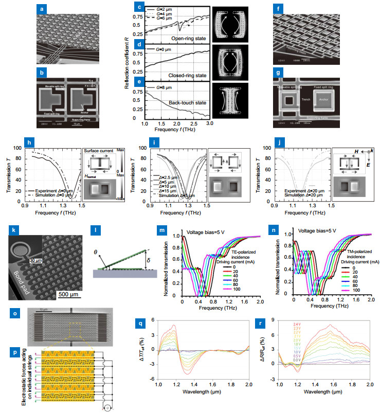
SEM image of (a) the metamaterial molecule array with micro-machined actuators and (b) the close-up top view of the unit cell. The measured reflection coefficient of the metamaterial under the TE polarized incidence in (c) the open-ring state (G=2 μm, 4 μm, and 6 μm), (d) the closed-ring state, and (e) the back-touch state (The simulation results of the induced surface currents by the magnetic response is shown on the right side of each figure). SEM image of (f) the metamaterial molecule array with micro-machined actuators and (g) the close-up top view of the unit cell. The simulated and measured transmission spectra for the TM polarization incident wave at (h) Δ =0, (i) Δ =2.5, 5, 10, 15 μm (from dark to light), and (j) Δ =20 μm. The simulated surface currents and normal magnetic field components are shown on the right side of each figure. (k) SEM image of the fabricated metamaterial (the zoom-in image of the omega-ring design is shown in the inset), (l) Cross-sectional view of released omega-ring showing the angle of curvature (θ) and bending height (δ). (m) and (n) Measured transmission spectra of Omega-ring metamaterial in the TE-polarized and TM-polarized incidence when the voltage bias is 5 V, respectively. (o) SEM image of the reconfigurable plasmonic metamaterial. (p) Schematic of the driving circuit (black) and a section of the metamaterial pattern consisting of a gold nanostructure (yellow) supported by silicon nitride strings (brown). (q) Transmission and (r) reflection spectra of the metamaterial for different static voltages. Figure reproduced from: (a–e) ref.76, John Wiley and Sons; (f–j) ref.74, John Wiley and Sons; (k–n) ref.77, AIP Publishing; (o–r) ref.48, Springer Nature.A switchable magnetic metamaterial is shown in Fig. 15(a)76. Each unit cell consists of two semi-square 0.5 μm thick aluminum split rings in which one of them is anchored on the substrate and the other one is movable by two identical electrostatic comb-drive actuators on both sides. Hence, the gap between the split rings can be tuned. Figure 15(b) shows how the movable ring could be moved away until it touches the back side of the fixed ring in the neighbor metamaterial unit cell. As shown in Figs. 15(c)-15(e), the reflection coefficient of the metamaterial is tuned as unit cell ring moves from open-ring state to back-touch state. Moreover, It was shown experimentally that the effective permeability (μ) can be changed from negative (-0.26) to positive (0.29) near the resonant frequency.
A reconfigurable metamaterial is shown in Fig. 15(f), with the wide tunability of resonant frequency by 31% for transverse electric polarization and 22% for transverse magnetic polarization74. Fig. 15(g) shows the unit cell consists of a pair of asymmetric split-ring resonators with one fixed to the substrate and the other on a movable frame. Three different configurations of the unit cell are obtained by adjusting the distance Δ between the rings. For example in TM mode, when Δ=0, as shown in Fig. 15(h), the rings touch each other from the front (face-touch state) and create a resonant frequency near 1.42 THz. As is shown in Fig. 15(i), by increasing Δ from 2.5 μm to 15 μm, the resonant frequency decreases from 1.32 THz to 1.22 THz. Finally as shown in Fig. 15(i), when Δ=20 μm, the ring touches the neighbor ring from the back (back-touch state). The resonant frequency becomes 1.16 THz. The strength of dipole-dipole coupling is tuned continuously by controlling the distance between the two rings.
Micro-nano-electromechanical systems (M-NEMS) are micro and nanometer scale components that integrate electrical and mechanical elements. These devices have the ability to sense, control, and actuate on the micro and nano-scale. They have been utilized to add tunability to a wide range of applications including RF switches in circuits, phase shifters, and antennas239-247, microphones, speakers, acoustic sensors, and accelerometers248-253, and recently in metamaterials and metasurfaces48, 74-83, 254-262.
Another approach is using a continuously tunable Omega-ring terahertz metamaterial as shown in Fig. 15(k), while each unit cell consists of an inner disk in the center and an omega-ring around it77. They have one layer of 500 nm thick Al on top and a 40 nm thick layer of Al2O3 on the bottom. The schematic side view of a reconfigurable omega-ring is shown in Fig. 15(l). When there is no current, the ring is released at an angle of θ due to residual stress in both layers. However, when a DC voltage is applied to the bias pads on two ends of the rings (bond pads), current flows through the Al metal lines and causes it to heat up. Since Al has a higher expanding rate than Al2O3, the ring will bend downwards. In TE mode, the resonance frequency of the unit cell decreases from 0.67 THz to 0.37 THz as current increases from 0 to 100 mA [shown in Fig. 15(m)]. In TM mode, the resonance frequency decreases from 0.73 THz to 0.43 THz as current increases from 0 to 100 mA [shown in Fig. 15(n)]. The similar approach is used by this group to design different types of tunable metasurfaces79, 82, 83, 262, 263.
An electromechanically reconfigurable plasmonic metamaterial operating in the near-infrared is shown in Fig. 15(o)48. The plasmonic metamolecules are formed on two pairs of parallel strings which have opposite voltage. Figure 15(p) shows how the distance between these pair of strings is controlled by the electrostatic force from a few volts of DC voltage. The positive (red) and negative (blue) charges are caused by the driving voltage U and create the pushing and pulling electrostatic forces (pink and green). Since their mass and dimensions are small, they can be driven synchronously to megahertz frequencies. The relative transmission and reflectance spectra of the metamaterial to a reference case where no voltage is applied are shown in Figs. 15(q) and 15(r), respectively. As can be seen, the transmission in the wavelength range of 1.1 μm to 1.3 μm shows around 5% modulation, and the reflectance is modulated up to 8% around a wavelength of 1.5 μm. Such reconfigurable metamaterials could provide continuous modulation of optical signals with megahertz bandwidth at microwatt power levels.
Conclusion
Although the field of metasurfaces have been introduced recently and designing new types of metasurfaces with novel applications to replace conventional optical elements is still in its early stages, the development of the active metasurfaces and metamaterials have already begun. This article gave an overview of the different types of tunable and reconfigurable metasurfaces and metamaterials through the active materials deployed. We have introduced transparent conductive oxides, ferroelectric materials, 2D materials, phase change materials, liquid crystals, semiconductors, and M-NEMS based on different tuning mechanisms such as electrical, thermal, optical, magnetic, and mechanical covering a wide span of operational frequency.
Different types of active materials and tuning mechanisms could be selected based on the device structure and application scenario. Lots of work in field of tunable metasurfaces has started and lots more need to be done like in large area low-cost fabrication, besides others. There are huge potentials for tunable metasurfaces and their progress will pave the way for realizing programmable flat optics for applications such as tunable optical lenses, dynamic holographic display and laser beam steering, etc., in the near future.
Other notable mechanisms used to design tunable metasurfaces and metadevices has been reported in a few articles. For example, electrical control of diodes has been used especially in lower frequency spectrums up to around 10 GHz265-274. Since the size of diodes limits the minimum size of each unit cell, it is not possible to design tunable metasurfaces for higher frequencies using diodes. Microfluidics is another technology used to design tunable metasurfaces from low frequency around 10 GHz275, 276 up to THz spectrum277-279. Magnesium is another tunable material that can undergo metal-to-dielectric phase-transition to form magnesium hydride (MgH2) by absorbing up to 7.6 wt % hydrogen280, which has been used in tunable metamaterials281-283. Last but not least, ferrites (magnet) materials are used specifically by coupling of the ferrite cuboid with Mie resonance of dielectric materials to magnetically tune the properties of different types of the metamaterials284-289.
Operation spectrum Modulation speed Tuning Mechanism Tuning range/depth Reference Transparent conductive oxides Visible 10 MHz Electrical 30% 47 172 kHz Electrical 15% 85 Ferroelectrics GHz to visible NA Electrical 19% 264 NA Thermal 43% 52 NA Optical 1.50% 61 Two dimensional (2D) materials THz to visible 100 kHz Electrical 47% 50 20 GHz Electrical 95% 88 40 MHz Electrical 60% 151 Phase change materials THz to visible 294 MHz Optical 16% 172 2.77 GHz Optical 42% 168 312 MHz Optical 46% 175 Liquid Crystals (LCs) GHz to visible NA Thermal 15% 103 NA Optical 18% 101 20 Hz Electrical 15% 200 Semiconductors THz to visible NA Electrical 79% 139 1.2 GHz Optical 46.70% 58 Elastic materials GHz to visible NA Mechanical 8% 233 NA Mechanical 50.60% 72 M-NEMS GHz to visible 1 kHz Electrical 7.50% 76 1 kHz Electrical 31% 74 1.5 kHz Electrical 87% 81 Different methods mentioned in this article are compared in Table 1. Ferroelectric materials are mainly used in the spectral range below and up to THz frequency because of their high tunability but might also find applications in the shorter wavelength range. Phase change materials show large changes in refractive index in the middle and near IR spectrum. Although liquid crystals are mainly used in the visible spectrum, they have enough change in dielectric constant to be used even in the THz and GHz spectra. In general, electrical control through bias voltage or current injection would have their advantages in terms of device control, operation, and integration, by which TCOs, semiconductors, 2D materials, LCs, and phase change materials, as well as M-NEMS, are all promising choices. Thermal control has been used to tune ferroelectrics, phase change materials, and liquid crystals in metasurfaces. Optical tuning enables fast and low power operation and has been used in almost all types of tunable materials, i.e. in phase change materials and LCs to tune local temperature and refractive index, while in TCOs and semiconductors to tune the carrier concentration. Mechanical control is used to stretch or deform the flexible metasurfaces made of elastic materials, which could apply to tunable holograms and wearable electronics. The magnetic field is mainly used in LCs to control the alignment of molecules. One grant challenge for tunable metasurfaces and metadevices is the ability to address individual metasurface element, especially in the visible range, which is currently done mostly using TCOs and ferroelectrics.
-
References
Shelby R A, Smith D R, Schultz S. Experimental verification of a negative index of refraction. Science 292, 77-79 (2001).
DOI: 10.1126/science.1058847Smith D R, Padilla W J, Vier D C, Nemat-Nasser S C, Schultz S. Composite medium with simultaneously negative permeability and permittivity. Phys Rev Lett 84, 4184-4187 (2000).
DOI: 10.1103/PhysRevLett.84.4184Schurig D, Mock J J, Justice B J, Cummer S A, Pendry J B et al. Metamaterial electromagnetic cloak at microwave frequencies. Science 314, 977-980 (2006).
DOI: 10.1126/science.1133628Landy N I, Sajuyigbe S, Mock J J, Smith D R, Padilla W J. Perfect metamaterial absorber. Phys Rev Lett 100, 207402 (2008).
DOI: 10.1103/PhysRevLett.100.207402Pendry J B, Schurig D, Smith D R. Controlling electromagnetic fields. Science 312, 1780-1782 (2006).
DOI: 10.1126/science.1125907Smith D R, Vier D C, Koschny T, Soukoulis C M. Electromagnetic parameter retrieval from inhomogeneous metamaterials. Phys Rev E 71, 036617 (2005).
DOI: 10.1103/PhysRevE.71.036617View full references list -
Author Information
-
Copyright
Open Access. © The Author(s). This article is licensed under a Creative Commons Attribution 4.0 International License. To view a copy of this license, visit http://creativecommons.org/licenses/by/4.0/. -
About this Article
Cite this Article
Arash Nemati, Qian Wang, Minghui Hong, et al. Tunable and reconfigurable metasurfaces and metadevices. Opto-Electronic Advances 1, 180009 (2018). DOI: 10.29026/oea.2018.180009Download CitationArticle History
- Received Date May 13, 2018
- Accepted Date June 20, 2018
- Available Online June 28, 2018
- Published Date June 28, 2018
Article Metrics
Article Views(54270) PDF Downloads(11182)
 OE Journals Group

Focuses on the advances of the cutting edge innovations of optics, photonics and optoelectronics
JCR Impact Factor: 22.4
CiteScore: 26.8
Open Access