E-mail Alert
 RSS
RSS-
Abstract
Inhomogeneity and low efficiency are two important factors that limit the application of laser-induced periodic surface structures (LIPSSs), especially on glass surfaces. In this study, two-beam interference (TBI) of femtosecond lasers was used to produce large-area straight LIPSSs on fused silica using cylindrical lenses. Compared with those produced using a single circular or cylindrical lens, the LIPSSs produced by TBI are much straighter and more regular. Depending on the laser fluence and scanning velocity, LIPSSs with grating-like or spaced LIPSSs are produced on the fused silica surface. Their structural colors are blue, green, and red, and only green and red, respectively. Grating-like LIPSS patterns oriented in different directions are obtained and exhibit bright and vivid colors, indicating potential applications in surface coloring and anti-counterfeiting logos.
Keywords
-
Introduction
In this study, we constructed an experimental setup for two-beam interference (TBI) of femtosecond lasers using a cylindrical lens, and efficiently produced large-area straight, regular LIPSSs on fused silica. The effects of the laser fluence and scanning velocity on the formation of the regular LIPSSs are studied in detail. Two types of LIPSSs, grating-like and spaced LSFLs, are produced on the fused silica surface. In addition, patterns of falling petals and two types of flowers with grating-like LIPSSs oriented in different directions are processed by mounting the fused silica on an x/y/z/⌀ four-axis translation stage. These patterns demonstrate bright pure colors when observed from different angles using a charge-coupled device (CCD).
Various methods have been developed to control the growth of LIPSSs in different materials. Jalil et al. obtained uniform periodic surface structures using two temporally delayed femtosecond laser beams30. Vass et al. demonstrated the two beam interferometric laser-induced backside wet etching (TWIN-LIBWE), and this mask-free procedure made it possible to fabricate grating in fused silica with a period substantially smaller than that previously reported31. Alamr et al. presented multi-scale periodic patterns with two-dimensional symmetry generated on stainless steel, polyimide and sapphire by combining direct laser interference patterning with the generation of LIPSSs in a one-step process32. Regular LIPSSs were obtained by chemical-etching assisted femtosecond laser ablation33-35. Large area uniform LIPSSs could be processed with cylindrical lenses36. Most studies have focused on the fabrication of regular LSFLs in conductors and semiconductors. However, few studies have been made on dielectrics, such as glass.
Efficient preparation of LIPSSs on glass surfaces has excellent potential for applications involving logos, color-based anti-counterfeiting, and wettability37, 38. However, efficient processing of regular LIPSSs on fused silica surfaces is rarely reported and remains a great challenge. Fused silica has a large band gap of 8.0 eV, much higher than normal glass such as silicate glass, bismuth glass, etc. Electron excitation under femtosecond laser irradiation is caused mainly by avalanche breakdown ionization, which forms a surface plasma layer39, 40. The laser fluences were usually very high (>1 J/cm2). Thereofore, the residual thermal effect on the surface after femtosecond laser ablation was very strong, leaving re-solidified layer of several μm thick41. Therefore, the LSFLs on fused silica were usually curved with many breaks and bifurcations7, 17.
Laser-induced periodic surface structures (LIPSSs) have been extensively studied in various materials, including conductors1-3, semiconductors3-5 and dielectrics6, 7, and exhibit a great potential applications in many fields such as structural colors8, 9, color-based anti-counterfeiting10, superhydrophobicity11, 12, and birefringence13-15. LIPSSs were classified into two types according to the relationship between the laser wavelength and LIPSS period: low-spatial-frequency LIPSSs (LSFLs), with a period close to the laser wavelength (λ–λ/2)16, 17, and high-spatial-frequency LIPSSs (HSFLs), with periods significantly smaller than the laser wavelength (<λ/2)18, 19. The formation of LSFLs have been studied for the last several decades. There are two main theoretical explanations for the formation of LSFLs. The first widely accepted theory attributed the generation of LSFLs to an interference between the electromagnetic field of the incident laser and a surface scattered wave generated by the laser on a rough surface20-22. The second theoretical explanation is the surface plasmon polarization (SPP) model. The surface is irradiated by laser pulses to produce micro-nano structures. Because these micro-nano structures scatter incident light, the spatially scattered light are formed to provide wave vectors missing from exciting SPP, and subsequent incident pulses can excite SPP, resulting in a periodic deposition of the laser energy and the formation of LSFLs23-25. The origin of HSFLs may be caused by the second harmonic generation (SHG)26, 27 or self-organization28, 29, and it is still under discussion.
Experimental
Schematic of the experimental set-up
The surface of the fused silica substrate is optically polished to a roughness of <0.5 nm. It is ultrasonically cleaned before and after ablation42. The surface micro-/nanostructures were observed by scanning electron microscope (SEM, S-4800 Cold-Field SEM, Hitachi).
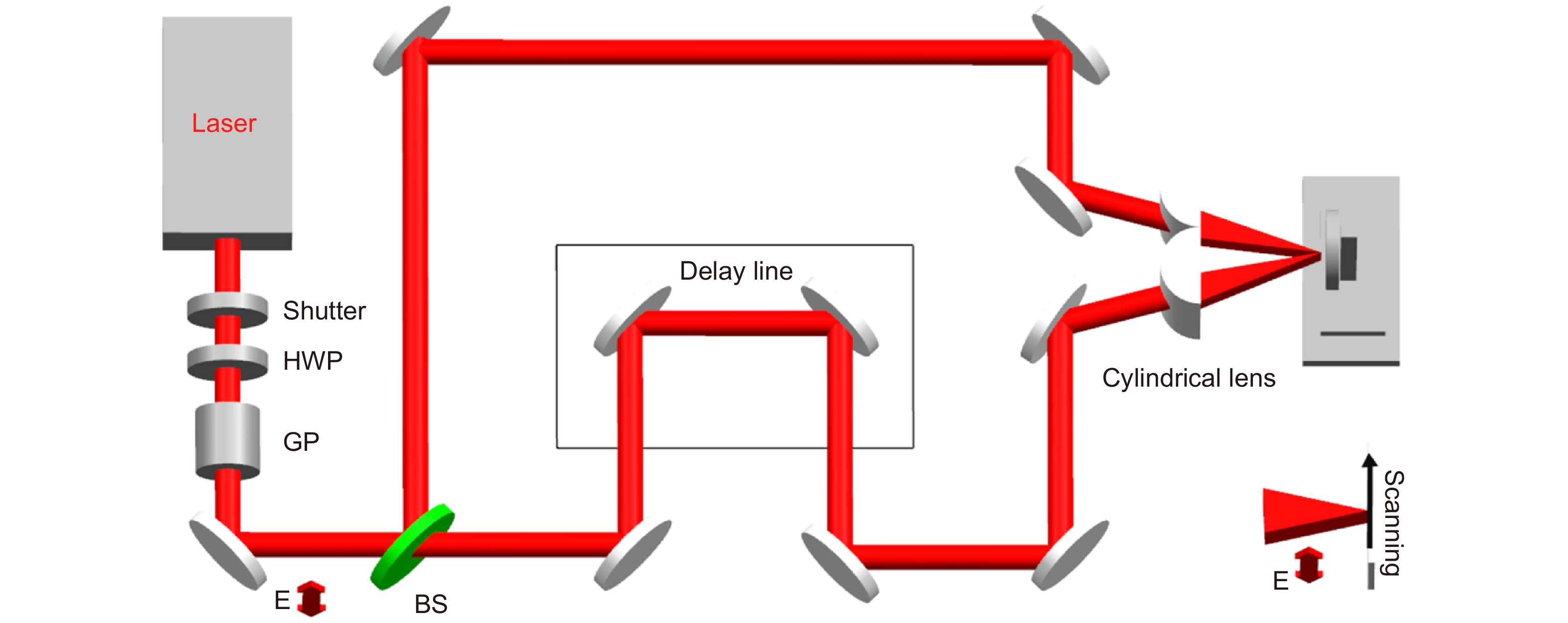
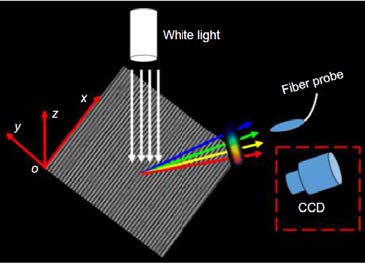
As shown in Fig. 1, the laser system is a commercial Ti:sapphire regenerative amplifier (Legend Elite, Coherent); it produces laser pulses at 800 nm, 50 fs, and 3 mJ with a repetition rate of 1–1000 Hz. The laser beam passes through a half-wave plate and Glan prism, which change the laser power and change the polarization to vertical. A mechanical shutter is used to control the laser irradiation time. The laser beam is split into two beams using a 50∶50 beam splitter, and the polarizations of the two beams are both vertical; one beam travels via a delay line and arrives at the sample surface at the same time as the other beam, where the zero point is determined by the double frequency signal of a BBO crystal. The fluence of a single beam is used to express the laser parameters. The angle 2θ between the laser beams is 9.3°, and the interference period Λ is calculated as 4.94 µm using the equation Λ = λ/2sinθ (laser wavelength λ = 0.8 µm). The two cylindrical lenses (focal length, 500 mm) are mounted vertically, and the focal spot is 50 µm wide and 2.0 mm long. The height of the two cylindrical lenses is at the same z position as well as the two foci, and the error is <0.1 mm. A fused silica substrate (MTI Group, China) is used as the sample and is mounted on an x/y/z/⌀ four-axis stage.
![Figure 1. Experimental setup for femtosecond laser interference using two cylindrical lenses. HWP: half-wave plate, GP: Glan prism, BS: beam splitter. The double arrow and letter E represent the laser polarization.]()
Experimental setup for femtosecond laser interference using two cylindrical lenses. HWP: half-wave plate, GP: Glan prism, BS: beam splitter. The double arrow and letter E represent the laser polarization.
The setup for the optical characterization
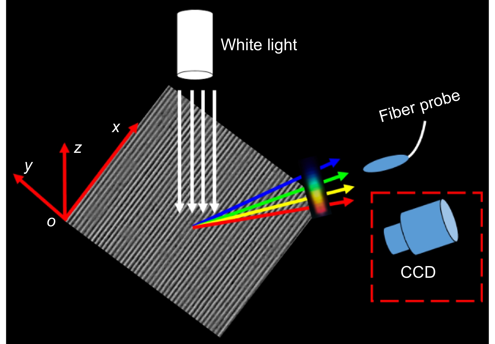
nλw=dsinα, ![Figure 2. Schematic of the setup for optical measurements.]()
Schematic of the setup for optical measurements.
To test the performance of the grating-like and spaced LIPSSs fabricated by the TBI, a wide-spectrum light source (400–2200 nm, tungsten halogen lamp) is perpendicularly illuminated on the sample surface. As is shown in Fig. 2, the diffraction spectra and the colors are measured by using a fiber spectrometer (USB2000+, Ocean Optics) and a charge-coupled device (CCD) at different angles. A fiber probe of the spectrometer (or CCD) moves in the y–z plane (perpendicular to the LIPSS direction). The optical resolution of the spectrometer is 1 nm. The angle between the fiber probe (or CCD) and the z axis is defined as the observation angle α. The diffraction equation reveal the relationship between diffraction spectra and observation angle α9:
where the integer n is the order of diffraction, λw is the wavelength of the diffraction spectrum measured at the angle α and d is the period of the LIPSSs (710 nm) or the interference stripes (4.94 μm).
Experimental results and discussion
LIPSSs on fused silica obtained by single beam and TBI
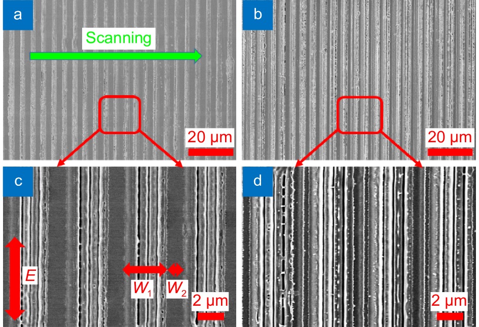
The measured interference period Λ is 4.94 μm, which is in good agreement with the theoretical value9, 44. As shown in Fig. 4(c), the interference period Λ consists of two components, namely, the width w1 of the ablation stripe and the width w2 of the unablated one (Λ = w1 + w2). The duty cycle of the ablation stripe is defined as w1/Λ and is approximately 75% at a scanning velocity of 8.2 mm/s, and the shifter between each two pulses is 8.2 μm. If the scanning velocity is decreased to 4.8 mm/s and the shifter between each two pulses is 4.8 μm, the duty cycle increases to 95%, which is similar to that of nanograting structures with the same period (718 nm), as shown in Fig. 4(d).
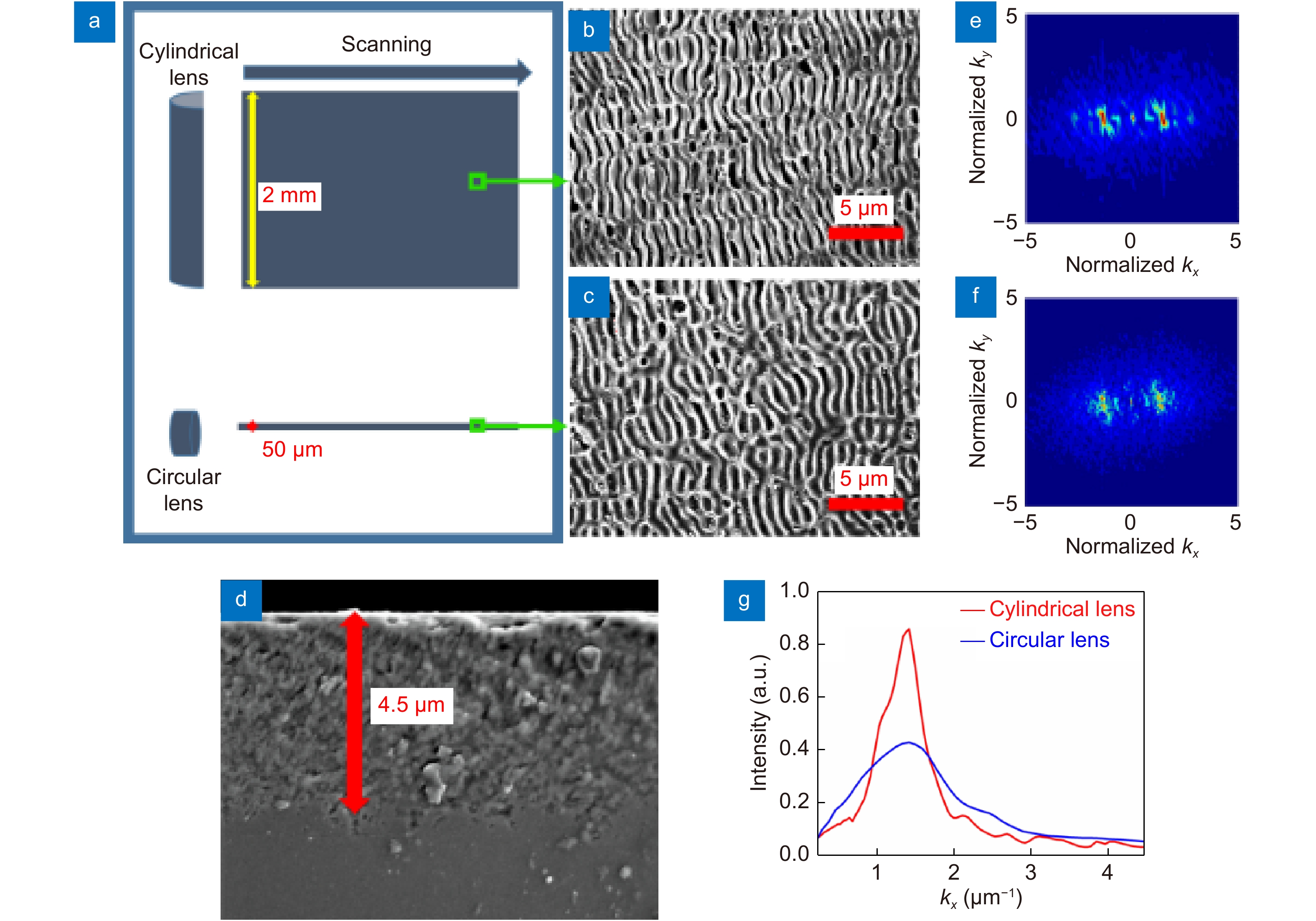
Figure 3(a) presents a schematic diagram of laser processing using a cylindrical lens or a circular lens; SEM images of the obtained LSFLs are shown in Figs. 3(b) and 3(c), respectively. The laser fluence is 2.8 J/cm2, the scanning velocity is 3.1 mm/s, and the accumulated pulses per spot is estimated to be 16. By these two processing methods, LSFLs with a period of 715 nm are induced on the fused silica surface. LSFL formation can be explained by the efficacy factor theory proposed by Sipe et al.21. The main mechanism is interference between the incident laser and the surface scattered light on the rough surface, which causes spatial energy modulation and uneven absorption inside the material, resulting in the appearance of LSFLs.
Figure 3(e) and 3(f) show the 2D Fourier transform (FT) images of the SEM images of Fig. 3(b) and 3(c), respectively. The peak of FT spectra by using a cylindrical lens is at 1.4±0.15 μm–1, which indicates that the LIPSS period is 715±75 nm. However, the peak of FT spectra by using a circular lens is at 1.4±0.3 μm–1, which indicates that the LIPSS period is 715±150 nm. When focusing a femtosecond laser with a cylindrical lens, the peak of FT spectra is higher and narrower. Therefore, those obtained using a cylindrical lens have a more regular arrangement than those obtained using a circular lens. The reason is that the scattered light travels mainly in the direction perpendicular to the focal line when a cylindrical lens is used; thus, the distribution of the interference field of the scattered light and the incident laser field is more regular.
![Figure 3. (a) Schematic diagram of laser processing of fused silica surface. Green squares indicate the regions at which the images in (b) and (c) were measured. SEM images of LSFLs obtained using (b) cylindrical lens and (c) circular lens. The laser fluence is 2.8 J/cm2, and the scanning velocity is 3.1 mm/s. The scale bar in (b) and (c) is 5 μm. (d) SEM image of cross section of LSFL on fused silica obtained using a laser focused by a cylindrical lens. (e) and (f) are the 2D-FT images of the LSFLs in (b) and (c), respectively. (g) is the FT spectra for ky = 0 μm–1.]()
(a) Schematic diagram of laser processing of fused silica surface. Green squares indicate the regions at which the images in (b) and (c) were measured. SEM images of LSFLs obtained using (b) cylindrical lens and (c) circular lens. The laser fluence is 2.8 J/cm2, and the scanning velocity is 3.1 mm/s. The scale bar in (b) and (c) is 5 μm. (d) SEM image of cross section of LSFL on fused silica obtained using a laser focused by a cylindrical lens. (e) and (f) are the 2D-FT images of the LSFLs in (b) and (c), respectively. (g) is the FT spectra for ky = 0 μm–1.
See Section 1 of Supplementary information, the schematic of the nanostructures on fused silica surface and the incident light in the numerical simulation with COMSOL multiphysics software (COMSOL 4.4.0.150) is presented45, 46. It explains well that the periodic structures generated by TBI are much more regular and straighter.
Note that fused silica has a large band gap of 8.0 eV. Electron excitation under femtosecond laser irradiation is caused mainly by avalanche breakdown ionization, which forms a surface plasma layer39, 40. As shown in Fig. 3(d), the residual thermal effect on the surface after femtosecond laser ablation of fused silica is very strong, and there is a 4.5-μm-thick re-solidified layer41. Therefore, the LSFLs obtained using a circular or cylindrical lens are distorted and exhibit many breaks and bifurcations.
![Figure 4. SEM images of micro-/nanostructures on fused silica produced by TBI, where each laser beam had a fluence of 2.8 J/cm2, and the scanning velocity was (a) 8.2 and (b) 4.8 mm/s. (c) and (d) are SEM images of the red areas in (a) and (b), respectively. The green arrow represents the scanning direction. The scale bar is 20 μm in (a) and (b), and is 2 μm in (c) and (d).]()
SEM images of micro-/nanostructures on fused silica produced by TBI, where each laser beam had a fluence of 2.8 J/cm2, and the scanning velocity was (a) 8.2 and (b) 4.8 mm/s. (c) and (d) are SEM images of the red areas in (a) and (b), respectively. The green arrow represents the scanning direction. The scale bar is 20 μm in (a) and (b), and is 2 μm in (c) and (d).
The periodic structures generated by TBI are much more regular and straighter. The reason is that TBI produces an interference pattern of ablation stripes, which are the excitation source for surface wave scattering during subsequent ablation by the femtosecond laser pulses. In contrast to that of structures produced using a single beam, the surface scattered waves excited by the interference pattern travel perpendicular to the interference stripe along the sample surface and constructively interfere with themselves. Therefore, the interference field of the surface scattered waves and the incident laser becomes more intense and more regular, forming very straight, uniform periodic structures on fused silica via periodic energy modulation. In addition, the interference pattern of the ablation stripes also constrains the growth of the LIPSSs, improving their regularity and straightness.
Figure 4 shows SEM images of the microstructures on fused silica obtained under different laser conditions. Figure 4(c) and 4(d) are SEM images of the red areas in Fig. 4(a) and 4(b), respectively. By combining with scanning, large-area straight, regular LSFLs with a period of 718 nm are produced on the ablation stripe of the TBI pattern. LSFLs are oriented parallel to the laser polarization. For semiconductors and metals, the surface plasmon polaritons (SPP) could easily be excited by the femtosecond laser, and LSFLs were perpendicular to the laser polarization direction4, 43. For the dielectrics such as fused silica, LSFLs were mainly caused by the interference of incident laser light with scattered light, and are parallel to the laser polarization7, 42.
Effect of laser fluence and scanning velocity on the formation of LIPSSs
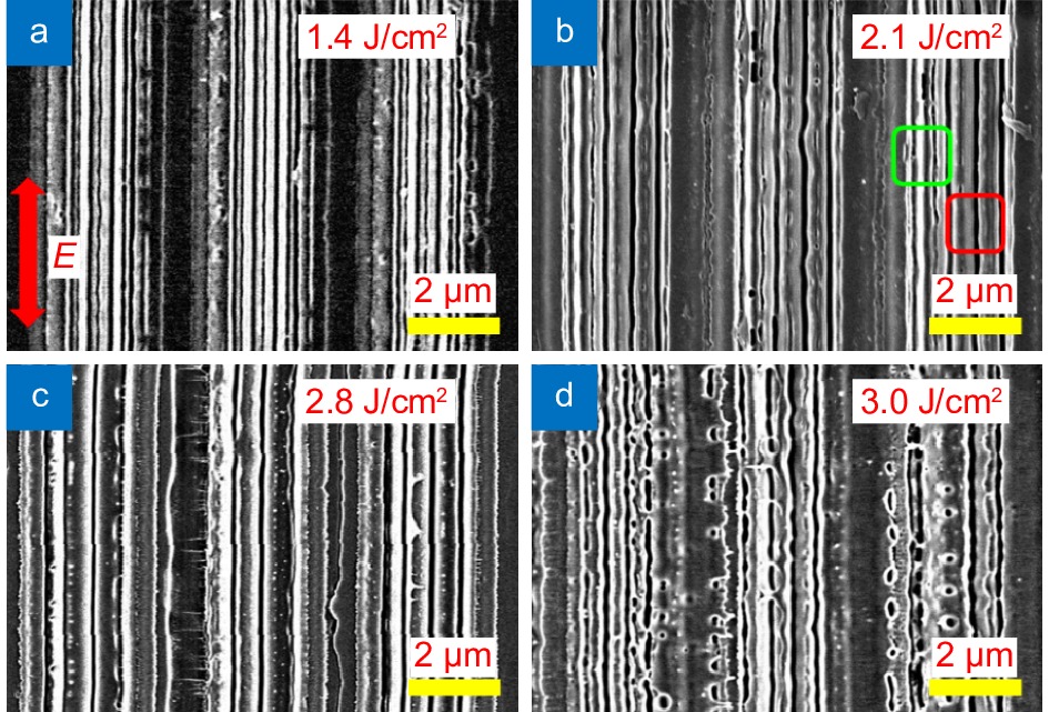
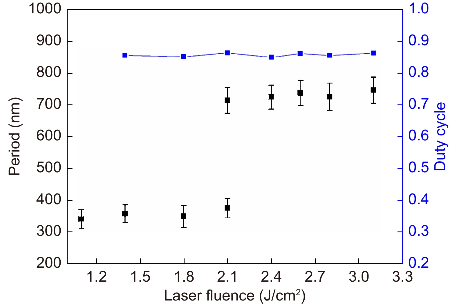
Figure 6 shows the LIPSS period and duty cycle for different fluences. The period and the error of the period in SEM are calculated by FFT (Fast Fourier Transform) analysis. HSFLs were formed at low fluences of 1.1–2.1 J/cm2, whereas LSFLs were formed at higher fluences of 2.1–3.1 J/cm2. At a fixed number of laser pulses (scanning velocity), a clear transition from HSFL to LSFL occurs when a critical fluence threshold (2.1 J/cm2) is exceeded7, 47. As shown in Fig. 5(c), at a laser fluence of 2.1 J/cm2, two periods exist simultaneously. The period in the red region is approximately 712 nm, whereas that in the green region is approximately 361 nm. The period of the HSFLs is approximately half that of the LSFLs. As the laser fluence decreases, the LSFLs split, and the period drops to half that of the original.
![Figure 5. SEM images of micro-/nanostructures on fused silica obtained at a scanning velocity of 6.2 mm/s and laser fluences of (a) 1.8, (b) 2.1, (c) 2.8, and (d) 3.2 J/cm2. The scale bar is 2 μm. Double arrow indicates the laser polarization direction.]()
SEM images of micro-/nanostructures on fused silica obtained at a scanning velocity of 6.2 mm/s and laser fluences of (a) 1.8, (b) 2.1, (c) 2.8, and (d) 3.2 J/cm2. The scale bar is 2 μm. Double arrow indicates the laser polarization direction.
To systematically study the production of regular LIPSSs by TBI, the effects of the laser fluence and scanning velocity are studied in detail. Figure 5 shows the surface micro-/nanostructures obtained at different fluences and a scanning velocity of 6.2 mm/s. At a laser fluence of 1.8 J/cm2, very straight and regular LIPSSs are formed on the ablation stripes, as shown in Fig. 5(a). These LIPSSs are parallel to the laser polarization direction. As the laser fluence is increased to 2.1 J/cm2, HSFLs and LSFLs are formed simultaneously on the ablation stripes. At 2.8 J/cm2, very straight and regular LSFLs are formed on the ablation stripes. At a laser fluence of 3.2 J/cm2, strong ablation occurs, and the LIPSSs become curved and exhibit deep ablation pits.
![Figure 6. LIPSS period and duty cycle versus fluence at a constant scanning velocity of 6.2 mm/s.]()
LIPSS period and duty cycle versus fluence at a constant scanning velocity of 6.2 mm/s.
![Figure 7. SEM images of micro-/nanostructures on fused silica obtained at a constant laser fluence of 2.8 J/cm2 and a scanning velocity of (a) 12, (b) 6.2, (c) 4.8, and (d) 2.4 mm/s. The scale bar is 5 μm. The double-headed arrow and E in (a) indicate the incident laser polarization direction.]()
SEM images of micro-/nanostructures on fused silica obtained at a constant laser fluence of 2.8 J/cm2 and a scanning velocity of (a) 12, (b) 6.2, (c) 4.8, and (d) 2.4 mm/s. The scale bar is 5 μm. The double-headed arrow and E in (a) indicate the incident laser polarization direction.
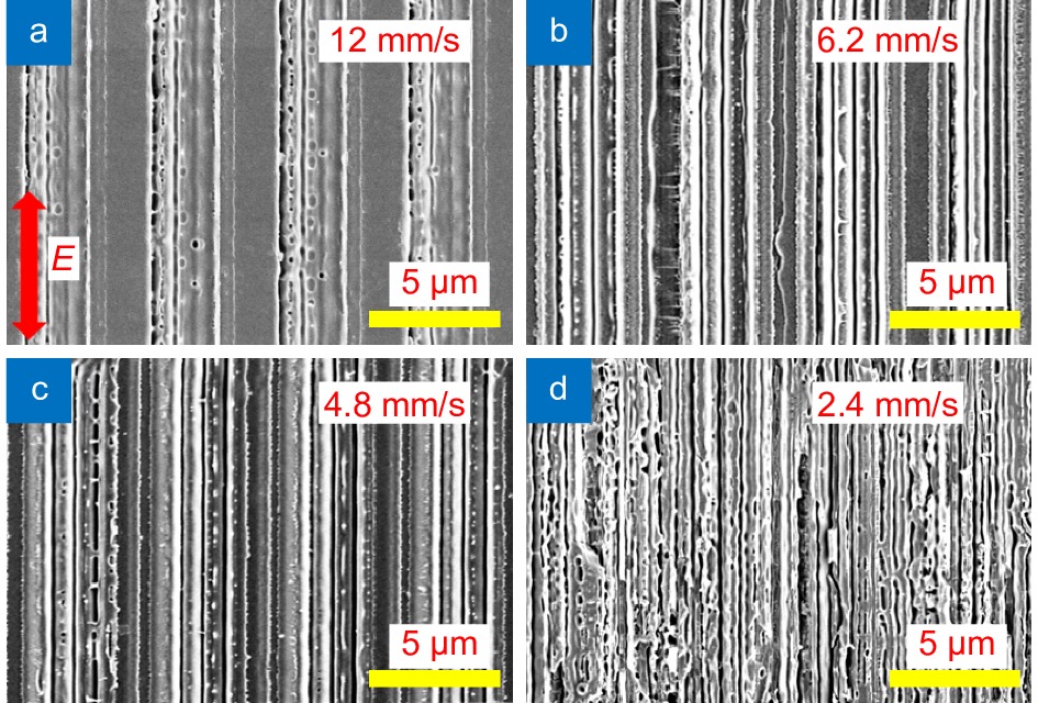
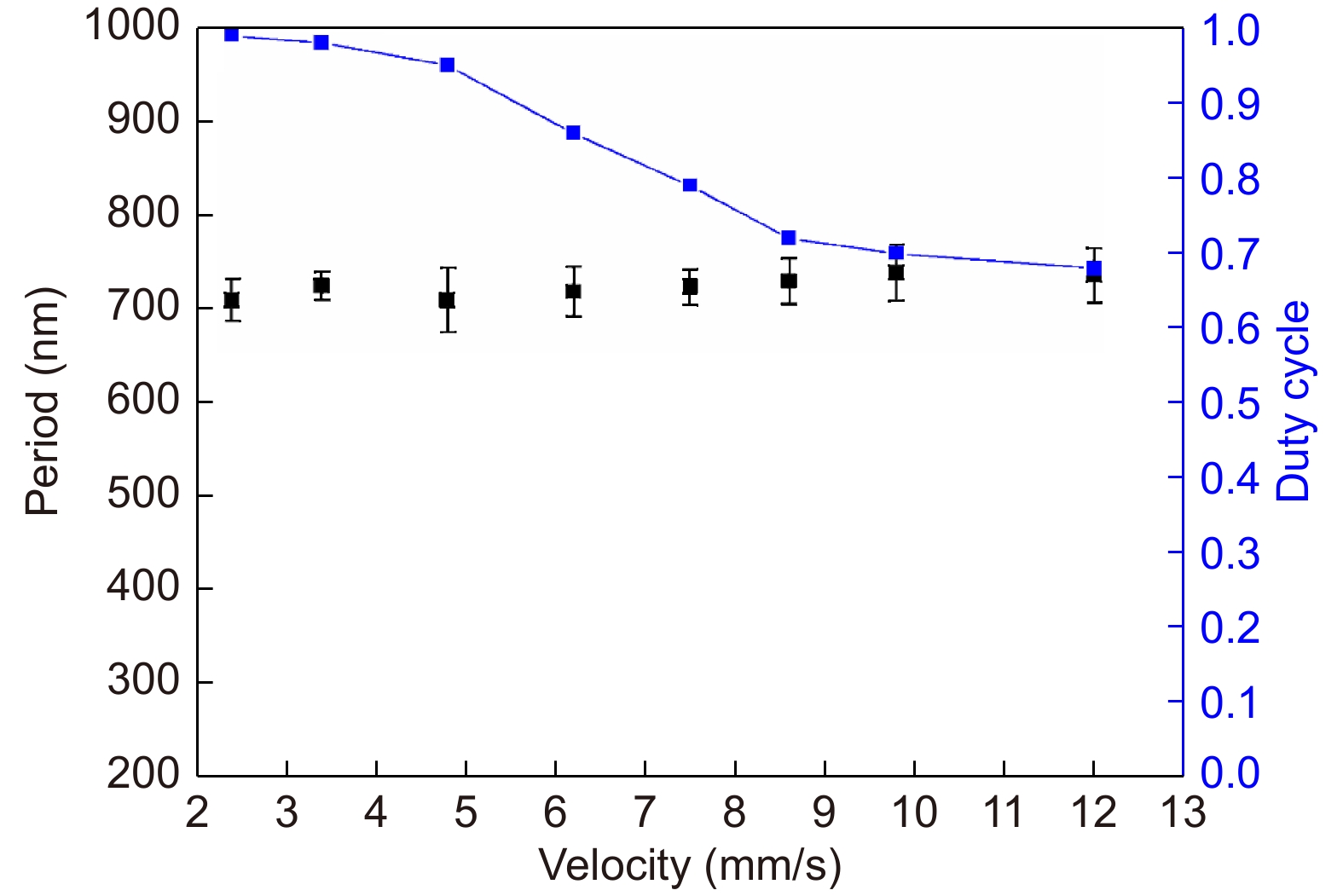
Figure 8 shows the LIPSS period and duty cycle for different scanning velocities at a constant laser fluence of 2.8 J/cm2. The period of the LIPSS fluctuates around 710 ± 15 nm with decreasing scanning velocity7, 42. In addition, the duty cycle of the ablation area increases slowly from 0.68 to 0.7 as the scanning velocity is from 12 to 8.8 mm/s. It increases quickly to 0.95 as the scanning velocity is decreased further to 4.8 mm/s. The unablated areas are barely visible, and the resulting structure consists of grating-like LIPSSs.
![Figure 8. LIPSS period and the duty cycle versus scanning velocity at a constant laser fluence of 2.8 J/cm2.]()
LIPSS period and the duty cycle versus scanning velocity at a constant laser fluence of 2.8 J/cm2.
The LIPSS period increases with increasing laser fluence; however, the duty cycle remains approximately 85% with only slight fluctuations. This is a very interesting observation, as it indicates that by varying the laser fluence within a certain range, regular LIPSSs can be obtained at a stable duty cycle. This finding has applications in structural color, anti-counterfeiting, and other applications.
Figure 7 shows SEM images of micro-/nanostructures on fused silica obtained at different scanning velocities and a constant laser fluence of 2.8 J/cm2. When the scanning velocity is as high as 12 mm/s, the averaged commulative pulses are only 4, and LIPSSs just begin to form. When the scanning velocity is decreased to 6.2 or 4.8 mm/s, very straight and regular LIPSSs are formed on the ablated area of the interference stripes. When the scanning velocity is decreased further to less than 3.0 mm/s, the averaged commulative pulses are more than 12. The silica surface is severely ablated and exhibits curved LIPSSs with considerable debris, as shown in Fig. 7(d).
Structural coloring
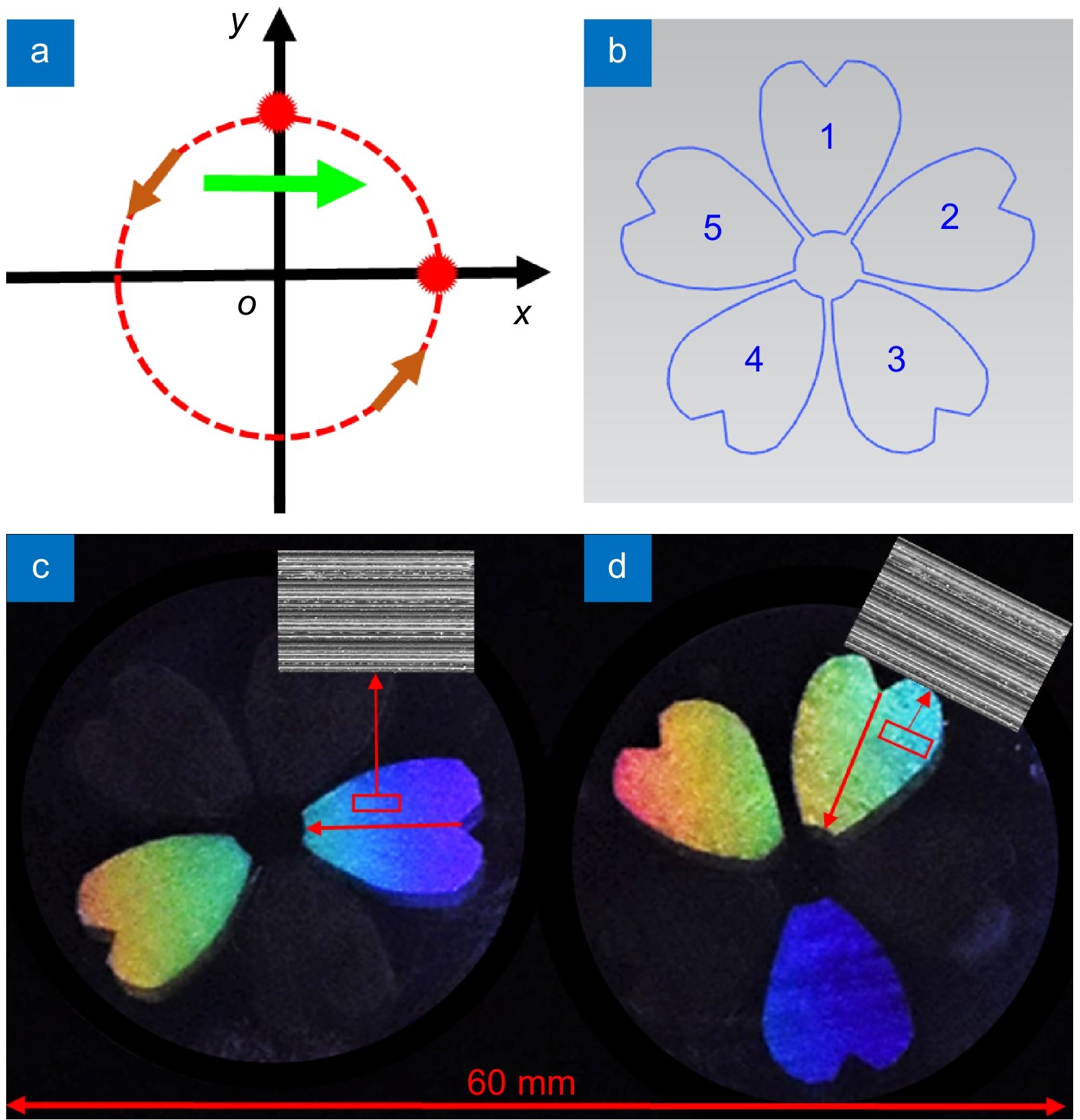
The flower pattern in tin foil is fabricated by 2D laser scanning, and covers on the fused silica. A schematic of the processing method is shown in Fig. 11(a), where the red spikes represent laser spots, O denotes the center of the rotatory stage, two short brown arrows on the circle represent the rotation direction, and the green arrow represents the scanning direction. Figure 11(b) shows the schematic of the flower pattern. By adjusting the azimuth of the laser focus relative to the center of the rotating table and scanning the sample horizontally, two different directional LIPSSs (the azimuth direction and the radial direction) can be created on the fused silica. Figure 11(c) and 11(d) show optical images of two flowers with five petals each. In Fig. 11(c), the grating-like LIPSSs forming each petal are oriented in the radial direction, whereas those in Fig. 11(d) are oriented in the azimuthal direction. Therefore, the colors of the two flowers differ greatly. However, each petal of the two flowers is bright and vivid.
![Figure 11. Colorful optical images of two flower patterns consisting of grating-like LIPSSs oriented in different directions. (a) Schematic of the processing method. The green arrow represents the scanning direction. (b) Schematic of the flower pattern. (c) The images of flowers with grating-like LIPSSs in radial direction, and (d) in azimuthal direction. Insets show SEM images of the grating-like LIPSSs in the open red squares.]()
Colorful optical images of two flower patterns consisting of grating-like LIPSSs oriented in different directions. (a) Schematic of the processing method. The green arrow represents the scanning direction. (b) Schematic of the flower pattern. (c) The images of flowers with grating-like LIPSSs in radial direction, and (d) in azimuthal direction. Insets show SEM images of the grating-like LIPSSs in the open red squares.
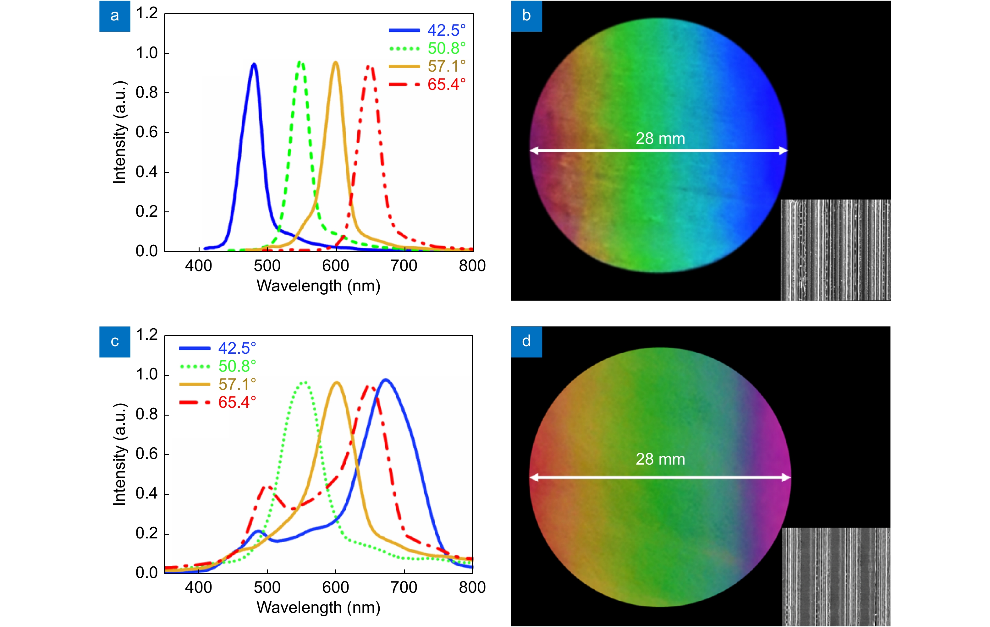
Figure 9(a) and 9(c) show the diffraction spectra of the grating-like LIPSSs (duty cycle of 95%) and spaced LIPSSs (duty cycle of 75%). The four diffraction spectra are observed at the four diffraction angles of 42.5°, 50.8°, 57.1° and 65.4°, respectively. The grating-like structures are fabricated by direct writing by TBI at a laser fluence of 2.8 J/cm² and a scanning velocity of 4.8 mm/s, and the space between the adjacent scanning lines is 0.5 mm. Fused silica with a diameter of 28 mm can be processed to obtain a colorful surface in 6 min. For the spaced LIPSSs, the laser fluence is 2.8 J/cm², and the scanning velocity is 8.2 mm/s.
The diffraction spectra of the sample with spaced LIPSSs exhibit two peaks when the sample is observed at a diffraction angle α of 42.5° in Fig. 9(c). The small peak at 480 nm is at nearly the same wavelength as the peak of the grating-like LIPSSs, and it is caused by the LIPSSs. The other peak is at 670 nm and is the fifth-order diffraction peak due to the interference stripes with a distance of 4.94 μm. The red peak is 5 times of the blue one, and the surface is fuchsia, as shown in Fig. 9(d). At a diffraction angle α of 50.8°, the diffraction peaks of the LIPSSs and interference stripes appear at 546 and 550 nm, respectively. The shifts in the two peaks are much smaller than the FWHM; thus, only one peak with a wider FWHM of 67 nm is observed, as shown in Fig. 9(c).
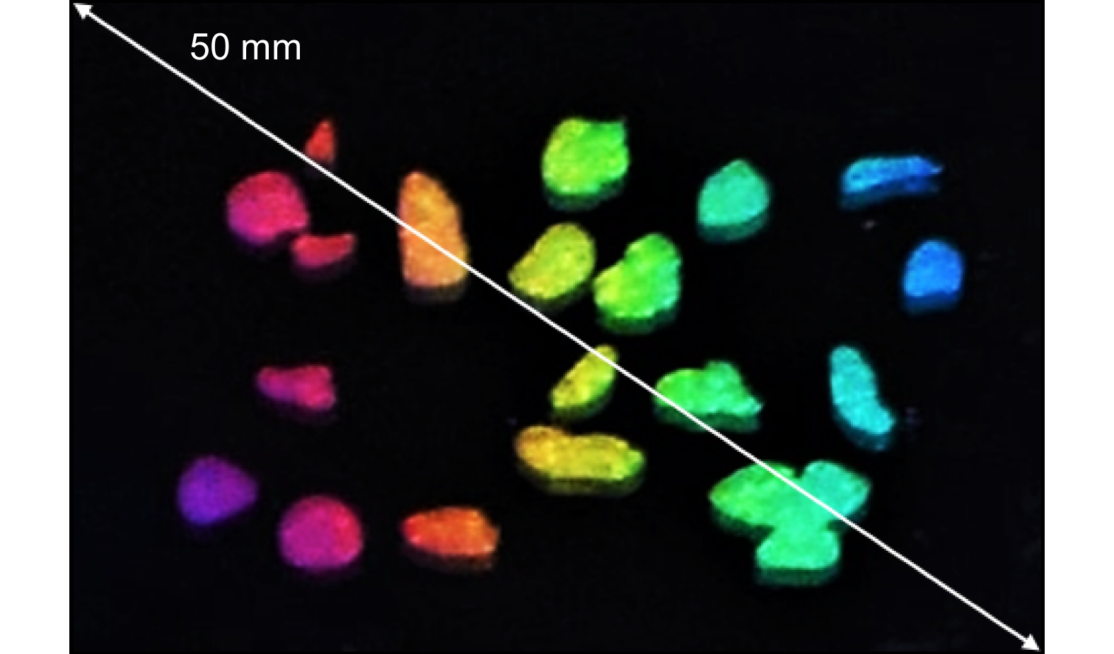
![Figure 10. Optical image of falling petal pattern consisting of grating-like LIPSSs.]()
Optical image of falling petal pattern consisting of grating-like LIPSSs.
Masks consisting of 1-mm-thick steel plates are fabricated by 2D laser scanning and placed on the fused silica. Grating-like LIPSSs are produced in a pattern of falling petals by direct writing by TBI. Figure 10 shows an optical image with excellent structural colors. All the petals (blue, green, red, and purple) are very vivid.
![Figure 9. Optical characterization of structured silica surface with grating-like LIPSSs and spaced LIPSSs. (a) Diffraction spectra and (b) color images of structured silica with grating-like LIPSSs. (c) Diffraction spectra and (d) color images of structured silica with spaced LIPSSs.]()
Optical characterization of structured silica surface with grating-like LIPSSs and spaced LIPSSs. (a) Diffraction spectra and (b) color images of structured silica with grating-like LIPSSs. (c) Diffraction spectra and (d) color images of structured silica with spaced LIPSSs.
The results shown in Fig. 9 are interesting for possible applications in anti-counterfeiting logos. The grating-like and spaced LIPSSs are produced on fused silica by simply changing the scanning velocity from 4.8 to 8.2 mm/s at a constant laser fluence of 2.8 J/cm². The surface with grating-like structure exhibits colors ranging from blue to red, whereas the color of the surface with spaced LIPSSs ranges from green to red, and the spectra have two diffraction peaks.
Figure 9(a) shows four diffraction spectra of the grating-like LIPSSs with peaks at 480, 550, 600, and 650 nm, where the full width at half-maximum (FWHM) is 33.4, 31.1, 35.8, and 36.8 nm, respectively. Each diffraction spectrum has only one peak, and the FWHM values are all less than 40 nm. Therefore, the optical images show a bright and vivid range of colors, as shown in Fig. 9(b).
Conclusions
This study demonstrated an efficient method of fabricating regular, straight large-area LIPSSs on fused silica through the interference of two femtosecond laser beams focused by cylindrical lenses. The effects of the laser fluence and scanning velocity on the formation of regular LIPSSs were studied in detail. Grating-like or spaced LIPSSs were produced on the fused silica surface and exhibited two types of structural color, specifically, blue, green, and red, or only green and red. Complex patterns with grating-like LIPSSs oriented in different directions were fabricated by mounting the fused silica on an x/y/z/⌀ four-axis translation stage. These patterns exhibited vivid structural colors when observed at different angles. The processing method proposed in this paper has potential applications for obtaining surface structural colors, anti-counterfeiting logos, superhydrophobicity, and so on.
Acknowledgements
We are grateful for financial supports from the Foundation of “Manufacturing beyond limits”, and the Science and Technology Commission of Shanghai Municipality (Grant No. 19ZR1414500), the National Natural Science Foundation of China (Grant Nos. 11474097, 11804227, 91950112), and the Open Fund of the State Key Laboratory of High Field Laser Physics (Shanghai Institute of Optics and Fine Mechanics).
-
References
[1] Livakas N, Skoulas E, Stratakis E. Omnidirectional iridescence via cylindrically-polarized femtosecond laser processing. Opto-Electron Adv 3, 190035 (2020).
DOI: 10.29026/oea.2020.190035[2] Graus P, Möller TB, Leiderer P, Boneberg J, Polushkin NI. Direct laser interference patterning of nonvolatile magnetic nanostructures in Fe60Al40 alloy via disorder-induced ferromagnetism. Opto-Electron Adv 3, 190027 (2020).
DOI: 10.29026/oea.2020.190027[3] Varlamova O, Hoefner K, Ratzke M, Reif J, Sarker D. Modification of surface properties of solids by femtosecond LIPSS writing: comparative studies on silicon and stainless steel. Appl Phys A 123, 725 (2017).
DOI: 10.1007/s00339-017-1362-y[4] Huang M, Zhao FL, Cheng Y, Xu NS, Xu ZZ. Origin of laser-induced near-subwavelength ripples: interference between surface plasmons and incident laser. ACS Nano 3, 4062–4070 (2009).
DOI: 10.1021/nn900654v[5] Zhang D S, Sugioka K. Hierarchical microstructures with high spatial frequency laser induced periodic surface structures possessing different orientations created by femtosecond laser ablation of silicon in liquids. Opto-Electron Adv 2, 190002 (2019).
DOI: 10.29026/oea.2019.190002[6] Shimotsuma Y, Sakakura M, Kazansky PG, Beresna M, Qiu JR et al. Ultrafast manipulation of self-assembled form birefringence in glass. Adv Mater 22, 4039–4043 (2010).
DOI: 10.1002/adma.201000921View full references list -
Author Information
-
Supplementary Information
-
Copyright
Open Access. © The Author(s). This article is licensed under a Creative Commons Attribution 4.0 International License. To view a copy of this license, visit http://creativecommons.org/licenses/by/4.0/. -
About this Article
Cite this Article
Long Chen, Kaiqiang Cao, Yanli Li, et al. Large-area straight, regular periodic surface structures produced on fused silica by the interference of two femtosecond laser beams through cylindrical lens. Opto-Electronic Advances 4, 200036 (2021). DOI: 10.29026/oea.2021.200036Download CitationArticle History
- Received Date August 10, 2020
- Accepted Date October 30, 2020
- Available Online December 24, 2021
- Published Date December 29, 2021
Article Metrics
Article Views(6938) PDF Downloads(1072)
 OE Journals Group

Focuses on the advances of the cutting edge innovations of optics, photonics and optoelectronics
JCR Impact Factor: 22.4
CiteScore: 26.8
Open Access