
 E-mail Alert
 RSS
RSS
| Citation: |
Lai SQ, Liu SB, Li ZL, Zhang ZN, Chen Z et al. Applications of lasers: A promising route toward low-cost fabrication of high-efficiency full-color micro-LED displays. Opto-Electron Sci 2, 230028 (2023). doi: 10.29026/oes.2023.230028

|
Applications of lasers: A promising route toward low-cost fabrication of high-efficiency full-color micro-LED displays
-
Abstract
Micro-light-emitting diodes (micro-LEDs) with outstanding performance are promising candidates for next-generation displays. To achieve the application of high-resolution displays such as meta-displays, virtual reality, and wearable electronics, the size of LEDs must be reduced to the micro-scale. Thus, traditional technology cannot meet the demand during the processing of micro-LEDs. Recently, lasers with short-duration pulses have attracted attention because of their unique advantages during micro-LED processing such as noncontact processing, adjustable energy and speed of the laser beam, no cutting force acting on the devices, high efficiency, and low cost. Herein, we review the techniques and principles of laser-based technologies for micro-LED displays, including chip dicing, geometry shaping, annealing, laser-assisted bonding, laser lift-off, defect detection, laser repair, mass transfer, and optimization of quantum dot color conversion films. Moreover, the future prospects and challenges of laser-based techniques for micro-LED displays are discussed.-
Keywords:
- laser /
- micro-LED /
- nano-processing /
- defective detection /
- laser repair /
- mass transfer /
- quantum dot
-

-
References
[1] Zhu SJ, Shan XY, Lin RZ, Qiu PJ, Wang Z et al. Characteristics of GaN-on-Si green micro-LED for wide color gamut display and high-speed visible light communication. ACS Photonics 10, 92–100 (2023). [2] Wu TZ, Sher CW, Lin Y, Lee CF, Liang SJ et al. Mini-LED and micro-LED: promising candidates for the next generation display technology. Appl Sci 8, 1557 (2018). doi: 10.3390/app8091557 [3] Qian YZ, Yang ZY, Huang YH, Lin KH, Wu ST. Directional high-efficiency nanowire LEDs with reduced angular color shift for AR and VR displays. Opto-Electron Sci 1, 220021 (2022). doi: 10.29026/oes.2022.220021 [4] Chen SWH, Shen CC, Wu TZ, Liao ZY, Chen LF et al. Full-color monolithic hybrid quantum dot nanoring micro light-emitting diodes with improved efficiency using atomic layer deposition and nonradiative resonant energy transfer. Photonics Res 7, 416–422 (2019). doi: 10.1364/PRJ.7.000416 [5] Xiong JH, Hsiang EL, He ZQ, Zhan T, Wu ST. Augmented reality and virtual reality displays: emerging technologies and future perspectives. Light Sci Appl 10, 216 (2021). doi: 10.1038/s41377-021-00658-8 [6] Hsiang EL, Yang ZY, Yang Q, Lai PC, Lin CL et al. AR/VR light engines: perspectives and challenges. Adv Opt Photonics 14, 783–861 (2022). doi: 10.1364/AOP.468066 [7] Chen Z, Yan SK, Danesh C. MicroLED technologies and applications: characteristics, fabrication, progress, and challenges. J Phys D Appl Phys 54, 123001 (2021). doi: 10.1088/1361-6463/abcfe4 [8] Lai SQ, Li QX, Long H, Ying LY, Zheng ZW et al. Theoretical study and optimization of the green InGaN/GaN multiple quantum wells with pre-layer. Superlattices Microstruct 155, 106906 (2021). doi: 10.1016/j.spmi.2021.106906 [9] Lin JY, Jiang HX. Development of microLED. Appl Phys Lett 116, 100502 (2020). doi: 10.1063/1.5145201 [10] Zhang FL, Su ZC, Li Z, Zhu Y, Gagrani N et al. High-speed multiwavelength InGaAs/InP quantum well nanowire array micro-LEDs for next generation optical communications. Opto-Electron Sci 2, 230003 (2023). doi: 10.29026/oes.2023.230003 [11] Lu TW, Lin XS, Guo QA, Tu CC, Liu SB et al. High-speed visible light communication based on micro-LED: A technology with wide applications in next generation communication. Opto-Electron Sci 1, 220020 (2022). doi: 10.29026/oes.2022.220020 [12] Yeh YW, Lin SH, Hsu TC, Lai SQ, Lee PT et al. Advanced atomic layer deposition technologies for micro-LEDs and VCSELs. Nanoscale Res Lett 16, 164 (2021). doi: 10.1186/s11671-021-03623-x [13] Chen SWH, Huang YM, Singh KJ, Hsu YC, Liou FJ et al. Full-color micro-LED display with high color stability using semipolar (20-21) InGaN LEDs and quantum-dot photoresist. Photonics Res 8, 630–636 (2020). doi: 10.1364/PRJ.388958 [14] Meng WQ, Xu FF, Yu ZH, Tao T, Shao LW et al. Three-dimensional monolithic micro-LED display driven by atomically thin transistor matrix. Nat Nanotechnol 16, 1231–1236 (2021). doi: 10.1038/s41565-021-00966-5 [15] Lee HE, Lee D, Lee TI, Shin JH, Choi GM et al. Wireless powered wearable micro light-emitting diodes. Nano Energy 55, 454–462 (2019). doi: 10.1016/j.nanoen.2018.11.017 [16] Yang X, Lin Y, Wu TZ, Yan ZJ, Chen Z et al. An overview on the principle of inkjet printing technique and its application in micro-display for augmented/virtual realities. Opto-Electron Adv 5, 210123 (2022). doi: 10.29026/oea.2022.210123 [17] Fan XT, Wu TZ, Liu B, Zhang R, Kuo HC et al. Recent developments of quantum dot based micro-LED based on non-radiative energy transfer mechanism. Opto-Electron Adv 4, 210022 (2021). doi: 10.29026/oea.2021.210022 [18] McCall SL, Levi AFJ, Slusher RE, Pearton SJ, Logan RA. Whispering-gallery mode microdisk lasers. Appl Phys Lett 60, 289–291 (1992). doi: 10.1063/1.106688 [19] Jin SX, Li J, Li JZ, Lin JY, Jiang HX. GaN microdisk light emitting diodes. Appl Phys Lett 76, 631–633 (2000). doi: 10.1063/1.125841 [20] Jin SX, Shakya J, Lin JY, Jiang HX. Size dependence of III-nitride microdisk light-emitting diode characteristics. Appl Phys Lett 78, 3532–3534 (2001). doi: 10.1063/1.1376152 [21] Jeon CW, Choi HW, Gu E, Dawson MD. High-density matrix-addressable AlInGaN-based 368-nm microarray light-emitting diodes. IEEE Photonics Technol Lett 16, 2421–2423 (2004). doi: 10.1109/LPT.2004.835626 [22] Liu ZJ, Chong WC, Wong KM, Lau KM. 360 PPI flip-chip mounted active matrix addressable light emitting diode on silicon (LEDoS) micro-displays. J Disp Technol 9, 678–682 (2013). doi: 10.1109/JDT.2013.2256107 [23] Chong WC, Cho WK, Liu ZJ, Wang CH, Lau KM. 1700 pixels per inch (PPI) passive-matrix micro-LED display powered by ASIC. In IEEE Compound Semiconductor Integrated Circuit Symposium 1–4 (IEEE, 2014);http://doi.org/10.1109/CSICS.2014.6978524. [24] Liu ZJ, Zhang K, Liu YB, Yan SW, Kwok HS et al. Fully multi-functional GaN-based micro-LEDs for 2500 PPI micro-displays, temperature sensing, light energy harvesting, and light detection. In IEEE International Electron Devices Meeting (IEDM) 38.1. 1–38.1. 4 (IEEE, 2018);http://doi.org/10.1109/IEDM.2018.8614692. [25] Tian PF, McKendry JJD, Gong Z, Zheng SL, Watson S et al. Characteristics and applications of micro-pixelated GaN-based light emitting diodes on Si substrates. J Appl Phys 115, 033112 (2014). doi: 10.1063/1.4862298 [26] Zhuang Z, Guo X, Liu B, Hu FR, Li Y et al. High color rendering index hybrid III-nitride/nanocrystals white light-emitting diodes. Adv Funct Mater 26, 36–43 (2016). doi: 10.1002/adfm.201502870 [27] Zhou YJ, Zhu X, Hu FC, Shi JY, Wang FM et al. Common-anode LED on a Si substrate for beyond 15 Gbit/s underwater visible light communication. Photonics Res 7, 1019–1029 (2019). doi: 10.1364/PRJ.7.001019 [28] Chen SWH, Huang YM, Chang YH, Lin Y, Liou FJ et al. High-bandwidth green semipolar (20–21) InGaN/GaN micro light-emitting diodes for visible light communication. ACS Photonics 7, 2228–2235 (2020). doi: 10.1021/acsphotonics.0c00764 [29] Wu TZ, Lin Y, Huang YM, Liu M, Singh KJ et al. Highly stable full-color display device with VLC application potential using semipolar μLEDs and all-inorganic encapsulated perovskite nanocrystal. Photonics Res 9, 2132–2143 (2021). doi: 10.1364/PRJ.431095 [30] Hassan NB, Dehkhoda F, Xie EY, Herrnsdorf J, Strain MJ et al. Ultrahigh frame rate digital light projector using chip-scale LED-on-CMOS technology. Photonics Res 10, 2434–2446 (2022). doi: 10.1364/PRJ.455574 [31] Zhu GQ, Liu YJ, Ming R, Shi F, Cheng MJ. Mass transfer, detection and repair technologies in micro-LED displays. Sci China Mater 65, 2128–2153 (2022). doi: 10.1007/s40843-022-2110-2 [32] Linghu CH, Zhang S, Wang CJ, Luo HY, Song JZ. Mass transfer for micro-LED display: transfer printing techniques. Semicond Semimetals 106, 253–280 (2021). [33] Tian WY, Wu YS, Wu TX, Dou L, Cao X et al. Mechanisms and performance analysis of GaN-based micro-LED grown on pattern sapphire substrate by laser lift-off Process. ECS J Solid State Sci Technol 11, 046001 (2022). doi: 10.1149/2162-8777/ac63e5 [34] Wei Q, Zhou F, Xu WZ, Ren FF, Zhou D et al. Demonstration of vertical GaN schottky barrier diode with robust electrothermal ruggedness and fast switching capability by eutectic bonding and laser lift-off techniques. IEEE J Electron Devices Soc 10, 1003–1008 (2022). doi: 10.1109/JEDS.2022.3222081 [35] Lu H, Guo WJ, Su CW, Li XL, Lu YJ et al. Optimization on adhesive stamp Mass-transfer of Micro-LEDs with support vector machine model. IEEE J Electron Devices Soc 8, 554–558 (2020). doi: 10.1109/JEDS.2020.2995710 [36] Chen FR, Bian J, Hu JL, Sun NN, Yang B et al. Mass transfer techniques for large-scale and high-density microLED arrays. Int J Extrem Manuf 4, 042005 (2022). doi: 10.1088/2631-7990/ac92ee [37] Leitão MF, Islim MS, Yin L, Viola S, Watson S et al. MicroLED-pumped perovskite quantum dot color converter for visible light communications. In IEEE Photonics Conference 69–70 (IEEE, 2017); http://doi.org/10.1109/IPCon.2017.8116011. [38] https://www.ledinside.cn/interview/20230515-55051.html. [39] https://www.ledinside.cn/news/20230601-55182.html. [40] https://m.ledinside.cn/news/20230505-54971.html. [41] Gu E, Jeon CW, Choi HW, Rice G, Dawson MD et al. Micromachining and dicing of sapphire, gallium nitride and micro LED devices with UV copper vapour laser. Thin Solid Films 453–454, 462–466 (2004). [42] Guo YN, Zhang Y, Yan JC, Chen X, Zhang S et al. Sapphire substrate sidewall shaping of deep ultraviolet light-emitting diodes by picosecond laser multiple scribing. Appl Phys Express 10, 062101 (2017). doi: 10.7567/APEX.10.062101 [43] Zheng BS, Ho CL, Cheng KY, Liao CL, Wu MC et al. Improved contact characteristics of laser-annealed p-GaN coated with Ni films. J Appl Phys 118, 085706 (2015). doi: 10.1063/1.4929522 [44] Park JB, Lee KH, Han SH, Chung TH, Kwak MK et al. Stable and efficient transfer-printing including repair using a GaN-based microscale light-emitting diode array for deformable displays. Sci Rep 9, 11551 (2019). doi: 10.1038/s41598-019-47449-1 [45] Haupt O, Brune J, Fatahilah M, Delmdahl R. MicroLEDs: high precision large scale UV laser lift-off and mass transfer processes. Proc SPIE 11989, 119890I (2022). [46] Yang X, Yan ZJ, Zhong CM, Jia H, Chen GL et al. Electrohydrodynamically printed high-resolution arrays based on stabilized CsPbBr3 quantum dot inks. Adv Funct Mater 11, 2202673 (2023). [47] Zhou XJ, Tian PF, Sher CW, Wu J, Liu HZ et al. Growth, transfer printing and colour conversion techniques towards full-colour micro-LED display. Prog Quantum Electron 71, 100263 (2020). doi: 10.1016/j.pquantelec.2020.100263 [48] Pan ZJ, Chen ZZ, Jiao F, Zhan JL, Chen YY et al. A review of key technologies for epitaxy and chip process of micro light-emitting diodes in display application. Acta Phys Sin 69, 198501 (2020). doi: 10.7498/aps.69.20200742 [49] Liu ZJ, Hyun BR, Sheng YJ, Lin CJ, Changhu M et al. Micro-light-emitting diodes based on InGaN materials with quantum dots. Adv Mater Technol 7, 2101189 (2022). doi: 10.1002/admt.202101189 [50] Choi M, Jang B, Lee W, Lee S, Kim TW et al. Stretchable active matrix inorganic light-emitting diode display enabled by overlay-aligned roll-transfer printing. Adv Funct Mater 27, 1606005 (2017). doi: 10.1002/adfm.201606005 [51] Charipar N, Auyeung RCY, Kim H, Charipar K, Piqué A. Hierarchical laser patterning of indium tin oxide thin films. Opt Mater Express 9, 3035–3045 (2019). doi: 10.1364/OME.9.003035 [52] Behrman K, Fouilloux J, Ireland T, Fern GR, Silver J et al. Early defect identification for micro light-emitting diode displays via photoluminescent and cathodoluminescent imaging. J Soc Inf Disp 29, 264–274 (2021). doi: 10.1002/jsid.985 [53] Shi SC, Bai WH, Lin CJ, Xuan TT, Dong GY et al. Uniformity and stability of quantum dot pixels evaluated by microscale fluorescence spectroscopy. Laser Photonics Rev 16, 2100699 (2022). doi: 10.1002/lpor.202100699 [54] Wang L, Pan ZX, Li B, Wang JJ, Guan XJ et al. Mechanism analysis of proton irradiation-induced increase of 3-dB bandwidth of GaN-based microlight-emitting diodes for space light communication. IEEE Trans Nucl Sci 67, 1360–1364 (2020). doi: 10.1109/TNS.2020.2964334 [55] Boussadi Y, Rochat N, Barnes JP, Bakir BB, Ferrandis P et al. Investigation of sidewall damage induced by reactive ion etching on AlGaInP MESA for micro-LED application. J Lumin 234, 117937 (2021). doi: 10.1016/j.jlumin.2021.117937 [56] Wong MS, Hwang D, Alhassan AI, Lee C, Ley R et al. High efficiency of III-nitride micro-light-emitting diodes by sidewall passivation using atomic layer deposition. Opt Express 26, 21324–21331 (2018). doi: 10.1364/OE.26.021324 [57] Mikulics M, Kordoš P, Gregušová D, Sofer Z, Winden A et al. Conditioning nano-LEDs in arrays by laser-micro-annealing: the key to their performance improvement. Appl Phys Lett 118, 043101 (2021). doi: 10.1063/5.0038070 [58] Wang H, Wang L, Sun J, Guo TL, Chen EG et al. Role of surface microstructure and shape on light extraction efficiency enhancement of GaN micro-LEDs: a numerical simulation study. Displays 73, 102172 (2022). doi: 10.1016/j.displa.2022.102172 [59] Lai SQ, Lin WS, Chen JL, Lu TW, Liu SB et al. The impacts of sidewall passivation via atomic layer deposition on GaN-based flip-chip blue mini-LEDs. J Phys D Appl Phys 55, 374001 (2022). doi: 10.1088/1361-6463/ac7b51 [60] Xu Y, Cui JW, Hu ZL, Gao X, Gao X et al. Pixel crosstalk in naked-eye micro-LED 3D display. Appl Opt 60, 5977–5983 (2021). doi: 10.1364/AO.429975 [61] Kim JH, Kim BC, Lim DW, Shin BC. Control of adhesion force for micro LED transfer using a magnetorheological elastomer. J Mech Sci Technol 33, 5321–5325 (2019). doi: 10.1007/s12206-019-1024-4 [62] Mei Y, Xie MC, Yang T, Hou X, Ou W et al. Improvement of the emission intensity of GaN-based micro-light emitting diodes by a suspended structure. ACS Photonics 9, 3967–3973 (2022). doi: 10.1021/acsphotonics.2c01366 [63] Wu YF, Ma JS, Su P, Zhang LJ, Xia BZ. Full-color realization of micro-LED displays. Nanomaterials 10, 2482 (2020). doi: 10.3390/nano10122482 [64] Lin CH, Kang CY, Verma A, Wu TZ, Pai YM et al. Ultrawide color gamut perovskite and CdSe/ZnS quantum-dots-based white light-emitting diode with high luminous efficiency. Nanomaterials 9, 1314 (2019). doi: 10.3390/nano9091314 [65] Cai YF, Bai J, Wang T. Review of a direct epitaxial approach to achieving micro-LEDs. Chin Phys B 32, 018508 (2023). doi: 10.1088/1674-1056/ac90b5 [66] Steffen B, Nursidik Y, Hendrik S, Yuliati H, Joan DP et al. Femtosecond laser lift-off with sub-bandgap excitation for production of free-standing GaN light-emitting diode chips. Adv Eng Mater 22, 1901192 (2019). doi: 10.1002/adem.201901192 [67] Fan SKS, Hsu CY, Jen CH, Chen KL, Juan LT. Defective wafer detection using a denoising autoencoder for semiconductor manufacturing processes. Adv Eng Inf 46, 101166 (2020). doi: 10.1016/j.aei.2020.101166 [68] Bi ZX, Chen Z, Danesh F, Samuelson L. From nanoLEDs to the realization of RGB-emitting microLEDs. Semicond Semimetals 106, 223–251 (2021). [69] Li XH, Kundaliya D, Tan ZJ, Anc M, Fang NX. Quantum dots color converters for microLEDs: material composite and patterning technology. In 2020 Conference on Lasers and Electro-Optics (CLEO) 1–2 (IEEE, 2020);http://doi.org/10.1364/CLEO_SI.2020.STu3P.7. [70] Lai SQ, Lu TW, Lin SH, Lin Y, Lin GC et al. Improved modulation bandwidth of blue Mini-LEDs by atomic-layer deposition sidewall passivation. IEEE Trans Electron Devices 69, 4936–4943 (2022). doi: 10.1109/TED.2022.3188738 [71] Wang L, Liu NY, Li B, Zhu HP, Shan XT et al. Comparison of X-ray and proton irradiation effects on the characteristics of InGaN/GaN multiple quantum wells light-emitting diodes. IEEE Trans Nucl Sci 67, 1345–1350 (2020). doi: 10.1109/TNS.2020.2975002 [72] Zhou R, Lin SD, Ding Y, Yang H, Ong YKK et al. Enhancement of laser ablation via interacting spatial double-pulse effect. Opto-Electron Adv 1, 180014 (2018). [73] Bellouard Y, Lehnert T, Clavel R, Sidler T, Gotthardt R. Laser annealing of shape memory alloys: a versatile tool for developing smart micro-devices. J Phys IV 11, Pr8-571–Pr8-576 (2001). [74] Dai YT, Xu G, Cui JL, Bai F. Laser microstructuring of sapphire wafer and fiber. Proc SPIE 7590, 75900O (2010). doi: 10.1117/12.841098 [75] Windemuth R. Plasma dicing for thin wafers. In European Microelectronics Packaging Conference (EMPC) 1–4 (IEEE, 2015). https://ieeexplore.ieee.org/document/7390697 [76] Li ZQ, Wang XF, Wang JL, Allegre O, Guo W et al. Stealth dicing of sapphire sheets with low surface roughness, zero kerf width, debris/crack-free and zero taper using a femtosecond Bessel beam. Opt Laser Technol 135, 106713 (2021). doi: 10.1016/j.optlastec.2020.106713 [77] Yadav A, Kbashi H, Kolpakov S, Gordon N, Zhou KM et al. Stealth dicing of sapphire wafers with near infra-red femtosecond pulses. Appl Phys A 123, 369 (2017). doi: 10.1007/s00339-017-0927-0 [78] Shah AP, Laskar MR, Rahman AA, Gokhale MR, Bhattacharya A. Inductively coupled plasma reactive ion etching of III-nitride semiconductors. AIP Conf Proc 1512, 494–495 (2013). [79] Chang KP, Lien PC, Yen CC, Chen PW, Horng RH et al. High performance AlGaInP-based micro-LED displays with novel pixel structures. IEEE Photonics Technol Lett 33, 1375–1378 (2021). doi: 10.1109/LPT.2021.3123447 [80] Zhang KX, Takahashi T, Ohori D, Cong GW, Endo K et al. High-quality nanodisk of InGaN/GaN MQWs fabricated by neutral-beam-etching and GaN regrowth: towards directional micro-LED in top-down structure. Semicond Sci Technol 35, 075001 (2020). doi: 10.1088/1361-6641/ab8539 [81] Fu WY, Hui KN, Wang XH, Wong K, Lai PT et al. Geometrical shaping of InGaN light-emitting diodes by laser micromachining. IEEE Photonics Technol Lett 21, 1078–1080 (2009). doi: 10.1109/LPT.2009.2022751 [82] Lin CM, Lin CF, Shieh BC, Yu TY, Chen SH et al. InGaN-Based Light-Emitting Diodes with a Sawtooth-shaped sidewall on sapphire substrate. IEEE Photonics Technol Lett 24, 1133–1135 (2012). doi: 10.1109/LPT.2012.2196511 [83] Lin CF, Lin CM, Chen KT, Huang WC, Lin MS et al. Blue light-emitting diodes with a roughened backside fabricated by wet etching. Appl Phys Lett 95, 201102 (2009). doi: 10.1063/1.3262968 [84] Li Y, Hong MH. Parallel laser micro/nano-processing for functional device fabrication. Laser Photonics Rev 14, 1900062 (2020). doi: 10.1002/lpor.201900062 [85] Voronenkov V, Bochkareva N, Gorbunov R, Zubrilov A, Kogotkov V et al. Laser slicing: a thin film lift-off method for GaN-on-GaN technology. Results Phys 13, 102233 (2019). doi: 10.1016/j.rinp.2019.102233 [86] Ludger O, Simon NG, Matthias S, Jan FD. On-the-fly bare die bonding based on laser induced forward transfer (LIFT). CIRP Annals 71, 41 (2022). doi: 10.1016/j.cirp.2022.03.042 [87] Wang FC, Liu Q, Xia JW, Huang MQ, Wang XF et al. Laser lift-off technologies for ultra-thin emerging electronics: mechanisms, applications, and progress. Adv Mater Technol 8, 2201186 (2023). doi: 10.1002/admt.202201186 [88] Gong YF, Gong Z. Laser-based micro/nano-processing techniques for microscale LEDs and full-color displays. Adv Mater Technol 8, 2200949 (2023). doi: 10.1002/admt.202200949 [89] Otto I, Mounir C, Nirschl A, Pfeuffer A, Schäpers T et al. Micro-pixel light emitting diodes: impact of the chip process on microscopic electro- and photoluminescence. Appl Phys Lett 106, 151108 (2015). doi: 10.1063/1.4918678 [90] Han SC, Xu CC, Li HJ, Liu SG, Xu HW et al. AlGaInP-based micro-LED array with enhanced optoelectrical properties. Opt Mater 114, 110860 (2021). doi: 10.1016/j.optmat.2021.110860 [91] Fu WY, Choi HW. Progress and prospects of III-nitride optoelectronic devices adopting lift-off processes. J Appl Phys 132, 060903 (2022). doi: 10.1063/5.0089750 [92] Sun WG, Ji LF, Lin ZY, Zheng JC, Wan ZY et al. Low-energy UV ultrafast laser controlled lift-off for high-quality flexible GaN-based device. Adv Funct Mater 32, 2111920 (2022). doi: 10.1002/adfm.202111920 [93] Kelly MK, Vaudo RP, Phanse VM, Görgens L, Ambacher O. Large Free-standing GaN substrates by hydride vapor phase epitaxy and laser-induced liftoff. Jpn J Appl Phys 38, L217–L219 (1999). doi: 10.1143/JJAP.38.L217 [94] Delmdahl R, Pätzel R, Brune J. Large-area laser-lift-off processing in microelectronics. Phys Procedia 41, 241–248 (2013). doi: 10.1016/j.phpro.2013.03.075 [95] Han HV, Lin HY, Lin CC, Chong WC, Li JR et al. Resonant-enhanced full-color emission of quantum-dot-based micro LED display technology. Opt Express 23, 32504–32515 (2015). doi: 10.1364/OE.23.032504 [96] Park S, Ko JH. Robust inspection of micro-LED chip defects using unsupervised anomaly detection. In International Conference on Information and Communication Technology Convergence (ICTC) 1841–1843 (IEEE, 2021);http://doi.org/10.1109/ICTC52510.2021.9620801. [97] Zhou RJ, Edwards C, Bryniarski CA, Popescu C, Goddard LL. 9nm node wafer defect inspection using three-dimensional scanning, a 405nm diode laser, and a broadband source. Proc SPIE 9424, 942416 (2015). [98] Kim K, Jung G, Kim J, Sung Y, Kang J et al. Correlation between photoluminescence and electroluminescence in GaN-related micro light emitting diodes: effects of leakage current, applied bias, incident light absorption and carrier escape. Opt Mater 120, 111448 (2021). doi: 10.1016/j.optmat.2021.111448 [99] Gui CQ, Ding XH, Zhou SJ, Gao YL, Liu XT et al. Nanoscale Ni/Au wire grids as transparent conductive electrodes in ultraviolet light-emitting diodes by laser direct writing. Opt Laser Technol 104, 112–117 (2018). doi: 10.1016/j.optlastec.2018.02.030 [100] Kuntoğlu M, Salur E, Canli E, Aslan A, Gupta MK et al. A state of the art on surface morphology of selective laser-melted metallic alloys. Int J Adv Manuf Technol 127, 1103–1142 (2023). doi: 10.1007/s00170-023-11534-7 [101] Zhang ZQ, Li DH, Li SC, Deng HL, Zhang SY et al. Effect of direct aging treatment on microstructure, mechanical and corrosion properties of a Si-Zr-Er modified Al-Zn-Mg-Cu alloy prepared by selective laser melting technology. Mater Charact 194, 112459 (2022). doi: 10.1016/j.matchar.2022.112459 [102] Gnanamuthu DS, Shankar VS. Laser heat treatment of iron-base alloys. Proc SPIE 527, 56–72 (1985). doi: 10.1117/12.946396 [103] Imam HZ, Al-Musaibeli H, Zheng YF, Martinez P, Ahmad R. Vision-based spatial damage localization method for autonomous robotic laser cladding repair processes. Robot Comput Integr Manuf 80, 102452 (2023). doi: 10.1016/j.rcim.2022.102452 [104] Taha K, Salah K, Yoo PD. Clustering the dominant defective patterns in semiconductor wafer maps. IEEE Trans Semicond Manuf 31, 156–165 (2018). doi: 10.1109/TSM.2017.2768323 [105] Bai HT, Tang H, Feng ZY, Liao ZS, Gao J et al. Development of a novel intelligent adjustable vision algorithm for LED chip repairing. IEEE Trans Ind Electron 69, 7109–7119 (2022). doi: 10.1109/TIE.2021.3095801 [106] Cok RS, Meitl M, Rotzoll R, Melnik G, Fecioru A et al. Inorganic light-emitting diode displays using micro-transfer printing. J Soc Inf Disp 25, 589–609 (2017). doi: 10.1002/jsid.610 [107] Choi KS, Joo J, Eom YS, Choi GM, Jang KS et al. Simultaneous transfer and bonding (SITRAB) process for Micro-LEDs using laser-assisted bonding with compression (LABC) process and SITRAB adhesive. In IEEE 71st Electronic Components and Technology Conference (ECTC) 1607–1613 (IEEE, 2021); http://doi.org/10.1109/ECTC32696.2021.00255. [108] Choi KS, Joo J, Choi GM, Yun HG, Moon SH et al. Laser-Assisted Bonding (LAB) Process and its bonding materials as technologies enabling the low-carbon era. In IEEE 72nd Electronic Components and Technology Conference (ECTC) 198–203 (IEEE, 2022);http://doi.org/10.1109/ECTC51906.2022.00042. [109] Lu XY, Zhu SJ, Lin RZ, Sun D, Cui XG et al. Performance improvement of red InGaN micro-LEDs by transfer printing from Si substrate onto glass substrate. IEEE Electron Device Lett 43, 1491–1494 (2022). doi: 10.1109/LED.2022.3189443 [110] Pan ZX, Guo C, Wang XC, Liu JC, Cao RM et al. Wafer-Scale Micro-LEDs Transferred onto an adhesive film for planar and flexible displays. Adv Mater Technol 5, 2000549 (2020). doi: 10.1002/admt.202000549 [111] Kim S, Jiang YJ, Towell KLT, Boutilier MSH, Nayakanti N et al. Soft nanocomposite electroadhesives for digital micro- and nanotransfer printing. Sci Adv 5, eaax4790 (2019). doi: 10.1126/sciadv.aax4790 [112] Trindade AJ, Guilhabert B, Xie EY, Ferreira R, Mckendry JJD et al. Heterogeneous integration of gallium nitride light-emitting diodes on diamond and silica by transfer printing. Opt Express 23, 9329–9338 (2015). doi: 10.1364/OE.23.009329 [113] Feinaeugle M, Gregorčič P, Heath DJ, Mills B, Eason RW. Time-resolved imaging of flyer dynamics for femtosecond laser-induced backward transfer of solid polymer thin films. Appl Surf Sci 396, 1231–1238 (2017). doi: 10.1016/j.apsusc.2016.11.120 [114] Zhang S, Luo HY, Wang SH, Chen Z, Nie S et al. A thermal actuated switchable dry adhesive with high reversibility for transfer printing. Int J Extrem Manuf 3, 035103 (2021). doi: 10.1088/2631-7990/abff69 [115] Marinov VR. Laser-enabled extremely-high rate technology for µLED assembly. SID Symp Dig Tech Pap 49, 692–695 (2018). [116] Prevatte C, Guven I, Ghosal K, Gomez D, Moore T et al. Pressure activated interconnection of micro transfer printed components. Appl Phys Lett 108, 203503 (2016). doi: 10.1063/1.4950992 [117] Ye N, Muliuk G, Zhang J, Abbasi A, Trindade AJ et al. Transfer print integration of waveguide-coupled germanium photodiodes onto passive silicon photonic ICs. J Lightwave Technol 36, 1249–1254 (2018). doi: 10.1109/JLT.2017.2777509 [118] Marinov VR, Swenson O, Atanasov Y, Schneck N. Laser-assisted ultrathin die packaging: insights from a process study. Microelectron Eng 101, 23–30 (2013). doi: 10.1016/j.mee.2012.08.016 [119] Kim S, Wu J, Carlson A, Jin SH, Kovalsky A et al. Microstructured elastomeric surfaces with reversible adhesion and examples of their use in deterministic assembly by transfer printing. Proc Natl Acad Sci USA 107, 17095–17100 (2010). doi: 10.1073/pnas.1005828107 [120] Bartlett MD, Crosby AJ. Material transfer controlled by elastomeric layer thickness. Mater Horiz 1, 507–512 (2014). doi: 10.1039/C4MH00106K [121] Tasoglu S, Yu CH, Gungordu HI, Guven S, Vural T et al. Guided and magnetic self-assembly of tunable magnetoceptive gels. Nat Commun 5, 4702 (2014). doi: 10.1038/ncomms5702 [122] Dendukuri D, Hatton TA, Doyle PS. Synthesis and self-assembly of amphiphilic polymeric microparticles. Langmuir 23, 4669–4674 (2007). doi: 10.1021/la062512i [123] Shin J, Kim H, Sundaram S, Jeong J, Park BI et al. Vertical full-colour micro-LEDs via 2D materials-based layer transfer. Nature 614, 81–87 (2023). doi: 10.1038/s41586-022-05612-1 [124] Kim J, Kim JH, Cho SH, Whang KH. Selective lift-off of GaN light-emitting diode from a sapphire substrate using 266-nm diode-pumped solid-state laser irradiation. Appl Phys A 122, 305 (2016). doi: 10.1007/s00339-016-9928-7 [125] Tang SKY, Derda R, Mazzeo AD, Whitesides GM. Reconfigurable self-assembly of mesoscale optical components at a liquid-liquid interface. Adv Mater 23, 2413–2418 (2011). doi: 10.1002/adma.201100067 [126] Hulteen JC, van Duyne RP. Nanosphere lithography: a materials general fabrication process for periodic particle array surfaces. J Vac Sci Technol 13, 1553–1558 (1995). doi: 10.1116/1.579726 [127] Kantrowitz A. Propulsion to orbit by ground-based lasers. Astronaut Aeronaut 10, 74–76 (1972). [128] Al-Attar HM, Mohammad MH, Alwan AH. Laser ablation of asphalt and coal in different solvents an in vitro study. Lasers Med Sci 38, 135 (2023). doi: 10.1007/s10103-023-03796-0 [129] Holmes AS. Laser processes for MEMS manufacture. Proc SPIE 4426, 203–209 (2002). doi: 10.1117/12.456807 [130] Li JW, Cao C, Qiu YW, Kuang CF, Liu X. Optical waveguides fabricated via femtosecond direct laser writing: processes, materials, and devices. Adv Mater Technol 8, 2300620 (2023). doi: 10.1002/admt.202300620 [131] Mathews SA, Auyeung RCY, Piqué A. Use of laser direct-write in microelectronics assembly. J Laser Micro/Nanoeng 2, 103–107 (2007). doi: 10.2961/jlmn.2007.01.0019 [132] Miller R, Marinov V, Swenson O, Chen ZG, Semler M. Noncontact selective laser-assisted placement of thinned semiconductor dice. IEEE Trans Compon Packaging Manuf Technol 2, 971–978 (2012). doi: 10.1109/TCPMT.2012.2183594 [133] Pique A, Charipar NA, Kim H, Auyeung RCY, Mathews SA. Applications of laser direct-write for embedding microelectronics. Advanced Laser Technologies 2006, 6606 (2007). doi: 10.1117/12.729635 [134] Goodfriend NT, Heng SY, Nerushev OA, Gromov AV, Bulgakov AV et al. Blister-based-laser-induced-forward-transfer: a non-contact, dry laser-based transfer method for nanomaterials. Nanotechnology 29, 385301 (2018). doi: 10.1088/1361-6528/aaceda [135] Eom YS, Choi GM, Jang KS, Joo J, Lee CM et al. Process window of simultaneous transfer and bonding materials using laser-assisted bonding for mini- and micro-LED display panel packaging. ETRI J (2023). DOI: 10.4218/etrij.2022-0471. [136] Karlitskaya NS, de Lange DF, Sanders R, Meijer J. Study of laser die release by Q-switched Nd: YAG laser pulses. Proc SPIE 5448, 935–943 (2004). doi: 10.1117/12.546674 [137] Saeidpourazar R, Li R, Li YH, Sangid MD, Lu CF et al. Laser-driven micro transfer placement of prefabricated microstructures. J Microelectromech Syst 21, 1049–1058 (2012). doi: 10.1109/JMEMS.2012.2203097 [138] Lee BG. Micro-droplet deposition by UV-pulsed laser induced forward transfer direct writing technology. Electron Mater Lett 8, 631–637 (2012). doi: 10.1007/s13391-012-2059-1 [139] He XN, Cheng JX, Li ZQ, Ye HT, Wei XF et al. Multimaterial three-dimensional printing of ultraviolet-curable ionic conductive elastomers with diverse polymers for multifunctional flexible electronics. ACS Appl Mater Interfaces 15, 3455–3466 (2023). doi: 10.1021/acsami.2c18954 [140] Li KH, Fu WY, Cheung YF, Wong KKY, Wang Y et al. Monolithically integrated InGaN/GaN light-emitting diodes, photodetectors, and waveguides on Si substrate. Optica 5, 564–569 (2018). doi: 10.1364/OPTICA.5.000564 [141] Fu WY, Choi HW. Development of chipscale InGaN RGB displays using strain-relaxed nanosphere-defined nanopillars. Nanotechnology 33, 285202 (2022). doi: 10.1088/1361-6528/ac6399 [142] Fu WY, Choi HW. Monolithic InGaN multicolor light-emitting devices. Phys Status Solidi-Rapid Res Lett 16, 2100628 (2022). doi: 10.1002/pssr.202100628 [143] Liu X, Li JJ, Zhang PP, Lu WT, Yang GL et al. Perovskite quantum dot microarrays: in situ fabrication via direct print photopolymerization. Nano Res 15, 7681–7687 (2022). doi: 10.1007/s12274-022-4466-4 [144] Lin Y, Fan XT, Yang X, Zheng X, Huang WZ et al. Remarkable black-phase robustness of CsPbI3 nanocrystals sealed in solid SiO2/AlOx sub-micron particles. Small 17, 2103510 (2021). doi: 10.1002/smll.202103510 [145] Lin Y, Zheng X, Shangguan ZB, Chen GL, Huang WZ et al. All-inorganic encapsulation for remarkably stable cesium lead halide perovskite nanocrystals: toward full-color display applications. J Mater Chem C 9, 12303–12313 (2021). doi: 10.1039/D1TC02685B [146] Zhang Y, Zhu HO, Zheng JL, Chai GY, Song ZP et al. Performance enhancement of all-inorganic perovskite quantum dots (CsPbX3) by UV-NIR laser irradiation. J Phys Chem C 123, 4502–4511 (2019). doi: 10.1021/acs.jpcc.8b11353 [147] Wei DZ, Wang CW, Wang HJ, Hu XP, Wei D et al. Publisher correction: experimental demonstration of a three-dimensional lithium niobate nonlinear photonic crystal. Nat Photonics 14, 709 (2020). doi: 10.1038/s41566-020-00698-3 [148] Tan DZ, Sharafudeen KN, Yue YZ, Qiu JR. Femtosecond laser induced phenomena in transparent solid materials: fundamentals and applications. Prog Mater Sci 76, 154–228 (2016). doi: 10.1016/j.pmatsci.2015.09.002 [149] Wang H, Wu Y, Ma MY, Dong S, Li Q et al. Pulsed laser deposition of CsPbBr3 films for application in perovskite solar cells. ACS Appl Energy Mater 2, 2305–2312 (2019). doi: 10.1021/acsaem.9b00130 [150] Jeon T, Jin HM, Lee SH, Lee JM, Park HI et al. Laser crystallization of organic–inorganic hybrid perovskite solar cells. ACS Nano 10, 7907–7914 (2016). doi: 10.1021/acsnano.6b03815 [151] Dos RR, Yang H, Ophus C, Ercius P, Bizarri G et al. Determination of the structural phase and octahedral rotation angle in halide perovskites. Appl Phys Lett 112, 071901 (2018). doi: 10.1063/1.5017537 [152] Chakraverty S, Ohtomo A, Kawasaki M. Controlled B-site ordering in Sr2CrReO6 double perovskite films by using pulsed laser interval deposition. Appl Phys Lett 97, 243107 (2010). doi: 10.1063/1.3525578 [153] Kim SJ, Byun J, Jeaon T, Jin HM, Hong HR et al. Perovskite Light-Emitting Diodes via Laser Crystallization: Systematic Investigation on Grain Size Effects for Device Performance. ACS Appl Mater Interfaces 10, 2490 (2018). doi: 10.1021/acsami.7b15470 [154] Chen XM, Wang ZX, Wu RJ, Cheng HL, Chui HC. Laser-induced thermal annealing of CH3NH3PbI3 perovskite microwires. Photonics 8, 30 (2021). doi: 10.3390/photonics8020030 [155] Chen J, Wu Y, Li XM, Cao F, Gu Y et al. Simple and fast patterning process by laser direct writing for perovskite quantum dots. Adv Mater Technol 2, 1700132 (2017). doi: 10.1002/admt.201700132 [156] Fenske M, Schultz C, Dagar J, Kosasih FU, Zeiser A et al. Improved electrical performance of perovskite photovoltaic mini-modules through controlled PbI2 formation using nanosecond laser pulses for P3 patterning. Energy Technol 9, 2000969 (2021). doi: 10.1002/ente.202000969 -
Access History

Figures(15)
Tables(3)
Article Metrics

Export File
Citation
Lai SQ, Liu SB, Li ZL, Zhang ZN, Chen Z et al. Applications of lasers: A promising route toward low-cost fabrication of high-efficiency full-color micro-LED displays. Opto-Electron Sci 2, 230028 (2023). doi: 10.29026/oes.2023.230028
Format
Content
 DownLoad:


-
Figure 1.
The corresponding developments of laser applications in the fabrication processes of micro-LED full-color displays: (a) Nano-processing, (b) Defective detection, (c) Laser repair and mass transfer, (d) Patterning and morphology modification for QD-CCF. Figure reproduced with permission from: (a) ref.51, Optical Society of America, under a Creative Commons Attribution License; (b) ref.44, 52, Springer Nature, under a Creative Commons Attribution License; (c, d) ref.53, John Wiley and Sons, under a Creative Commons Attribution License.
-
Figure 2.
(a–c) Schematic of LLO process. (d) Physical diagram of the LLO process.
-
Figure 3.
(a) Schematic of the femtosecond laser LLO technology machining setup. (b) The femtosecond laser LLO technology process, with single shots directed to the GaN surface for analysis of the beam characteristics shown on the left and the scanning pattern of the beam across the sapphire side in a uniform cross-pattern for lift-off experiments shown to the right. (c) Microscopic images of the wafer and chip surface after applying the two-step LLO process with increasing laser power. Figures reproduced with permission from: (a–c) ref.66, John Wiley and Sons, under a Creative Commons Attribution License.
-
Figure 4.
(a) PL intensity of good and defective chips detected by a micropulse laser. Inset: schematic illustrating adhesion is measured: after a 1.5 × 1.5 cm2 GaN piece on sapphire and a functional layer on a polyimide substrate are attached, the force generated by detaching these samples is measured. (b) Mapping image of the detected PL intensity after micropulse laser irradiation. (c) Optical microscopy image of defective chips on a real micro-LED wafer found using a PL intensity map. Figures reproduced with permission from: (a–c) ref.44, Springer Nature, under a Creative Commons Attribution License.
-
Figure 5.
(a) SEM images of pixel damaged by dry etching. (b) Electroluminescent images of the micro-LED array fabricated with 50 × 50 μm2 pixels and (c) sketch of the laser-based micro-LED repair method. Figures reproduced with permission from: (a, b) ref.52, (c) ref.88, John Wiley and Sons, under a Creative Commons Attribution License.
-
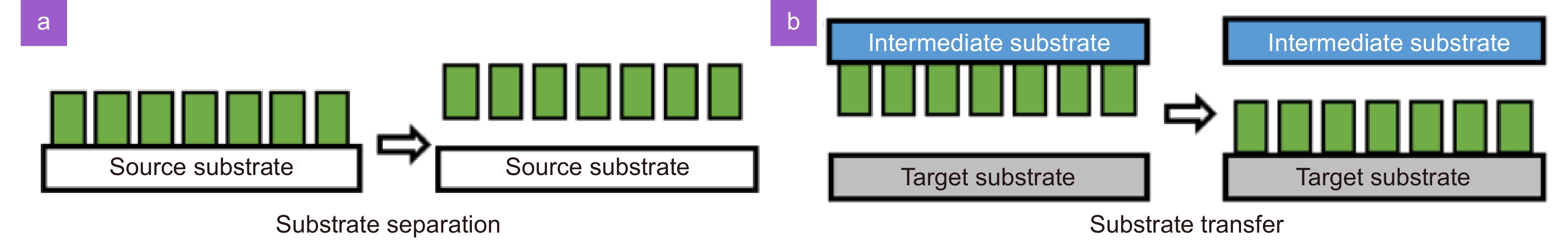
Figure 6.
Process of mass transfer for micro-LEDs.
-
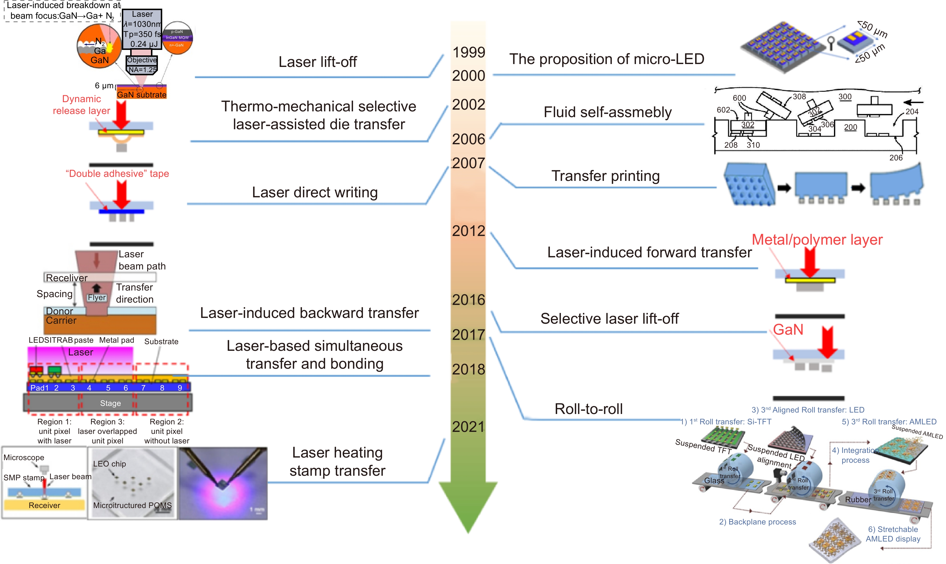
Figure 7.
Schematic of a brief chronology of the development of micro-LED displays and mass transfer techniques. Figures reproduced with permission from: ref.50, 85, 106,112, John Wiley and Sons, under a Creative Commons Attribution License; ref.85, Elsevier, under a Creative Commons Attribution License; ref.113, Optical Society of America, under a Creative Commons Attribution License; ref.114, IOP publishing, under a Creative Commons Attribution License.
-
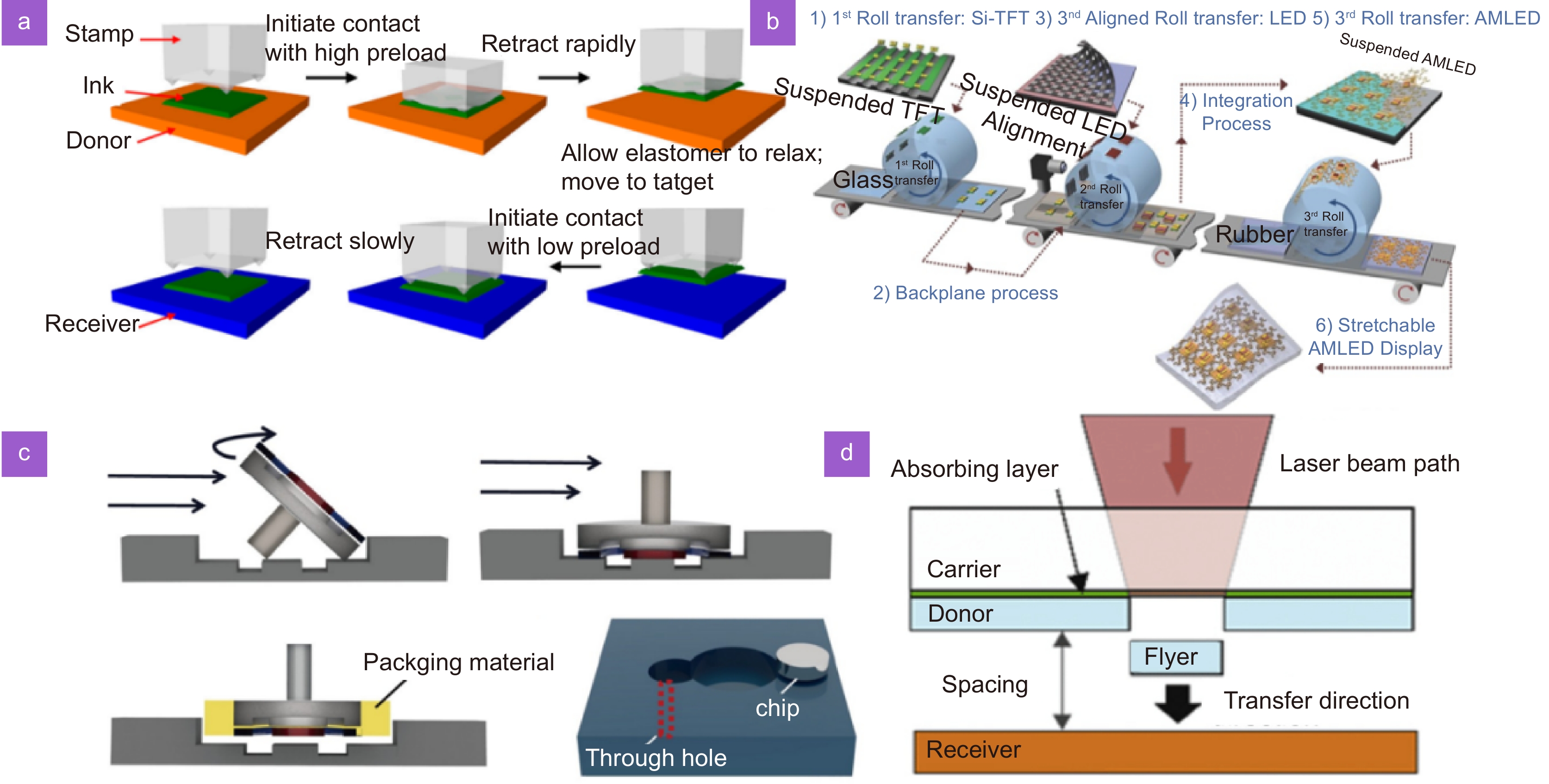
Figure 8.
The principles of mass transfer technologies for micro-LEDs. (a) Schematic illustration of a pick-and-place procedure via a stamp. (b) Schematic of the Roll-to-roll contact micro transfer printing (µTP) process. (c) An example of the specially designed micro-LED in a fluid self-assembly process. The navigation keel structure of LED chips ensures that the chips fall into the wells with the correct orientation aligned by torque forces. (d) Schematic of the laser-induced forward transfer process. Figures reproduced with permission from: (a) ref.119, Royal Society of Chemistry, under a Creative Commons Attribution License; (b) ref.31, Springer Nature, under a Creative Commons Attribution License; (c) ref.50, John Wiley and Sons, under a Creative Commons Attribution License; (d) ref.113, Elsevier, under a Creative Commons Attribution License.
-
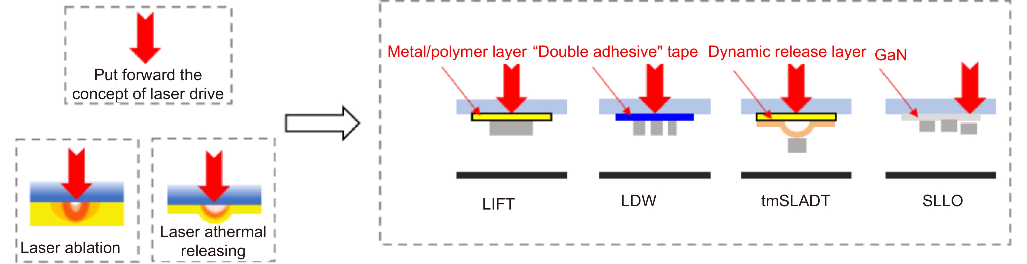
Figure 9.
Schematic of the principles of LIFT, LDW, tmSLADT and SLLO mass-transfer technologies.
-
Figure 10.
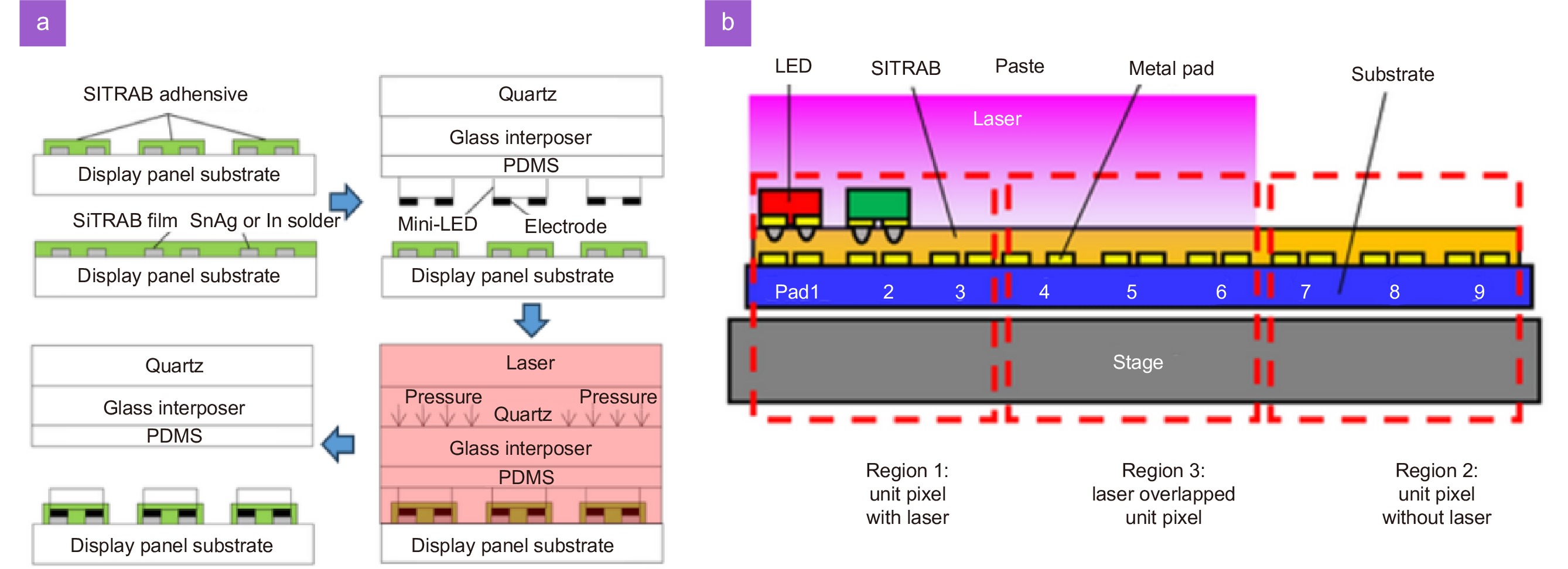
(a) Process flow of laser-based SITRAB and (b) tiling SITRAB process. Figures reproduced with permission from ref.135, John Wiley and Sons, under a Creative Commons Attribution License.
-
Figure 11.
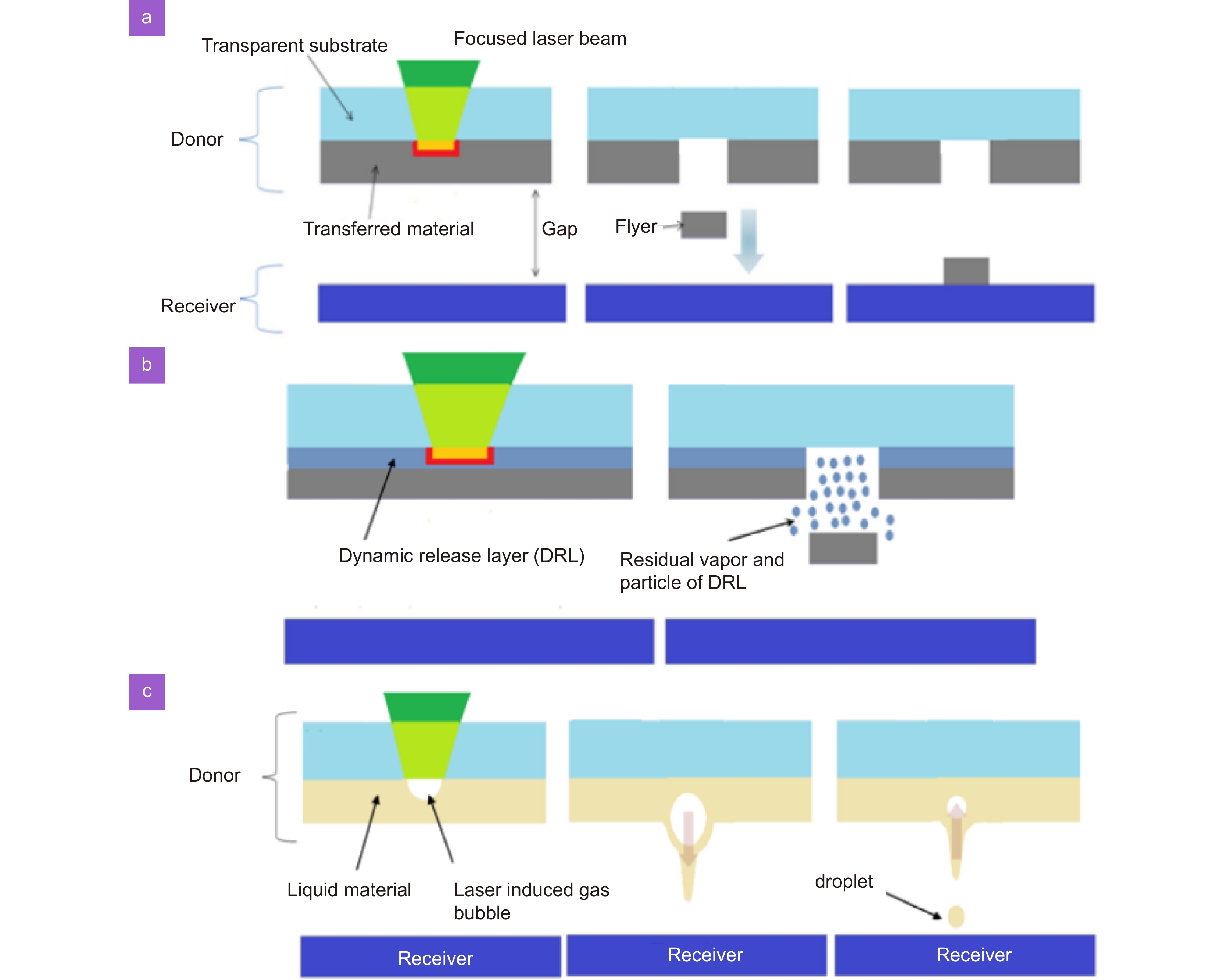
Sketch of the laser ablation-based LEAP mass transfer processes. (a) The LIFT process with the “donor” consists of a transparent substrate coated with a thin metal layer to be printed. A focused laser pulse is absorbed in the metal layer leading to local heating, and the resulting pressure at the interface provides the conditions for the transfer of the “flyer” part of the layer material. Finally, the transferred pixel land on the receiver. (b) tmSLADT with a DRL: the explosion of the DRL provides the driving force of the material transfer. (c) Schematic of LIFT of fluids: the laser pulse evaporates the solvent, which forms a gas bubble whose radius increases until its pressure equals the ambient pressure. Finally, the bubble collapses and a droplet separates from the jet filament.
-
Figure 12.
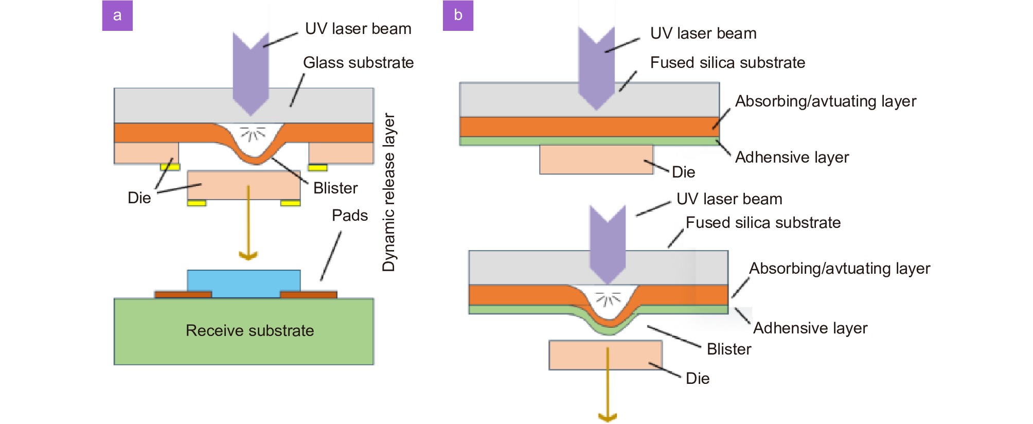
Schematic of laser-induced backward transfer with (a) unstructured carrier during LIBT and (b) structured carrier after transfer. Figures reproduced with permission from: (a-b) Ref.110, , Elsevier, under a Creative Commons Attribution License.
-
Figure 13.
(a) Schematic diagram of laser thermal releasing. (b) Double-layer dynamic release layer structure. Figures reproduced with permission from: (a) Ref.115, John Wiley and Sons, under a Creative Commons Attribution License.
-
Figure 14.
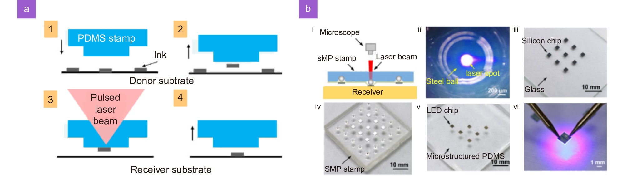
(a) Schematic of laser driven micro transfer placement technology. (b) Schematic of i) programmable transfer printing platform; ii) microscopic photography of the steel ball selectively heated by the laser beam; iii–v) programmable transfer printing of silicon chips to a microstructured PDMS substrate; vi) the printed LED chip is lighted by a multimeter. Figure reproduced with permission from ref.114, John Wiley and Sons, under a Creative Commons Attribution License.
-
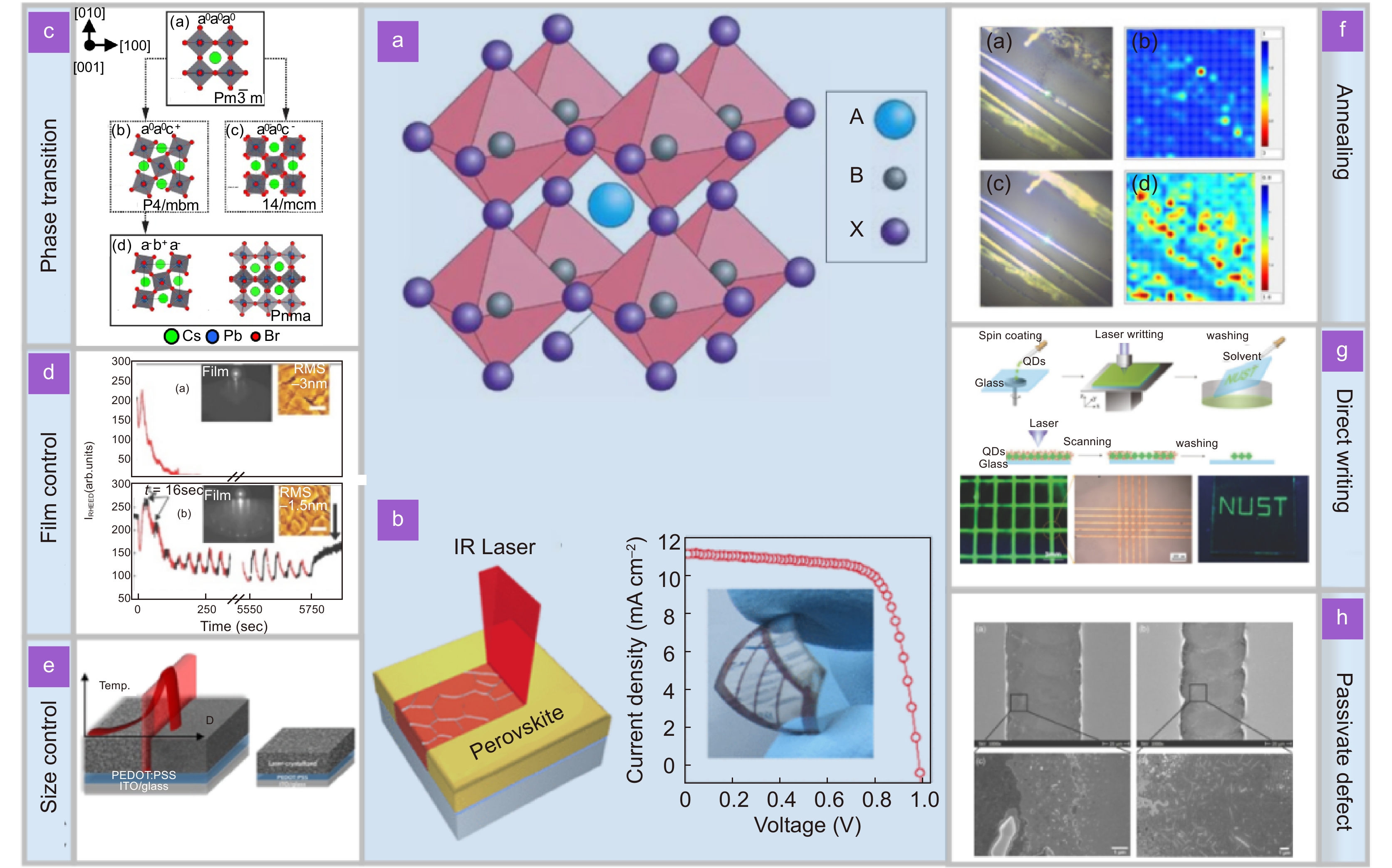
Figure 15.
(a) Structure of ABX3 lead halide perovskite. (b) Laser equipment of lead halide perovskite. (c) Laser causes perovskite phase transition. (d) Laser irradiation controls the film. (e) Laser irradiation changes the grain size of perovskite. (f) Laser annealing. (g) Laser direct writing process and patterning example. (h) Laser irradiation passivate perovskite defects. Figure reproduced with permission from: (b) ref.150, American Chemical Society, under a Creative Commons Attribution License; (c) ref.151, AIP Publishing, under a Creative Commons Attribution License; (d) ref.152, AIP Publishing, under a Creative Commons Attribution License; (e) ref.153, , American Chemical Society, under a Creative Commons Attribution License; (f) ref.154, MDPI Publishing, under a Creative Commons Attribution License; (g) ref.155, John Wiley and Sons, under a Creative Commons Attribution License; (h) ref.156, American Chemical Society, under a Creative Commons Attribution License.


