
 E-mail Alert
 RSS
RSS
| Citation: |
Tan YX, Lv HT, Xu J, Zhang AD, Song YP et al. Three-dimensional isotropic microfabrication in glass using spatiotemporal focusing of high-repetition-rate femtosecond laser pulses. Opto-Electron Adv 6, 230066 (2023). doi: 10.29026/oea.2023.230066

|
Three-dimensional isotropic microfabrication in glass using spatiotemporal focusing of high-repetition-rate femtosecond laser pulses
-
Abstract
To improve the processing efficiency and extend the tuning range of 3D isotropic fabrication, we apply the simultaneous spatiotemporal focusing (SSTF) technique to a high-repetition-rate femtosecond (fs) fiber laser system. In the SSTF scheme, we propose a pulse compensation scheme for the fiber laser with a narrow spectral bandwidth by building an extra-cavity pulse stretcher. We further demonstrate truly 3D isotropic microfabrication in photosensitive glass with a tunable resolution ranging from 8 µm to 22 µm using the SSTF of fs laser pulses. Moreover, we systematically investigate the influences of pulse energy, writing speed, processing depth, and spherical aberration on the fabrication resolution. As a proof-of-concept demonstration, the SSTF scheme was further employed for the fs laser-assisted etching of complicated glass microfluidic structures with 3D uniform sizes. The developed technique can be extended to many applications such as advanced photonics, 3D biomimetic printing, micro-electromechanical systems, and lab-on-a-chips. -

-
References
[1] Davis KM, Miura K, Sugimoto N, Hirao K. Writing waveguides in glass with a femtosecond laser. Opt Lett 21, 1729–1731 (1996). doi: 10.1364/OL.21.001729 [2] Marcinkevičius A, Juodkazis S, Watanabe M, Miwa M, Matsuo S et al. Femtosecond laser-assisted three-dimensional microfabrication in silica. Opt Lett 26, 277–279 (2001). doi: 10.1364/OL.26.000277 [3] Kawata S, Sun HB, Tanaka T, Takada K. Finer features for functional microdevices. Nature 412, 697–698 (2001). doi: 10.1038/35089130 [4] Cheng Y, Sugioka K, Midorikawa K. Microfluidic laser embedded in glass by three-dimensional femtosecond laser microprocessing. Opt Lett 29, 2007–2009 (2004). doi: 10.1364/OL.29.002007 [5] Kowalevicz AM, Sharma V, Ippen EP, Fujimoto JG, Minoshima K. Three-dimensional photonic devices fabricated in glass by use of a femtosecond laser oscillator. Opt Lett 30, 1060–1062 (2005). doi: 10.1364/OL.30.001060 [6] Sugioka K, Cheng Y, Midorikawa K. Three-dimensional micromachining of glass using femtosecond laser for lab-on-a-chip device manufacture. Appl Phys A 81, 1–10 (2005). doi: 10.1007/s00339-005-3225-1 [7] Sugioka K, Cheng Y. Ultrafast lasers—reliable tools for advanced materials processing. Light Sci Appl 3, e149 (2014). doi: 10.1038/lsa.2014.30 [8] Malinauskas M, Žukauskas A, Hasegawa S, Hayasaki Y, Mizeikis V et al. Ultrafast laser processing of materials: from science to industry. Light Sci Appl 5, e16133 (2016). doi: 10.1038/lsa.2016.133 [9] Xu J, Li XL, Zhong Y, Qi J, Wang ZH et al. Glass-channel molding assisted 3D printing of metallic microstructures enabled by femtosecond laser internal processing and microfluidic electroless plating. Adv Mater Technol 3, 1800372 (2018). doi: 10.1002/admt.201800372 [10] Lin ZJ, Xu J, Song YP, Li XL, Wang P et al. Freeform microfluidic networks encapsulated in laser‐printed 3D macroscale glass objects. Adv Mater Technol 5, 1900989 (2020). doi: 10.1002/admt.201900989 [11] Liu ZM, Xu J, Lin ZJ, Qi J, Li XL et al. Fabrication of single-mode circular optofluidic waveguides in fused silica using femtosecond laser microfabrication. Opt Laser Technol 141, 107118 (2021). doi: 10.1016/j.optlastec.2021.107118 [12] Jia YC, Wang SX, Chen F. Femtosecond laser direct writing of flexibly configured waveguide geometries in optical crystals: fabrication and application. Opto-Electron Adv 3, 190042 (2020). doi: 10.29026/oea.2020.190042 [13] Tan DZ, Wang Z, Xu BB, Qiu JR. Photonic circuits written by femtosecond laser in glass: improved fabrication and recent progress in photonic devices. Adv Photon 3, 024002 (2021). doi: 10.1117/1.AP.3.2.024002 [14] Wolf A, Dostovalov A, Bronnikov K, Skvortsov M, Wabnitz S et al. Advances in femtosecond laser direct writing of fiber Bragg gratings in multicore fibers: technology, sensor and laser applications. Opto-Electron Adv 5, 210055 (2022). doi: 10.29026/oea.2022.210055 [15] Sugioka K, Xu J, Wu D, Hanada Y, Wang ZK et al. Femtosecond laser 3D micromachining: a powerful tool for the fabrication of microfluidic, optofluidic, and electrofluidic devices based on glass. Lab Chip 14, 3447–3458 (2014). doi: 10.1039/C4LC00548A [16] Serien D, Sugioka K. Fabrication of three-dimensional proteinaceous micro- and nano-structures by femtosecond laser cross-linking. Opto-Electron Adv 1, 180008 (2018). doi: 10.29026/oea.2018.180008 [17] Cheng Y, Sugioka K, Midorikawa K, Masuda M, Toyoda K et al. Control of the cross-sectional shape of a hollow microchannel embedded in photostructurable glass by use of a femtosecond laser. Opt Lett 28, 55–57 (2003). doi: 10.1364/OL.28.000055 [18] Ams M, Marshall GD, Spence DJ, Withford MJ. Slit beam shaping method for femtosecond laser direct-write fabrication of symmetric waveguides in bulk glasses. Opt Express 13, 5676–5681 (2005). doi: 10.1364/OPEX.13.005676 [19] Osellame R, Taccheo S, Marangoni M, Ramponi R, Laporta P et al. Femtosecond writing of active optical waveguides with astigmatically shaped beams. J Opt Soc Am B 20, 1559–1567 (2003). doi: 10.1364/JOSAB.20.001559 [20] Sugioka K, Cheng Y, Midorikawa K, Takase F, Takai H. Femtosecond laser microprocessing with three-dimensionally isotropic spatial resolution using crossed-beam irradiation. Opt Lett 31, 208–210 (2006). doi: 10.1364/OL.31.000208 [21] Vishnubhatla KC, Bellini N, Ramponi R, Cerullo G, Osellame R. Shape control of microchannels fabricated in fused silica by femtosecond laser irradiation and chemical etching. Opt Express 17, 8685–8695 (2009). doi: 10.1364/OE.17.008685 [22] Zhu GH, van Howe J, Durst M, Zipfel W, Xu C. Simultaneous spatial and temporal focusing of femtosecond pulses. Opt Express 13, 2153–2159 (2005). doi: 10.1364/OPEX.13.002153 [23] Oron D, Tal E, Silberberg Y. Scanningless depth-resolved microscopy. Opt Express 13, 1468–1476 (2005). doi: 10.1364/OPEX.13.001468 [24] He F, Xu H, Cheng Y, Ni JL, Xiong H et al. Fabrication of microfluidic channels with a circular cross section using spatiotemporally focused femtosecond laser pulses. Opt Lett 35, 1106–1108 (2010). doi: 10.1364/OL.35.001106 [25] Vitek DN, Adams DE, Johnson A, Tsai PS, Backus S et al. Temporally focused femtosecond laser pulses for low numerical aperture micromachining through optically transparent materials. Opt Express 18, 18086–18094 (2010). doi: 10.1364/OE.18.018086 [26] He F, Cheng Y, Lin JT, Ni JL, Xu ZZ et al. Independent control of aspect ratios in the axial and lateral cross sections of a focal spot for three-dimensional femtosecond laser micromachining. New J Phys 13, 083014 (2011). doi: 10.1088/1367-2630/13/8/083014 [27] Kammel R, Ackermann R, Thomas J, Götte J, Skupin S et al. Enhancing precision in fs-laser material processing by simultaneous spatial and temporal focusing. Light Sci Appl 3, e169 (2014). doi: 10.1038/lsa.2014.50 [28] Zeng B, Chu W, Gao H, Liu WW, Li GH et al. Enhancement of peak intensity in a filament core with spatiotemporally focused femtosecond laser pulses. Phys Rev A 84, 063819 (2011). doi: 10.1103/PhysRevA.84.063819 [29] He F, Zeng B, Chu W, Ni JL, Sugioka K et al. Characterization and control of peak intensity distribution at the focus of a spatiotemporally focused femtosecond laser beam. Opt Express 22, 9734–9748 (2014). doi: 10.1364/OE.22.009734 [30] Tan YX, Wang ZH, Chu W, Liao Y, Qiao LL et al. High-throughput in-volume processing in glass with isotropic spatial resolutions in three dimensions. Opt Mater Express 6, 3787–3793 (2016). doi: 10.1364/OME.6.003787 [31] Tan YX, Chu W, Wang P, Li WB, Qi J et al. High-throughput multi-resolution three dimensional laser printing. Phys Scr 94, 015501 (2019). doi: 10.1088/1402-4896/aaec99 [32] Sun BS, Salter PS, Roider C, Jesacher A, Strauss J et al. Four-dimensional light shaping: manipulating ultrafast spatiotemporal foci in space and time. Light Sci Appl 7, 17117 (2018). [33] Quinoman P, Chimier B, Duchateau G. Theoretical study of spatiotemporal focusing for in-bulk laser structuring of dielectrics. J Opt Soc Am B 39, 166–176 (2022). doi: 10.1364/JOSAB.443320 [34] Cheng WB, Wang ZH, Liu XL, Cheng Y, Polynkin P. Microexplosions in bulk sapphire driven by simultaneously spatially and temporally focused femtosecond laser beams. Opt Lett 48, 751–754 (2023). doi: 10.1364/OL.482320 [35] Hansen WW, Janson SW, Helvajian H. Direct-write UV-laser microfabrication of 3D structures in lithium-aluminosilicate glass. Proc SPIE 2991, 104–112 (1997). doi: 10.1117/12.273716 [36] Cheng Y, Sugioka K, Masuda M, Shihoyama K, Toyoda K et al. Optical gratings embedded in photosensitive glass by photochemical reaction using a femtosecond laser. Opt Express 11, 1809–1816 (2003). doi: 10.1364/OE.11.001809 [37] Martinez O. 3000 times grating compressor with positive group velocity dispersion: application to fiber compensation in 1.3-1.6 µm region. IEEE J Quantum Electron 23, 59–64 (1987). doi: 10.1109/JQE.1987.1073201 [38] Yu JP, Xu J, Dong QN, Qi J, Chen JF et al. Low-loss optofluidic waveguides in fused silica enabled by spatially shaped femtosecond laser assisted etching combined with carbon dioxide laser irradiation. Opt Laser Technol 158, 108889 (2023). doi: 10.1016/j.optlastec.2022.108889 -
Supplementary Information
Supplementary information for Three-dimensional isotropic microfabrication in glass using spatiotemporal focusing of high-repetition-rate femtosecond laser pulses

-
Access History
Figures(8)
Article Metrics


Export File
Citation
Tan YX, Lv HT, Xu J, Zhang AD, Song YP et al. Three-dimensional isotropic microfabrication in glass using spatiotemporal focusing of high-repetition-rate femtosecond laser pulses. Opto-Electron Adv 6, 230066 (2023). doi: 10.29026/oea.2023.230066
Format
Content
 DownLoad:

-
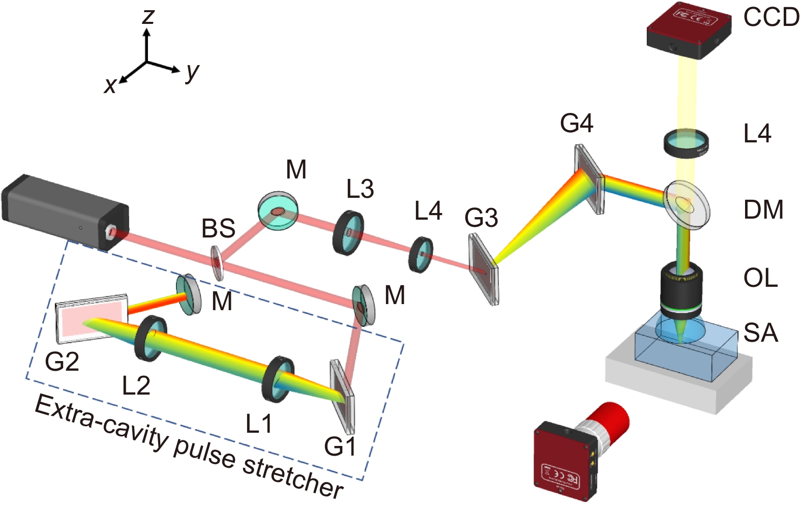
Figure 1.
Schematic of the experimental layout. BS: beam splitter; M: mirror; G1–G4: diffraction gratings; L1–L4: lenses with different focal lengths; DM: dichroic mirror; OL: objective lens; SA: sample. The dashed rectangle indicates the proposed extra-cavity pulse stretcher.
-
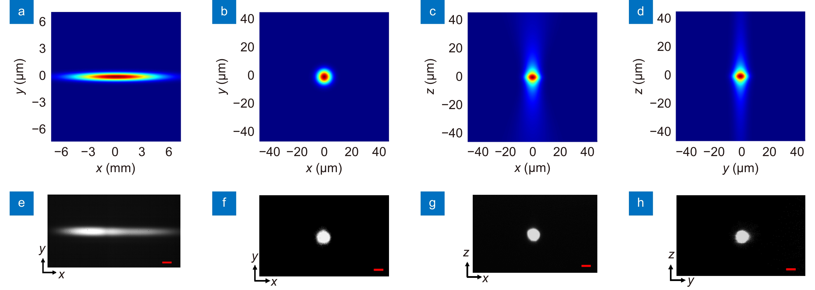
Figure 2.
(a) Numerically calculated and (e) experimentally measured laser intensity distributions at the entrance aperture of the objective lens. (b–d) Numerically calculated and (f–h) experimentally measured intensity distributions near the focus of the objective lens in XY, XZ-and YZ planes, respectively. Scale bars in (e) and (f–h) are 1 mm and 10 µm, respectively.
-
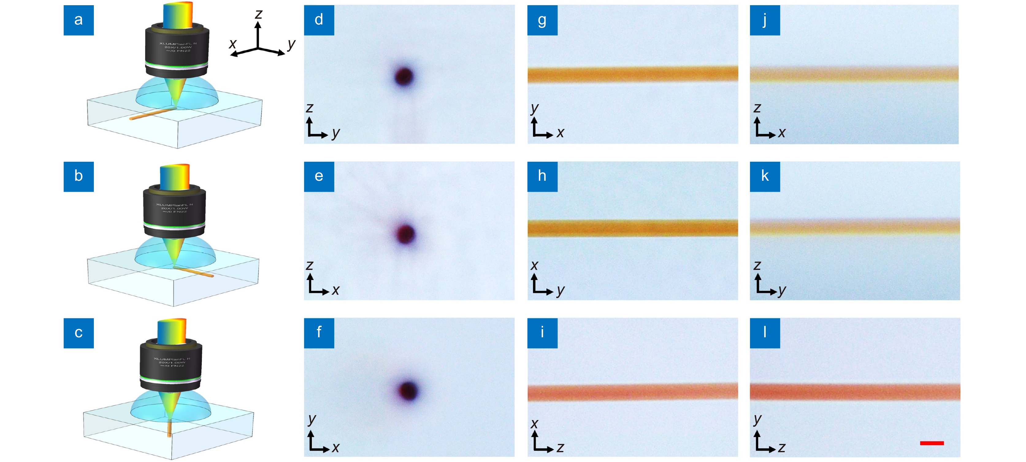
Figure 3.
Schematics of the fabrication procedure with the SSTF scheme along (a) x, (b) y, and (c) z directions, respectively. (d–f) Cross-sectional, (g–i) top-view, and (j–l) side-view optical micrographs of lines along different directions. The pulse energy and writing speed were 8 µJ and 200 µm/s, respectively. Scale bar: 20 µm.
-
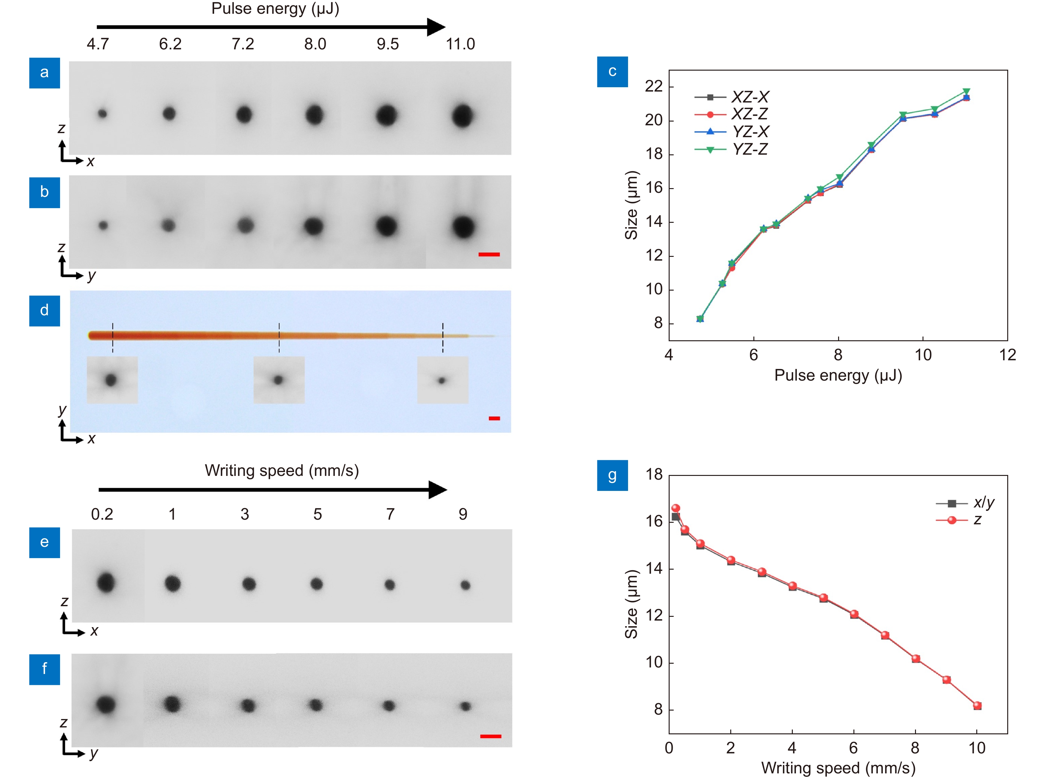
Figure 4.
The influence of pulse energy and writing speed on the fabrication resolution in the SSTF scheme. Cross-sectional optical micrographs of laser-inscribed lines in the glass along (a) y and (b) x directions with different pulse energies ranging from 4.7 µJ to 11.0 µJ. (c) Lateral and longitudinal sizes of lines in XZ and YZ planes versus pulse energies. (d) A laser-written line using segmented processing with different pulse energies ranging from 11.0 µJ to 4.7 µJ at a writing speed of 5 µm/s. The insets in (d) are the corresponding cross-sectional view optical micrographs. Cross-sectional optical micrographs of several lines inscribed along (e) y and (f) x directions at different writing speeds ranging from 0.2 mm/s to 9 mm/s, pulse energy was set at 8 µJ. (g) Lateral and longitudinal resolutions versus writing speeds. Scale bars indicate 20 µm.
-
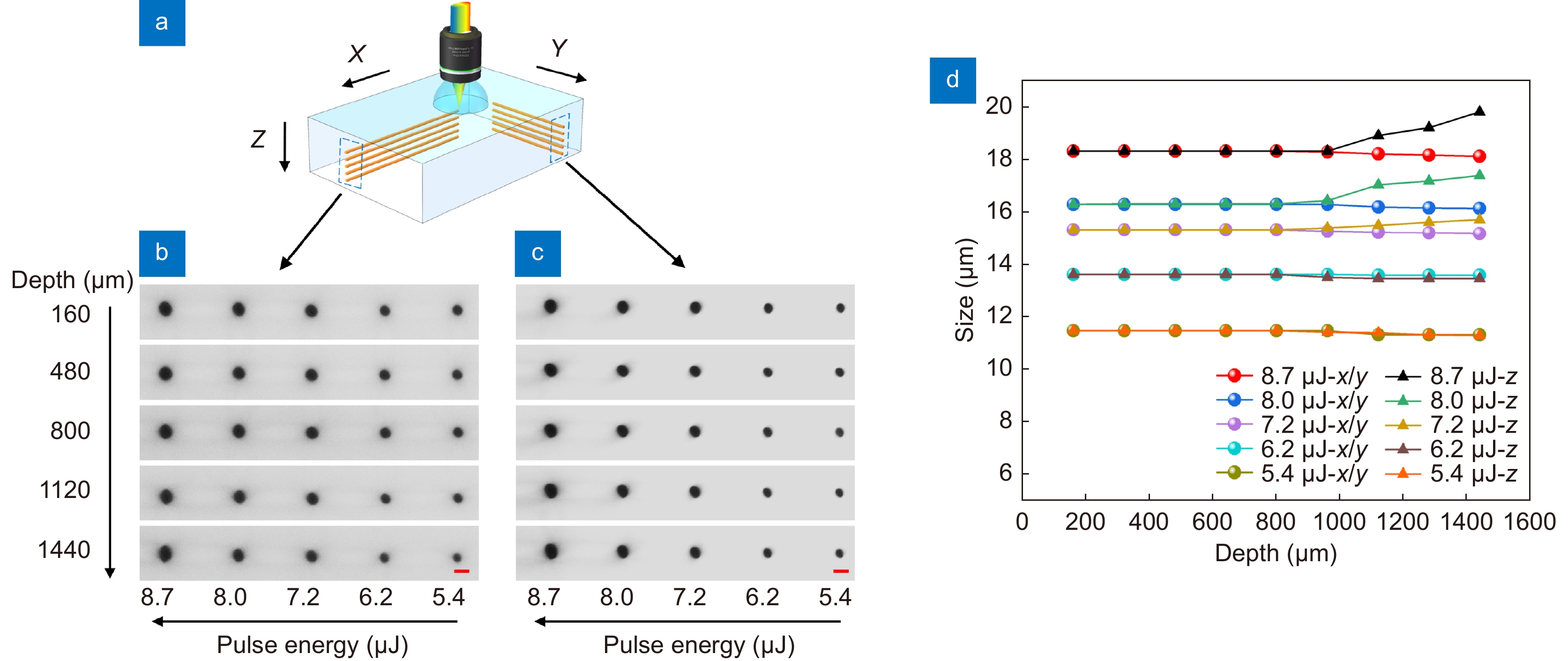
Figure 5.
The influence of processing depth on the fabrication resolution in the SSTF scheme. (a) Schematic of inscribing lines in glass at different depths along the X and Y directions. Cross-sectional optical micrographs of the lines written along the (b) X and (c) Y directions, respectively. (d) The lateral and longitudinal resolutions versus depth. Scale bar: 20 μm.
-
Figure 6.
(a) Schematic of laser-inscribed lines in the glass when the objective lens was not immersed in water. Cross-sectional optical micrographs of the lines along (b) Y and (c) X directions at different pulse energies. The pulse energies varied from 14.8 µJ to 22.8 µJ from left to right in both (b) and (c). (d) The lateral and longitudinal sizes in XZ and YZ planes versus pulse energies. Scale bar: 20 µm.
-
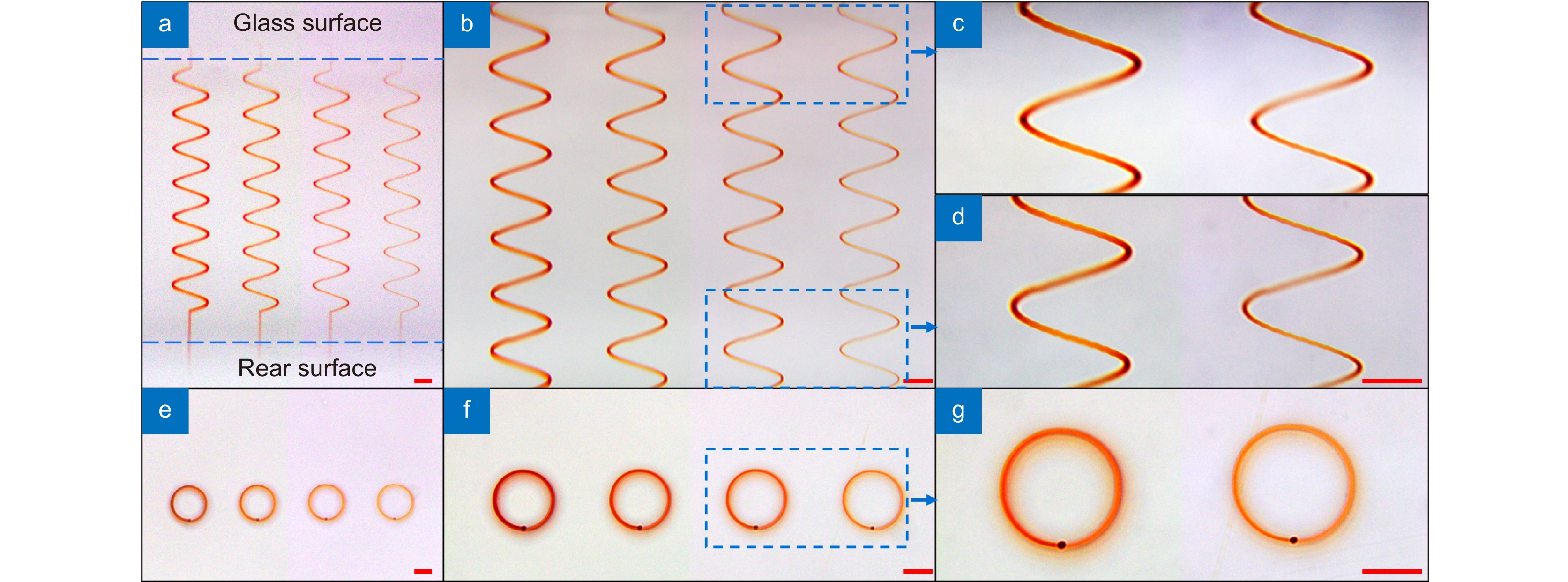
Figure 7.
(a–d) Cross-sectional view and (e–g) top-view optical micrographs of helical lines written throughout 1.6 mm thick glass at different pulse energies with the SSTF scheme. The writing speed was set at 200 μm/s, and the pulse energies from left to right were 9.5, 8.0, 7.2, and 6.2 µJ, respectively. (c) and (d) Enlarged images of (b) at different depths. (g) Enlarged image in (f). Scale bar: 100 μm.
-
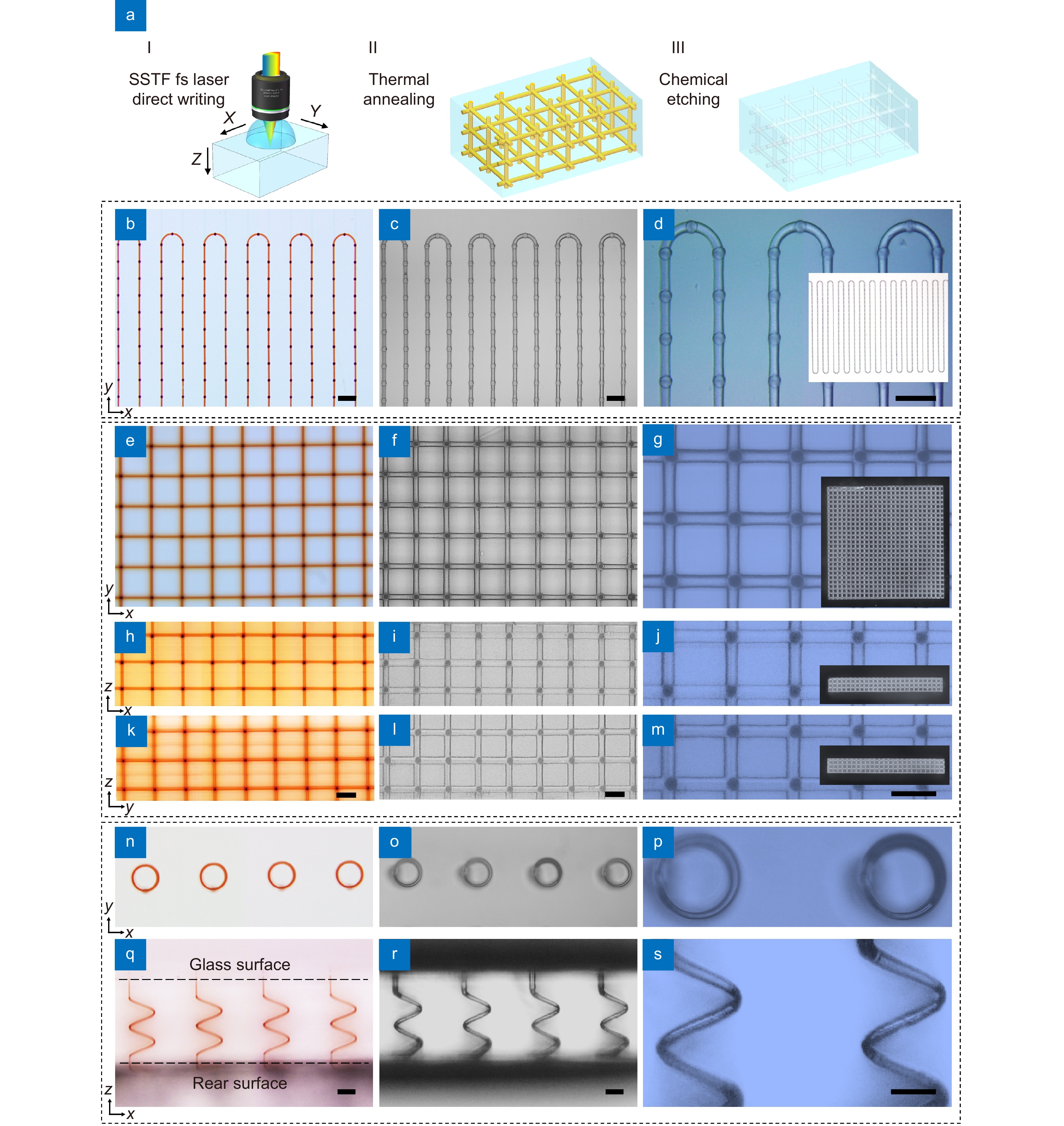
Figure 8.
(a) Schematic of the fabrication procedure for 3D microchannel structures in glass by a combination of SSTF FLDW assisted etching, which consists of three main steps: (I) SSTF fs laser direct writing; (II) thermal annealing; (III) chemical etching. (b–d) A meandering cooling structure microchannel. Optical micrographs of the channel structure (b) after FLDW followed by thermal annealing and (c) after etching. (d) An enlarged image in (c). (e–m) A 3D multilayer microchannel network structure. Optical micrographs of the 3D network structure (e, h, k) after FLDW followed by thermal annealing and after etching in XY, XZ, and YZ planes. (g, j, m) were enlarged images in (f, i, l), respectively. (n–s) 3D helical microchannel structures. The top-view (n,o) and side-view (q,r) optical micrographs of the 3D helical lines fabricated after FLDW followed by thermal annealing and after etching. (p) and (s) are enlarged images in (o) and (r), respectively. The insets in (d, g, j, m) are photographs of the microchannel structures. Scale bar: 100 μm.


