E-mail Alert
 RSS
RSS-
Abstract
Although tremendous efforts have been devoted to investigating planar single-conductor circuits, it remains challenging to provide tight confinement of electromagnetic field and compatibility with active semi-conductor components such as amplifier, harmonic generator and mixers. Single-conductor spoof surface plasmon polariton (SSPP) structure, which is one of the most promising planar single-conductor transmission media due to the outstanding field confinement, still suffers from the difficulty in integrating with the active semi-conductor components. In this paper, a new kind of odd-mode-metachannel (OMM) that can support odd-mode SSPPs is proposed to perform as the fundamental transmission channel of the single-conductor systems. By introducing zigzag decoration, the OMM can strengthen the field confinement and broaden the bandwidth of odd-mode SSPPs simultaneously. More importantly, the active semi-conductor amplifier chip integration is achieved by utilizing the intrinsic potential difference on OMM, which breaks the major obstacle in implementing the single-conductor systems. As an instance, an amplifier is successfully integrated on the single-conductor OMM, which can realize both loss compensation and signal amplification. Meanwhile, the merits of OMM including crosstalk suppression, low radar cross section (RCS), and flexibility are comprehensively demonstrated. Hence, the proposed OMM and its capability to integrate with the active semi-conductor components may provide a new avenue to future single-conductor conformal systems and smart skins.
Keywords
-
Introduction
Modern planar circuits and systems are based on the combination of multi-conductor transmission media and active semi-conductor components. However, typical multi-conductor transmission media (e.g., microstrip and coplanar waveguide) usually require large metallic ground, which leads to two limitations: 1) large metallic surfaces, especially multi-layer metallic surfaces, make the circuit too rigid to construct flexible or soft systems, and 2) large metallic surfaces increase the radar cross section (RCS) of the whole systems. To solve the problems, exploring compact single-conductor transmission media without large metallic ground is a possible path. Although single-conductor transmission media such as Goubau lines1-2 have been studied for decades, underdevelopment of single-conductor systems compared to multi-conductor ones are caused by the insufficient electromagnetic field confinement and poor compatibility with active semi-conductor technology of single-conductor media. Mature active semi-conductor components including amplifier, harmonic generator and mixers require signal input in the form of voltage. In other words, sufficient electrical potential difference in the transmission medium is necessary for active semi-conductor-component integration, which can be easily met by multi-conductor structures but is still a problem for planar single-conductor media.
Similar to traditional microwave transmission media, multi-conductor ultra-thin SSPP technology grows rapidly and displays vitality of this field. The landmark achievement of sub-diffraction-limited signal wireless communication carried by the multi-conductor SSPP system45 demonstrates the superiority of SSPPs. Nevertheless, multi-conductor ultra-thin SSPP technology provides no obvious advantages in breaking the two limitations of multi-conductor transmission media mentioned above. Meanwhile, although single-conductor SSPPs have been proved to possess the ability of field confinement and conformal propagation, they are still far away from systematic applications because there is no good method to integrate key active semi-conductor components such as amplifier46 into single-conductor SSPP circuits. Thus, seeking a feasible method to solve the problems of multi-conductor transmission media and break the bottleneck of single-conductor transmission media simultaneously is still urgent.
In this paper, we propose a new kind of odd-mode-metachannel (OMM) for single-conductor systems. Firstly, potential of active semi-conductor-component integration is theoretically analyzed. Then, basic design principle of the OMM to strengthen field confinement and broaden bandwidth simultaneously is presented. Further, a single-conductor amplifier integrated in OMM is achieved by utilizing odd-mode field potential difference of the OMM. It should be noted that the proposed amplifier integration method can be extended into almost all active semi-conductor components in microwave and terahertz systems. Meanwhile, three merits of crosstalk suppression based on odd-even-mode orthogonality, low RCS and flexibility of the OMM are demonstrated as well. Hence, the proposed OMM may overcome the obstacles of realizing single-conductor systems and provide one more avenue to future smart skins.
Spoof surface plasmon polaritons (SSPPs)3-11 are special type of surface waves which can mimic the optical natural surface plasmon polaritons (SPPs)12-16, and can be supported by both single-conductor and multi-conductor plasmonic metamaterials in microwave and terahertz bands through specially decorated metallic surfaces or strips17-23. Due to the properties of field confinement, controllable dispersion and great compatibility with planar circuit technology, ultra-thin SSPP structures have been proved to possess many merits in microwave and terahertz engineering such as low crosstalk24-29, minimized packaging30, 31, low RCS32 and low-cost electromagnetic protection33. Based on these merits, SSPPs are utilized to realize a series of novel devices including filters34-36, modulators37, 38, antennas39-43, and even landmark systems such as wireless body sensor networks44 and wireless communication system45.
Results and discussions
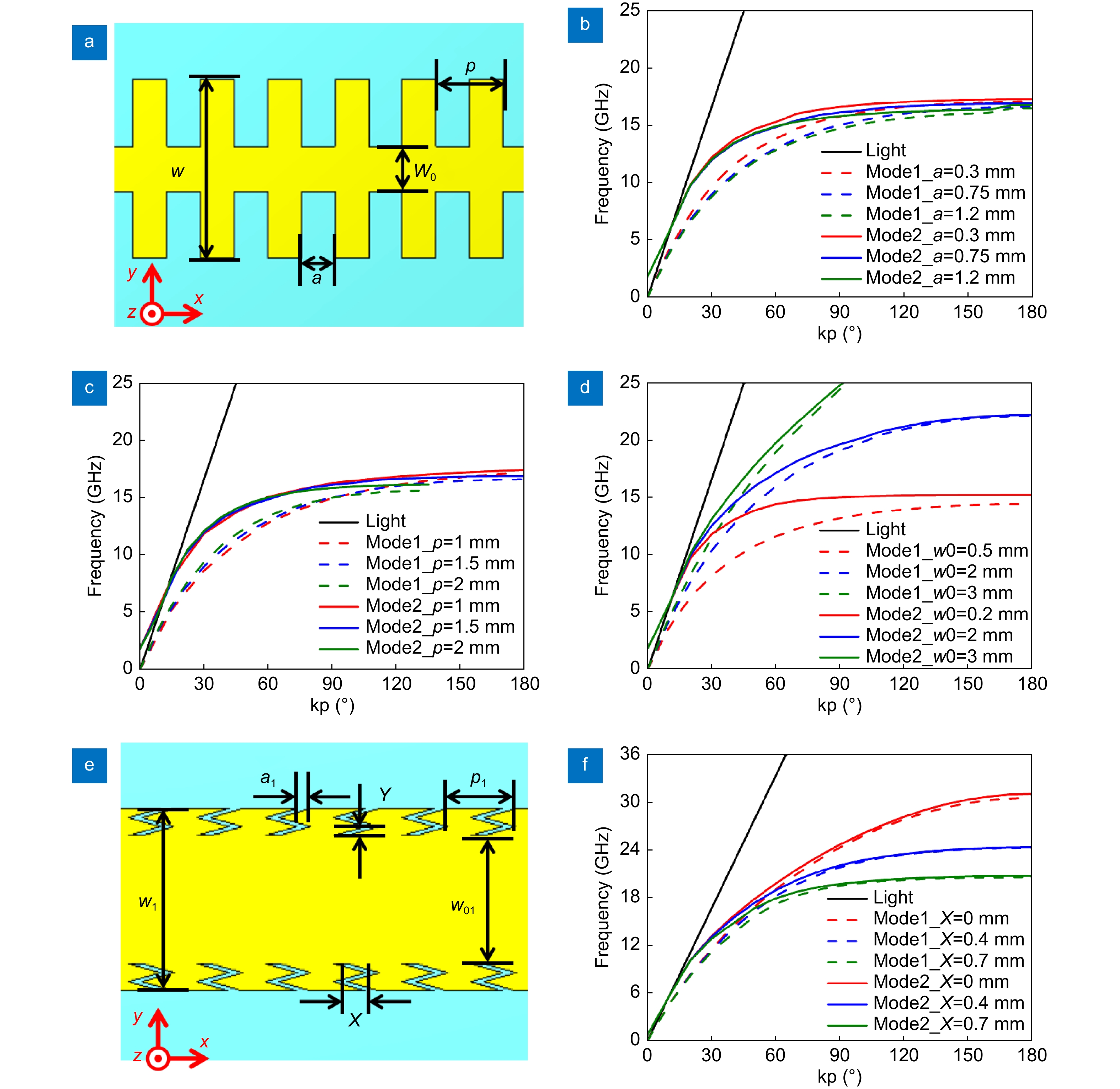
![Figure 3. Geometrical parameters and dispersion curves of the typical SSPP waveguide and the OMM. (a) Geometrical parameters of the typical SSPP structure, where the width of the center strip is w fixed as 4 mm, the period of the unit is p, the width of the grooves is a and the width of the narrow strip is w0. (b) Dispersion curves of the typical SSPP structure with varying a, where p = 1.5 mm, w0 = 1 mm. (c) Dispersion curves of the typical SSPP structure with varying p, where a = 0.75 mm and w0 = 1 mm. (d) Dispersion curves of the typical SSPP structure with varying w0, where p = 1.5 mm, a = 0.75 mm. (e) Geometrical parameters of the OMM, where the width of the center strip is w1 fixed as 4 mm, the period of the unit is p1, the width of the narrow strip is w01, the folding extent of the zigzag grooves is described by X and Y. (f) Dispersion curves of the typical SSPP structure with varying X, where w1 = 4 mm, w01 = 2.8 mm, a1 = 0.3 mm, p1 = 1.5 mm, Y=0.2 mm.]()
Geometrical parameters and dispersion curves of the typical SSPP waveguide and the OMM. (a) Geometrical parameters of the typical SSPP structure, where the width of the center strip is w fixed as 4 mm, the period of the unit is p, the width of the grooves is a and the width of the narrow strip is w0. (b) Dispersion curves of the typical SSPP structure with varying a, where p = 1.5 mm, w0 = 1 mm. (c) Dispersion curves of the typical SSPP structure with varying p, where a = 0.75 mm and w0 = 1 mm. (d) Dispersion curves of the typical SSPP structure with varying w0, where p = 1.5 mm, a = 0.75 mm. (e) Geometrical parameters of the OMM, where the width of the center strip is w1 fixed as 4 mm, the period of the unit is p1, the width of the narrow strip is w01, the folding extent of the zigzag grooves is described by X and Y. (f) Dispersion curves of the typical SSPP structure with varying X, where w1 = 4 mm, w01 = 2.8 mm, a1 = 0.3 mm, p1 = 1.5 mm, Y=0.2 mm.
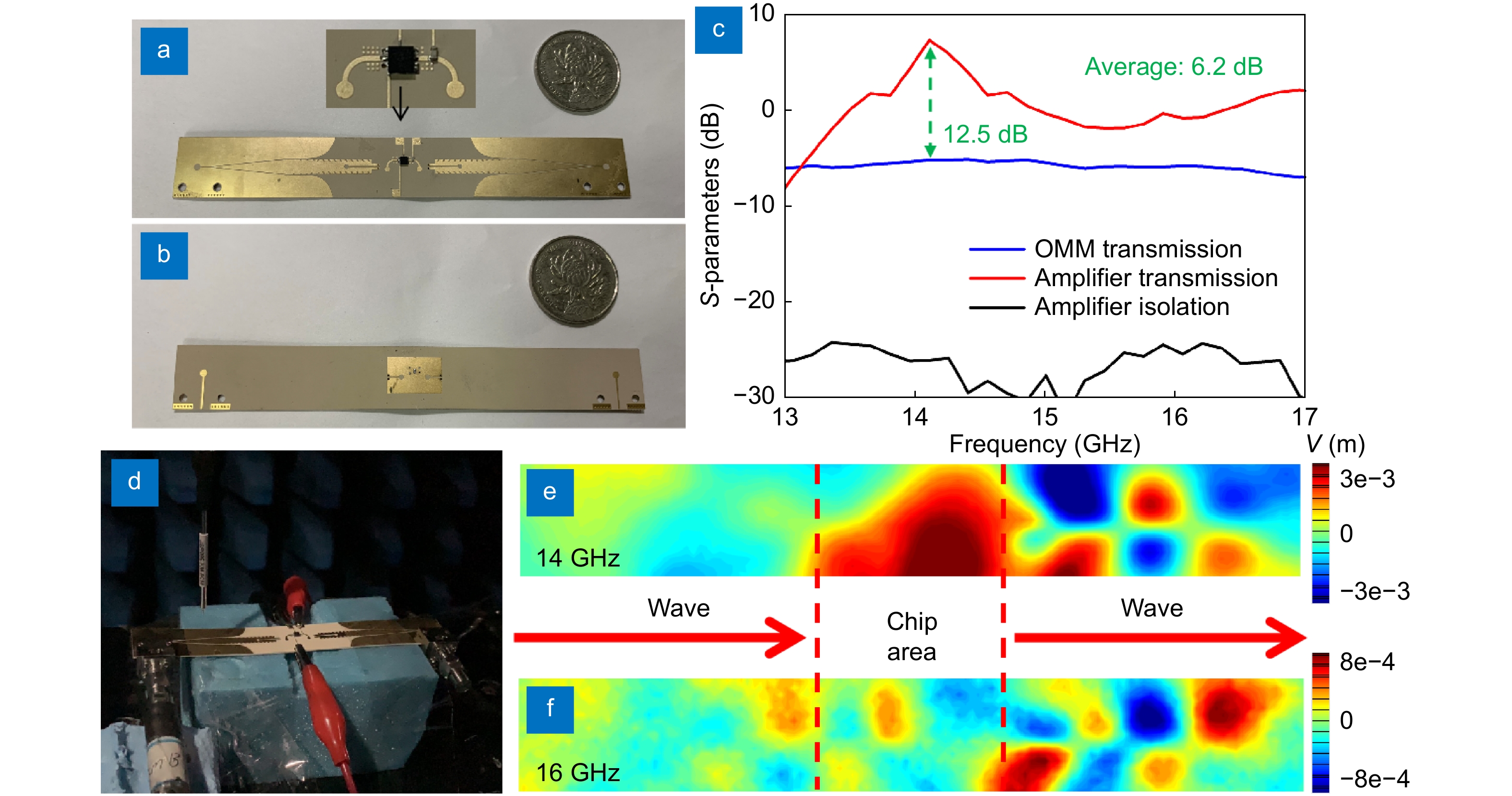
![Figure 7. Experiments of the amplifier-integrated OMM. (a) Top view of the sample. (b) Bottom view of the sample. (c) Measured S-parameters of the sample. (d) The photograph of the EM scanning system composed of a VNA and a monopole probe installed in a mechanical platform in an EM shielding chamber. (e, f) The measured near-electric-field distributions of the amplifier-integrated OMM sample at (e) 14 and (f) 16 GHz.]()
Experiments of the amplifier-integrated OMM. (a) Top view of the sample. (b) Bottom view of the sample. (c) Measured S-parameters of the sample. (d) The photograph of the EM scanning system composed of a VNA and a monopole probe installed in a mechanical platform in an EM shielding chamber. (e, f) The measured near-electric-field distributions of the amplifier-integrated OMM sample at (e) 14 and (f) 16 GHz.
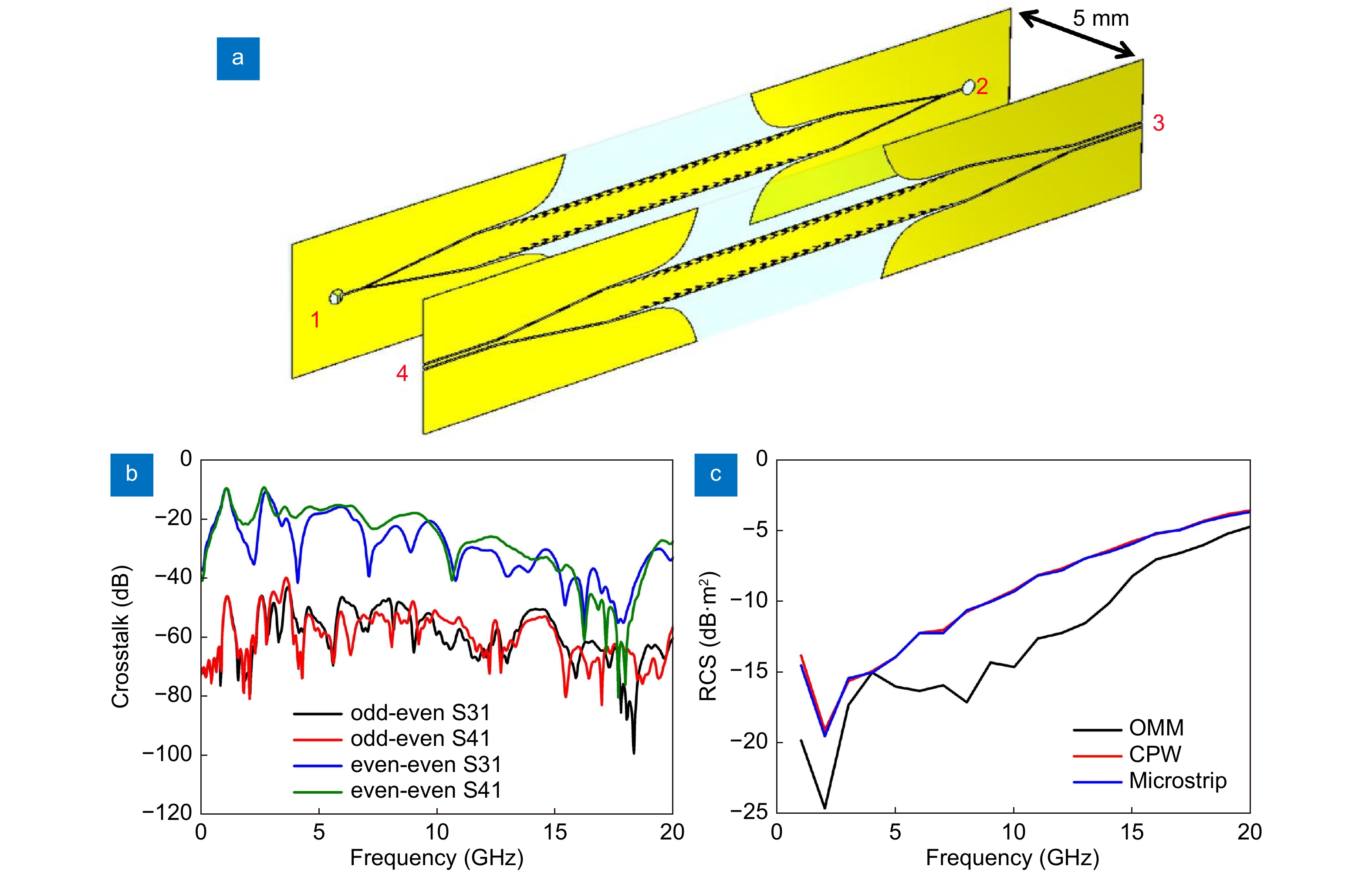
In addition to the strengthened field confinement and active semi-conductor-component integration, we discuss three more advantages of the OMM for single-conductor systems as well. First, we investigate crosstalk suppression of the OMM based on odd-even-mode orthogonality. As shown in Fig. 3, the proposed OMM can support not only odd-mode but also even-mode SSPPs. Considering the case of plane antenna array, feeding waveguides may be arranged parallel as shown in Fig. 8(a). A typical 50 Ω CPW excitation of the even-mode SSPP channel is selected. By arranging the two channels in a distance of 5 mm, the crosstalk of typical even-even and odd-even coupling pairs are compared, as shown in Fig. 8(b) to 8(e). It is observed that average crosstalk suppression of about 30 dB can be realized utilizing the odd-even-mode orthogonality of the proposed OMM.
where C1 and C2 are two constants, ω is the frequency, ε0 is the permittivity of vacuum, km is the wave number of the metal and β is the propagation coefficient of the SPP mode. The electrical potential difference between the two surfaces of metal can be calculated by
![Figure 9. Flexibility test of the amplifier-integrated OMM.]()
Flexibility test of the amplifier-integrated OMM.
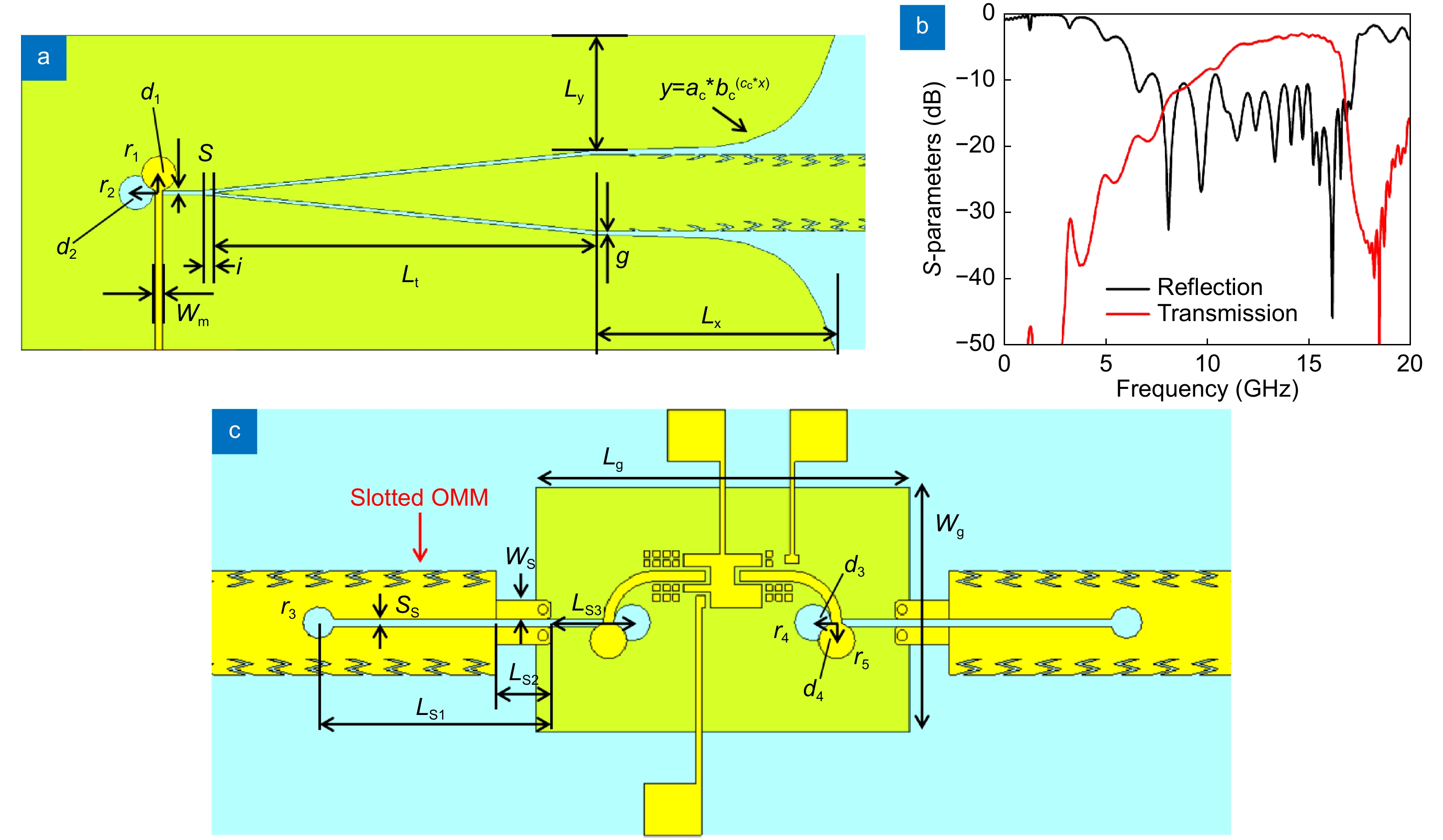
For experimental demonstrating the active semi-conductor-component integration of the proposed OMM, a sample of amplifier-integrated OMM with total length of 122.3 mm is fabricated, as shown in Fig. 7(a) and 7(b). Here, a broadband low noise amplifier chip MAAL-011130 is used as the instance of active semi-conductor component due to its compact package size and appropriate working band. In the experiment, standard 2.40 mm JACK (FEMALE) end launch connector is used to connect two ports of the sample and coaxial cables of the vector network analyzer (VNA) AV3672B. Measured S-parameters of the sample are shown in Fig. 7(c). Compared to a pure OMM with nearly the same length of 123 mm, average gain of about 6.2 dB in the main band (13 to 17 GHz) of the OMM and peak gain of 12.5 dB at 14.1 GHz can be obtained, which demonstrates successful integration of the OMM and amplifier chip. To visualize the amplification of odd-mode SSPPs, near-electric-field distributions of the sample are measured using an EM scanning system composed of a VNA and a monopole probe installed in a mechanical platform in an EM chamber, as shown in Fig. 7(d). In Fig. 7(e) to 7(g), measure near-electric-field distribution of the sample at 14 and 16 GHz are exhibited, where the odd-mode field and transmission gain can be observed visually. In fact, this integration method based on the novel field nature of OMMs can be extended to almost all active semi-conductor components required in wireless communication or radar systems, such as power amplifiers and harmonic generators.
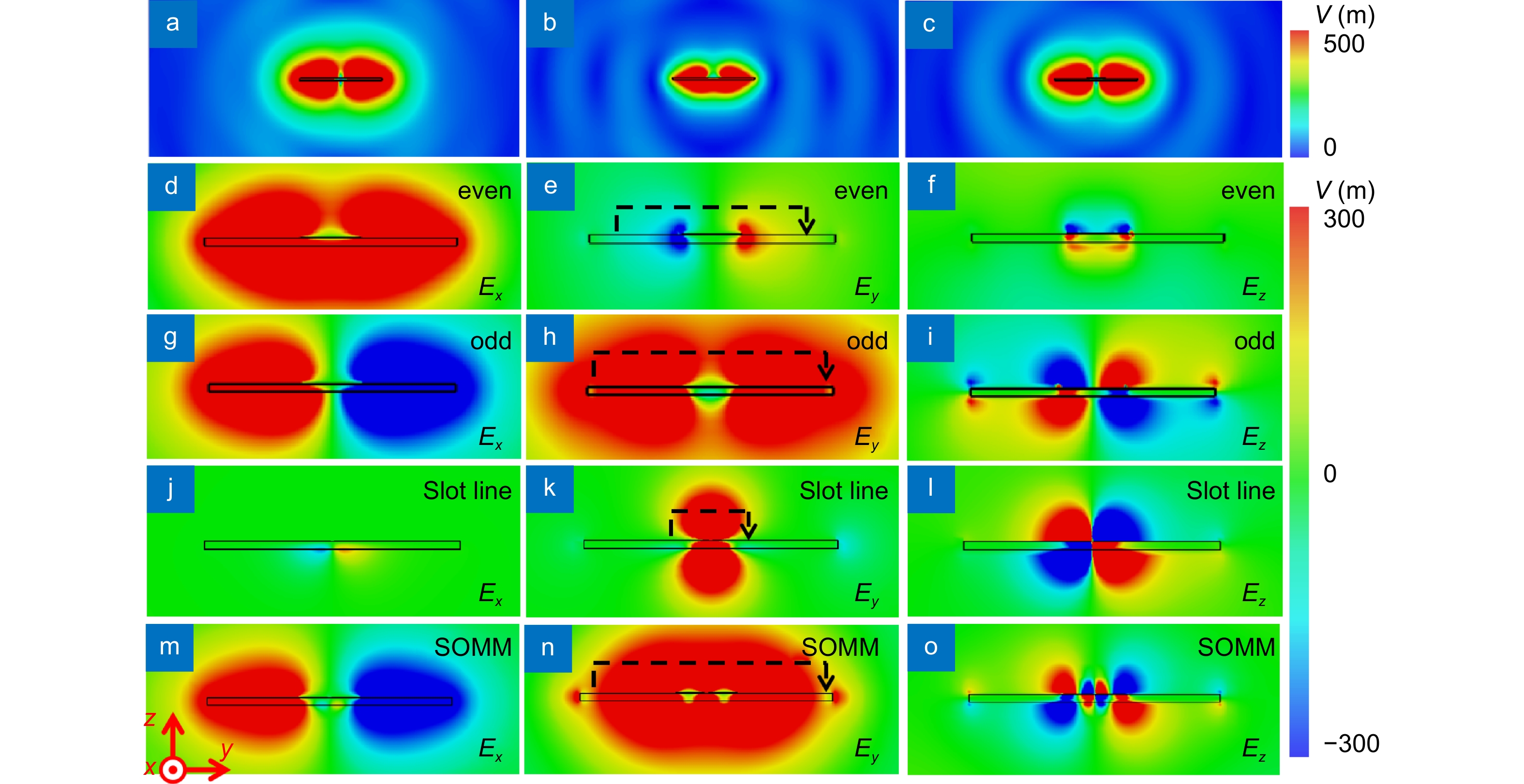
where k and k0 are the wavenumber of the SSPP mode and free space mode, respectively. Absolute-value electric-field distributions on the cross section of the typical SSPP (X = 0 mm) waveguide and the OMM (X = 0.7 mm) are shown in Fig. 5(a) to 5(c), which visually demonstrate the strengthened field confinement for both even- and odd-mode SSPPs led by introducing zigzag grooves.
{E_z} = {C_1}\frac{\beta }{{\omega {ε _0}{ε _{\rm{m}}}}}{{\rm{e}}^{{\rm{j}}\beta x}}{{\rm{e}}^{{k_{\rm{m}}}z}} + {C_2}\frac{\beta }{{\omega {ε _0}{ε _{\rm{m}}}}}{{\rm{e}}^{{\rm{j}}\beta x}}{{\rm{e}}^{ - {k_{\rm{m}}}z}} \;, ![Figure 8. Crosstalk suppression and low RCS properties of the OMM. (a) Coupling pair of SSPP channel. (b) Crosstalk of typical even-even coupling pair and odd-even coupling pair. (c) RCS of the OMM compared to that of a CPW with the same total size.]()
Crosstalk suppression and low RCS properties of the OMM. (a) Coupling pair of SSPP channel. (b) Crosstalk of typical even-even coupling pair and odd-even coupling pair. (c) RCS of the OMM compared to that of a CPW with the same total size.
Normalized field integral of different modes.
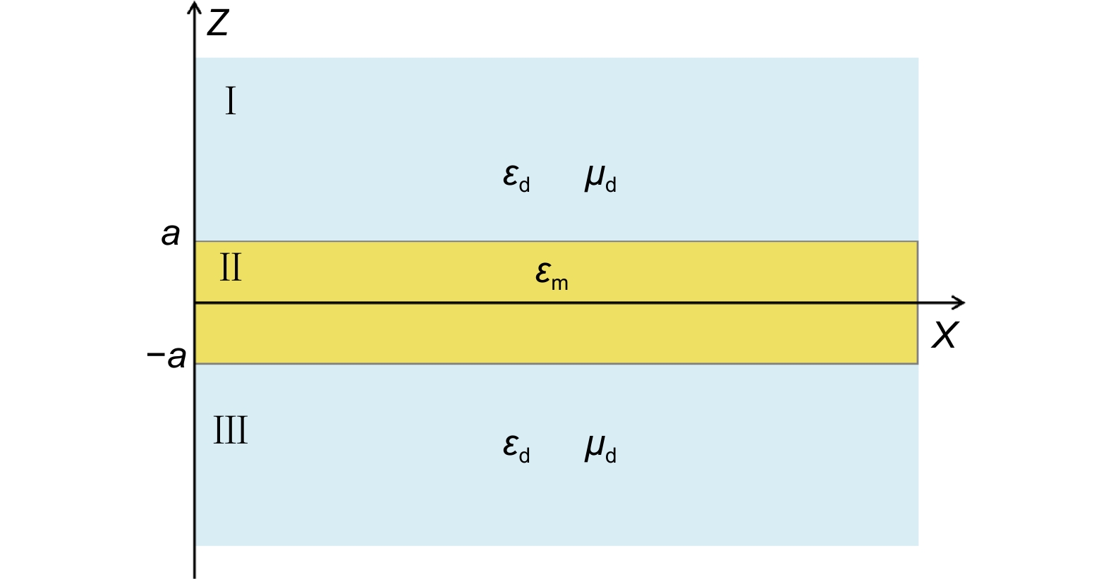
Parameters Ex Ey Ez Even mode of the OMM 18.5073 0.0012 1 Odd mode of the OMM 0.5273 25.8723 1 Odd mode of the SOMM 2.995 93.139 1 Mode of the slot line 0.16 11.6556 1 ![Figure 1. The insulator-metal-insulator model.]()
The insulator-metal-insulator model.
v = \sqrt {{k^2} + k_0^2} \;, For exciting the OMM efficiently, a conversion structure to convert traditional quasi-transverse electromagnetic (quasi-TEM) mode and odd-mode SSPPs, as shown in Fig. 6(a). Using a microstrip-slot transition, the even quasi-TEM mode is transferred into odd slot mode. Then the odd-mode signal on the slot is coupled onto a tapered coplanar waveguide and transferred into the odd-mode SSPPs through gradient grooves and flaring grounds. The geometrical details are listed in Table 1. Through mirror replication of the conversion structure in Fig. 6(a), both ends of the OMM are transferred to microstrip ports, which is convenient for coaxial cable feeding. Transmission and reflection performances of the conversion structure is shown in Fig. 6(b), where the length of the OMM is 30 mm (20 units). A broad reflection band from 9.4 to 17.7 GHz and desired transmission efficiency in the main field-confinement band from 13 to 17 GHz are observed. The odd-mode SSPPs at low frequencies possess too weak field confinement ability to keep energy propagating, and those near the higher cutoff frequency suffer from the dielectric and metallic loss. Thus, the band from 13 to 17 GHz is the main band of the OMM.
{h_{\rm{e}}} = \left( {{w_1} - {w_{01}}} \right) \cdot {{\sqrt {{X^2} + {Y^2}} } / {2Y}}\;. The analysis of insulator-metal-insulator model is different from the SSPP cases but can qualitatively inspire the idea of using odd-mode SSPPs to provide internal electrical potential difference. Hence, we propose the idea of utilizing odd-mode SSPPs to achieve active semi-conductor-component integration, as indicated in Fig. 2.
The Ez field in region II (–a ≤
z ≤ a) can be expressed as V = \int_{ - a}^a {{E_z}} {\rm{d}}z \;. Integration of active semi-conductor components is the key step to implement system construction. Utilizing odd-mode property of the OMM, a compact conversion structure is designed to convert odd-mode SSPP waves into voltage input of chips, as shown in Fig. 6(c). The OMM is converted into a slot line through a slotted OMM (SOMM) whose electric-field distributions are shown in Fig. 5(m–o). Then a typical slot-microstrip transition can be used to realize standard input/output port for packaged chips. Detailed geometrical parameters of the conversion structure are listed in Table 1 as well. Quantitatively, cross-section field integral of different modes in Fig. 5 and odd mode of the SOMM are listed in Table 2 to demonstrate the similarity of odd-mode OMM and slot line. Integral of all field components are normalized to that of Ez. Slot line supports a nearly transverse electrical (TE) mode which possesses small integral value of Ex and great integral value of Ey. It can be observed from Table 2 that even mode of the OMM is greatly different from mode of the slot line, while odd mode of the OMM and odd mode of the SOMM possess similar property with that of the slot line.
According to the continuity of Ex and Hy at the boundary of the upper surface (z =
a) and the lower surface (z = –a), an even mode requires that C1 = –C2. Then, it is easy to know that the electrical potential difference V for the even mode is 0, which indicates that the even-mode SPPs in the model cannot support internal electrical potential difference. However, for an odd mode where C1 = C2, the non-zero electrical potential difference V can be calculated by ![Figure 6. The conversion structures. (a) Conversion structure between the quasi-TEM mode and odd-mode SSPPs, where 5 linearly gradient SSPP units are employed. (b) Simulated S-parameters of the conversion structure, where the OMM is composed of 46 units. (c) The compact conversion structure to convert odd-mode SSPP waves into voltage input of chips.]()
The conversion structures. (a) Conversion structure between the quasi-TEM mode and odd-mode SSPPs, where 5 linearly gradient SSPP units are employed. (b) Simulated S-parameters of the conversion structure, where the OMM is composed of 46 units. (c) The compact conversion structure to convert odd-mode SSPP waves into voltage input of chips.
Geometrical parameters of the conversion structures.
Parameters Values (mm) Parameters Values Parameters Values(mm) Parameters Values (mm) r1 0.9 Lt 20 mm r3 0.6 r4 0.7 r2 0.9 Lx 12.5 mm Ss 0.3 r5 0.7 d1 1 Ly 6 mm Ls1 8.85 d3 0.9 d2 1.2 ac 0.00587 Ls2 2.1 d4 0.7 S 0.2 bc 2 Ls3 3.1 Wg 9.4 Wm 0.4 cc 0.8 Ws 0.7 i 0.6 g 0.2 mm Lg 14.3 Then, we reveal the tradeoff between broadening bandwidth and strengthening field confinement of single-conductor odd-mode SSPPs. Typical single-conductor ultra-thin SSPP structure is constructed by a metallic strip with periodic comb grooves, as shown in Fig. 3(a). The substrate is a Rogers RO3010 board with relative permittivity εr = 11.2, loss tangent tanδ = 0.0022 and thickness of 0.508 mm. This structure can support the even mode (mode 1) and the odd mode (mode 2) of SSPPs, which can be visually observed in Fig. 4. Different from the even-mode SSPPs that works in the band from 0 GHz to the cutoff frequency, the odd-mode SSPPs possess narrow-band-pass nature because the single-conductor strip could shorten the odd-mode waves at low frequencies. The stop band of odd-mode SSPPs can be estimated by the split of the even- and odd-mode as well since the odd mode far away from the even mode will approach a radiating mode. Figure 3(b) to 3(d) exhibit the dispersion curves of SSPPs under varying geometrical parameters, where the total width w is fixed as 4 mm. Here, all the dispersion curves are normalized to p = 1.5 mm because the change of p in Fig. 3(c) will affect the dispersion curves observation. It can be easily observed in Fig. 3(d) that split of the even- and odd-mode SSPPs is dominated by the width of the narrow strip w0. Increasing w0 can decrease the lower cutoff frequency but simultaneously weaken the field confinement of the odd-mode SSPPs since the depth of the grooves is decreased as well. Thus, there is a tradeoff between broadening bandwidth and strengthening field confinement of odd-mode SSPPs with the fixed transverse width w.
Since it is hard to analyze ultra-thin SSPP structures with complex geometrical using analytical expressions, a brief discussion of odd-mode SPPs in the insulator-metal-insulator model47 is carried out to provide a qualitative reference of odd-mode SSPPs, as shown in Fig. 1. In this model, insulator in region I (z > a) and region III(z < –a) are identical and with the relative permittivity of εd, and metal in region II (–a ≤ z ≤ a) are with the permittivity of εm. SPP waves propagate along the x direction.
Second, for revealing the low RCS merits of the single-conductor OMM, simulated RCS results of the OMM, a CPW and a microstrip board with the same total size are shown in Fig. 8(c). It is observed that the CPW and microstrip board possess nearly the same RCS because their metallic areas are almost identical. Since the ratio of the metallic surface area of the OMM to that of the CPW is near 1:2, the RCS of the OMM is lower than the CPW board by about 3 dB on average.
Here, we propose a new OMM with zigzag grooves, as shown in Fig. 3(e). Zigzag grooves are introduced into the OMM to strengthen the field confinement. Unit structure in Fig. 3(e) is with width w1 = 4 mm, period p1 = 1.5 mm and width of the narrow strip w01 =2.8 mm. Folding extent of the zigzag grooves is described by X and Y. The geometrical equivalent depth of zigzag grooves he, can be expressed as
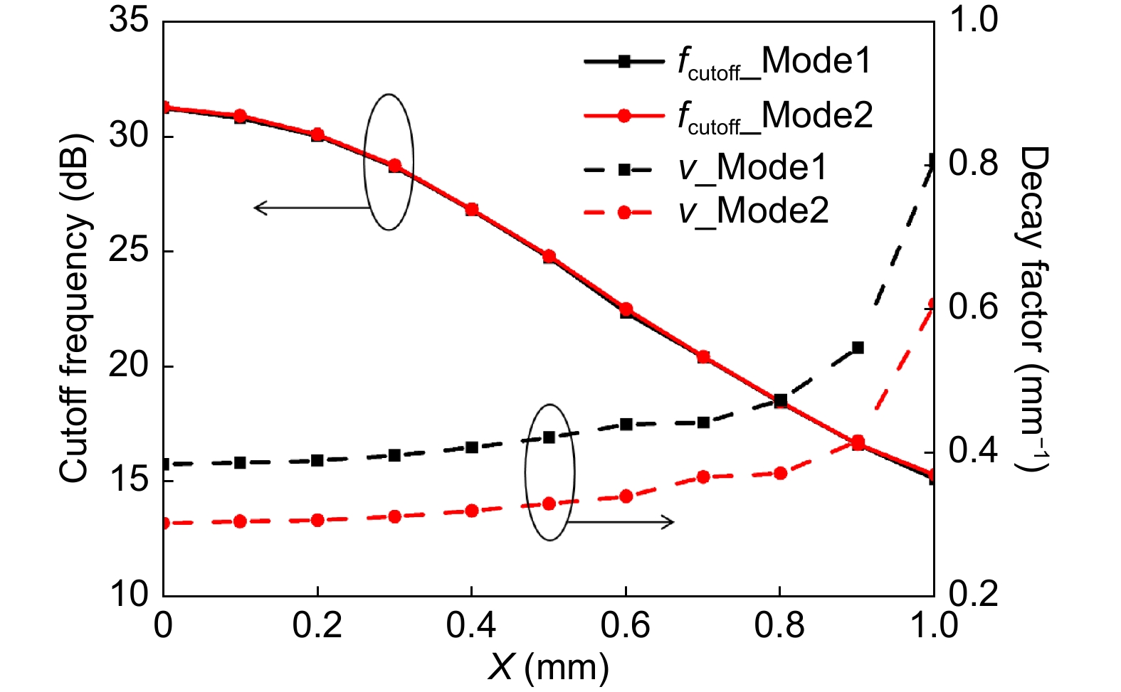
V = {C_1}\frac{{2\beta }}{{\omega {ε _0}{ε _{\rm{m}}}{k_{\rm{m}}}}}{{\rm{e}}^{{\rm{j}}\beta x}}\left( {{{\rm{e}}^{{k_{\rm{m}}}a}} - {{\rm{e}}^{ - {k_{\rm{m}}}a}}} \right) \;. ![Figure 4. Cutoff frequency and decay factor curves with varying X, where the other parameters are the same with those in Fig. 3(f).]()
Cutoff frequency and decay factor curves with varying X, where the other parameters are the same with those in Fig. 3(f).
![Figure 5. Electric-field distributions of the cross sections of the SSPP structures at 15 GHz. (a–c) Absolute value of electric-field distributions on the cross-section of (a) even-mode of the typical SSPP (X = 0 mm) waveguide, (b) even mode and (c) odd mode of the OMM (X = 0.7 mm). (d) X-component, (e) Y-component and (f) Z-component of electric field of even mode of the OMM. (g) X-component, (h) Y-component and (i) Z-component of electric field of odd mode of the OMM. (j) X-component, (k) Y-component and (l) Z-component of electric field of slot line. (m) X-component, (n) Y-component and (o) Z-component of electric field of SOMM.]()
Electric-field distributions of the cross sections of the SSPP structures at 15 GHz. (a–c) Absolute value of electric-field distributions on the cross-section of (a) even-mode of the typical SSPP (X = 0 mm) waveguide, (b) even mode and (c) odd mode of the OMM (X = 0.7 mm). (d) X-component, (e) Y-component and (f) Z-component of electric field of even mode of the OMM. (g) X-component, (h) Y-component and (i) Z-component of electric field of odd mode of the OMM. (j) X-component, (k) Y-component and (l) Z-component of electric field of slot line. (m) X-component, (n) Y-component and (o) Z-component of electric field of SOMM.
Flexibility test of gain (dB) of the amplifier-integrated OMM.
Radius 13 GHz 14 GHz 15 GHz 16 GHz 17 GHz 11 cm 3.5 16.2 13.1 6.3 16.8 14 cm 3.4 15.8 13.7 7.3 16.7 22 cm 6.0 22.3 17.5 14.9 18.9 It is worth noting that although even-mode SSPPs can be converted into CPW or microstrip ports to connect packaged chips, cumbersome conversion structures occupying large spaces are required because the potential difference exists between the even-mode SSPP waveguide and infinity, which is vastly different from that of typical chip input port. Combining all the designed sections, the whole amplifier-integrated OMM is shown in Fig. 2.
It can be observed from Eq. (4) that even though large w01 limits the space of grooves, the equivalent depth of zigzag grooves can still be enlarged by increasing the folding extent. Figure 3(f) shows the dispersion curves of the OMM with varying X and fixed w1, w01, a1, p1 and Y. The field confinement is obviously improved by enlarging X while the lower cutoff frequency of the odd mode will not increase, which indicates that broadening bandwidth and strengthening field confinement of single-conductor odd-mode SSPPs can be realized simultaneously. Quantitatively, cutoff frequency and decay factor with varying X are shown in Fig. 4, where the decay factor v is calculated by
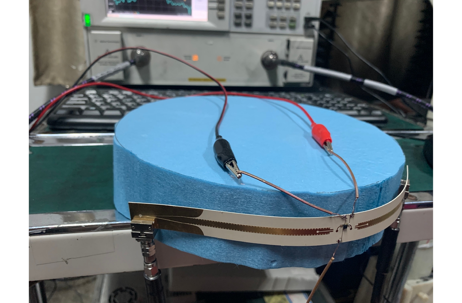
At last, the flexibility of the amplifier-integrated OMM is tested as well. A lengthened sample with the length of 236.3 mm is bent on a foam cylinder with near-air electric properties and different radius r, as shown in Fig. 9. Measured gains of the amplifier-integrated OMM with different bending radius compared to a pure OMM with nearly the same length of 237 mm are listed in Table 3. It can be observed that the OMM can be easily bent to a dramatic angle, which is difficult for traditional microstrips or CPWs with large and rigid metallic surfaces in the view of mechanics. Meanwhile, efficient gain performance of the amplifier-integrated OMM can be maintained under large-angle bending. Hence, the OMM is verified to be adequate for conformal applications as well.
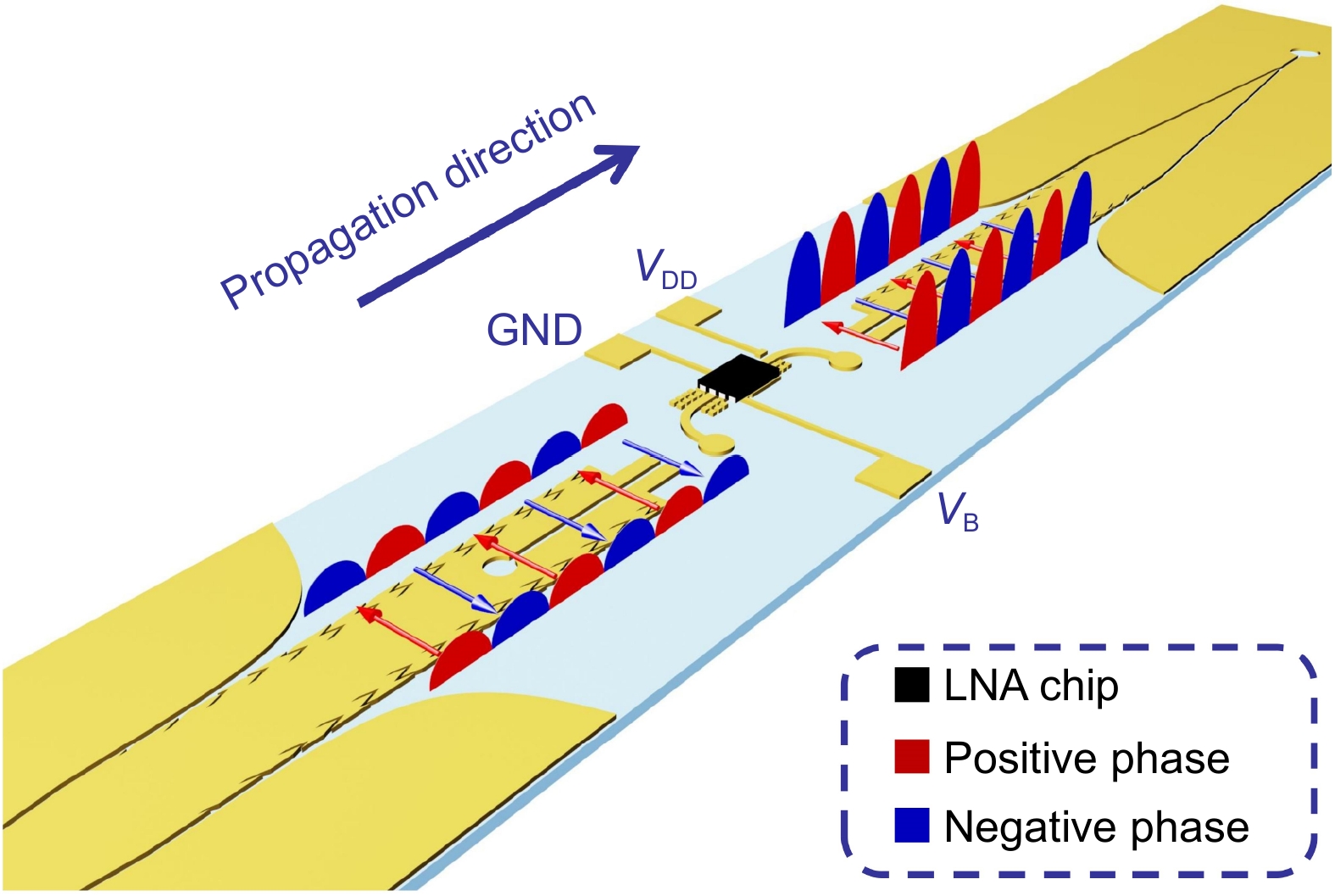
![Figure 2. Schematic diagram of the whole amplifier-integrated OMM.]()
Schematic diagram of the whole amplifier-integrated OMM.
To investigate the mode similarity of the OMM and traditional multi-conductor transmission medium (e. g. slot line) that can provide voltage input for active semi-conductor components, detailed electric-field component distributions of the OMM and the slot line are exhibited in Fig. 5(d–l). It can be observed that even-mode SSPP possesses zero potential difference between the two sides of the metachannel, because the integral of Y-component along the dash line in Fig. 5(e) is 0. In contrast, the integral of Y-component along the imaginary line of odd-mode SSPP in Fig. 5(h) has non-zero value, which is similar to the slot line. Hence, the similarity of single-conductor OMM and slot line indicates that the OMM can be easily converted into an active semi-conductor-component port with voltage input or output.
Conclusions
This paper proposes a new kind of odd-mode-metachannel to perform as the fundamental transmission medium for single-conductor system. Basic designing tradeoff of bandwidth and field confinement of odd-mode SSPPs is resolved by introducing zigzag decorations onto the SSPP structure. Merits including low RCS, crosstalk suppression and flexibility of the OMM are verified. Utilizing the intrinsic potential difference on the OMM, novel integration between planar single-conductor medium and active semi-conductor component is achieved, which is difficult in traditional view. Beyond the single-conductor area, it is also possible to extend the idea of utilizing odd-mode field to excite active semi-conductor components into multi-conductor areas such as integrated circuit design. In conclusion, the proposed OMM and the method of active semi-conductor-component integration remove the major obstacles of realizing conformal single-conductor systems and provide an avenue to future smart skins.
Acknowledgements
We are grateful for financial supports from the National Natural Science Foundation of China under Grant Nos. 62101122, 61871127, 61701108 and 61631007, Natural Science Foundation of Jiangsu Province under Grant BK20210212, and the 111 Project under Grant No. 111-2-05.
Competing interests
The authors declare no competing financial interests.
-
References
[1] Goubau G. Open wire lines. IRE Trans Microw Theory Tech 4, 197–200 (1956).
DOI: 10.1109/TMTT.1956.1125062[2] Akalin T, Treizebré A, Bocquet B. Single-wire transmission lines at terahertz frequencies. IEEE Trans Microw Theory Tech 54, 2762–2767 (2006).
DOI: 10.1109/TMTT.2006.874890[3] Pendry JB, Martín-Moreno L, Garcia-Vidal FJ. Mimicking surface plasmons with structured surfaces. Science 305, 847–848 (2004).
DOI: 10.1126/science.1098999[4] Hibbins AP, Evans BR, Sambles JR. Experimental verification of designer surface plasmons. Science 308, 670–672 (2005).
DOI: 10.1126/science.1109043[5] Yu NF, Wang QJ, Kats MA, Fan JA, Khanna SP et al. Designer spoof surface Plasmon structures collimate terahertz laser beams. Nat Mater 9, 730–735 (2010).
DOI: 10.1038/nmat2822[6] Kats MA, Woolf D, Blanchard R, Yu NF, Capasso F. Spoof Plasmon analogue of metal-insulator-metal waveguides. Opt Express 19, 14860–14870 (2011).
DOI: 10.1364/OE.19.014860View full references list -
Cited by
Periodical cited type(32)
1. Lou, B., Yao, G., Cui, F. et al. Design of hybrid metagrating microstructures with high efficiency and large angle focusing. Indian Journal of Physics, 2025, 99(3): 1145-1156. DOI:10.1007/s12648-024-03330-0 2. Fan, Y., He, P.H., Liu, Y. et al. Continuously tunable low-loss phase shifter using weak-dispersion spoof surface plasmon polaritons. Optics Letters, 2024, 49(24): 7234-7237. DOI:10.1364/OL.544612 3. Hang He, P., Chi Zhang, H., Yun Niu, L. et al. Reconfigurable dual-mode meta-waveguide. Materials and Design, 2024. DOI:10.1016/j.matdes.2024.113447 4. Kumari, P., Das, S. Isolation improvement between two tightly coupled QMSIW MIMO antenna elements using spoof surface plasmon polariton structure. Microwave and Optical Technology Letters, 2024, 66(11): e70017. DOI:10.1002/mop.70017 5. Xu, J., Xu, L., Liu, F. et al. Numerical Modeling of Tunable Reflection Scattering Angle Control Based on Ge2Sb2Te5 Phase Change Metamaterials. Physics of Wave Phenomena, 2024, 32(2): 105-116. DOI:10.3103/S1541308X24700055 6. Huang, X., Chai, F., Yang, Y. et al. Biosensor based on all-dielectric mechanically tunable woven metasurface. Optics and Laser Technology, 2024. DOI:10.1016/j.optlastec.2023.110383 7. Liao, Z., Wu, S., Guo, J. et al. Efficient Amplification of Large-Signal Spoof Surface Plasmon Polaritons in a Subwavelength Size. Advanced Materials Technologies, 2024, 9(5): 2301901. DOI:10.1002/admt.202301901 8. Huang, W., Li, C., Fang, B. et al. Research progress of terahertz wave dynamic control of digital coded metasurfaces. Optics and Lasers in Engineering, 2024. DOI:10.1016/j.optlaseng.2023.107977 9. Wen, L., Hu, W., Pang, B. et al. Spoof Surface Plasmon Polariton-Based Antenna and Array by Exciting Both Even- and Odd-Mode Resonances. IEEE Transactions on Antennas and Propagation, 2024, 72(2): 1593-1602. DOI:10.1109/TAP.2023.3335840 10. Yao, D.Y., He, P.H., Shen, J.J. et al. Characteristic Impedance Extraction of Miniaturized On-Chip Spoof Surface Plasmon Polariton Transmission Lines. ICMMT - International Conference on Microwave and Millimeter Wave Technology, 2024. DOI:10.1109/ICMMT61774.2024.10672138 11. Xuan, X., Cheng, Z., Zhang, Z. et al. Design of a Wideband Highly Efficient Power Amplifier Using Spoof Surface Plasmon Polaritons Matching Structure. IEEE Transactions on Plasma Science, 2024, 52(7): 2717-2724. DOI:10.1109/TPS.2024.3431718 12. Wen Cheng, Z., Cheng Liang, J., Sun, S. et al. Frequency-Reconfigurable Dual-Band and Dual-Polarization Antenna Based on Corrugated Meta-Structure. IEEE Transactions on Antennas and Propagation, 2024, 72(12): 9024-9034. DOI:10.1109/TAP.2024.3472276 13. Yang, Y., Kong, W., Wang, C. et al. Enhancing imaging resolution of superlens through transient illumination. Proceedings of SPIE - The International Society for Optical Engineering, 2024. DOI:10.1117/12.3023235 14. Liu, W., Zhou, Z., Zhou, J. Optimization of doping design for planar P-N homologous junction perovskite solar cells. Frontiers in Chemistry, 2024. DOI:10.3389/fchem.2024.1378332 15. Yang, S., Liu, S., He, F. et al. Compact Muti-Frequency Band-Pass Filters Based on High-Order Mode of Folded Line Spoof Surface Plasmon Polaritons Waveguide. IEEE Access, 2024. DOI:10.1109/ACCESS.2024.3352256 16. Qi, J., Li, C., Xia, Y. et al. Research progress of biomolecular detection based on metasurfaces. Infrared Physics and Technology, 2024. DOI:10.1016/j.infrared.2023.105111 17. Najafy, V., Abbasi-Arand, B., Hesari-Shermeh, M. A semi-analytical method for characterization of fractal spoof surface plasmon polaritons with a transfer matrix and bloch theory. Scientific Reports, 2023, 13(1): 15055. DOI:10.1038/s41598-023-41050-3 18. Homayoon, F., Heidari, A.-A., Pezhman, M.-M. A Low-Profile High-Performance Endfire Antenna Based on Spoof Surface Plasmon Polaritons. IEEE Antennas and Wireless Propagation Letters, 2023, 22(12): 2891-2895. DOI:10.1109/LAWP.2023.3303638 19. Arghandeh, F., Abbasi-Arand, B., Hesari-Shermeh, M. A wideband and compact Quasi-Yagi antenna based on spoof surface plasmon polaritons. Scientific Reports, 2023, 13(1): 11054. DOI:10.1038/s41598-023-37419-z 20. He, P.H., Zhang, H.C., Fan, Y. et al. Environment-Adaptive Meta-Channel. Advanced Functional Materials, 2023, 33(47): 2302080. DOI:10.1002/adfm.202302080 21. Daiyan, K.M., Abi, S.B., Rashid, A.B.M.H.-U. et al. Effects of Variation in Geometric Parameters and Structural Configurations on the Transmission Characteristics of Terahertz-Range Spoof Surface Plasmon Polariton Interconnects for Interchip Data Communication: A Finite Element Method Study. Electronics (Switzerland), 2023, 12(17): 3719. DOI:10.3390/electronics12173719 22. Fan, Y., He, P.H., Niu, L.Y. et al. Spoof-Surface-Plasmon-Polariton Metawaveguide and its Application in Frequency-Shift Keying. Physical Review Applied, 2023, 19(4): 044063. DOI:10.1103/PhysRevApplied.19.044063 23. Xu, Q., Lang, Y., Jiang, X. et al. Meta-optics inspired surface plasmon devices. 2023, 2(1): R02. DOI:10.3788/PI.2023.R02 24. He, P.H., Fan, Y., Niu, L.Y. et al. Analysis, Reduction, and Utilization of Loss in Reconfigurable Spoof Surface Plasmon Polaritons. IEEE Transactions on Microwave Theory and Techniques, 2023, 71(3): 945-955. DOI:10.1109/TMTT.2022.3228778 25. Gao, L., Jiang, Z., Chen, Y. et al. An electromagnetic modulator based on electrically controllable meta-molecule analogue to spontaneous emission cancellation. Frontiers in Physics, 2023. DOI:10.3389/fphy.2023.1142792 26. Wei, J., Li, W., Niu, L.Y. et al. Bendable transmission line and amplifier of spoof surface plasmon polaritons at microwave frequencies. Optics Express, 2023, 31(1): 755-764. DOI:10.1364/OE.479642 27. Yang, Z., Zhao, T., Zhang, P. et al. All-dielectric tunable zero-refractive index metamaterials based on phase change materials. Reviews on Advanced Materials Science, 2023, 62(1): 20230161. DOI:10.1515/rams-2023-0161 28. Niu, L.Y., He, P.H., Zhang, H.C. et al. A Low-Loss Reconfigurable Spoof Surface Plasmon Polariton Transmission Line. 2023. DOI:10.1109/ICMMT58241.2023.10277369 29. Wu, S., Liu, Y., Yan, Y. et al. Power Amplifier on Spoof Surface Plasmon Polaritons. 2023. DOI:10.23919/ACES-China60289.2023.10249326 30. Niu, L.Y., Zhang, H.C., He, P.H. et al. Electromagnetic compatibility technologies based on multi-functional spoof surface plasmon polariton channels. JPhys Photonics, 2023, 5(1): 014003. DOI:10.1088/2515-7647/acacda 31. He, P.H., Yao, D., Zhang, H.C. et al. Ultra-compact on-chip spoof surface plasmon polariton transmission lines with enhanced field confinements. JPhys Photonics, 2022, 4(4): 044002. DOI:10.1088/2515-7647/ac9874 32. Yao, D.Y., He, P.H., Zhang, H.C. et al. Miniaturized Photonic and Microwave Integrated Circuits Based on Surface Plasmon Polaritons. Progress in Electromagnetics Research, 2022. DOI:10.2528/PIER22060501 Other cited types(0)
-
Author Information
-
Copyright
Open Access. © The Author(s). This article is licensed under a Creative Commons Attribution 4.0 International License. To view a copy of this license, visit http://creativecommons.org/licenses/by/4.0/. -
About this Article
Cite this Article
Pei Hang He, Ling Yun Niu, Yi Fan, et al. Active odd-mode-metachannel for single-conductor systems. Opto-Electronic Advances 5, 210119 (2022). DOI: 10.29026/oea.2022.210119Download CitationArticle History
- Received Date September 16, 2021
- Accepted Date December 02, 2021
- Available Online June 29, 2022
- Published Date August 24, 2022
Article Metrics
Article Views(6138) PDF Downloads(1035)
New website getting online, testing
 OE Journals Group

Focuses on the advances of the cutting edge innovations of optics, photonics and optoelectronics
JCR Impact Factor: 22.4
CiteScore: 26.8
Open Access