
 E-mail Alert
 RSS
RSS
| Citation: |

|
Plasmon-enhanced nanosoldering of silver nanoparticles for high-conductive nanowires electrodes
-
Abstract
The silver nanowires (Ag NWs) electrodes, which consist of incompact Ag nanoparticles (NPs) formed by multi-photon photoreduction, usually have poor conductivities. An effective strategy for enhancing conductivity of the Ag NWs electrodes is plasmon-enhanced nanosoldering (PLNS) by laser irradiation. Here, plasmon-enhanced photothermal effect is used to locally solder Ag NPs and then aggregates of these NPs grow into large irregular particles in PLNS process. Finite element method (FEM) simulations indicate that the soldering process is triggered by localized surface plasmon-induced electric field enhancement at “hot-spots”. The effectiveness of PLNS for enhancing conductivity depends on laser power density and irradiation time. By optimizing the conditions of PLNS, the electrical conductivity of Ag NWs is significantly enhanced and the conductivity σs is increased to 2.45×10⁷ S/m, which is about 39% of the bulk Ag. This PLNS of Ag NWs provides an efficient and cost-effective technique to rapidly produce large-area metal nanowire electrodes and capacitors with high conductivity, excellent uniformity, and good flexibility. -

-
References
[1] Hao YY, Gao J, Xu ZS, Zhang N, Luo J et al. Preparation of silver nanoparticles with hyperbranched polymers as a stabilizer for inkjet printing of flexible circuits. New J Chem 43, 2797–2803 (2019). doi: 10.1039/C8NJ05639K [2] Xiong WW, Liu HL, Chen YZ, Zheng ML, Zhao YY et al. Highly conductive, air-stable silver nanowire@iongel composite films toward flexible transparent electrodes. Adv Mater 28, 7167–7172 (2016). doi: 10.1002/adma.201600358 [3] Fernandes IJ, Aroche AF, Schuck A, Lamberty P, Peter CR et al. Silver nanoparticle conductive inks: synthesis, characterization, and fabrication of inkjet-printed flexible electrodes. Sci Rep 10, 8878 (2020). doi: 10.1038/s41598-020-65698-3 [4] Du DX, Yang X, Yang YL, Zhao YZ, Wang YH. Silver nanowire ink for flexible circuit on textiles. Micromachines 10, 42 (2019). doi: 10.3390/mi10010042 [5] Lee S, Jang J, Park T, Park YM, Park JS et al. Electrodeposited silver nanowire transparent conducting electrodes for thin-film solar cells. ACS Appl Mater Interfaces 12, 6169–6175 (2020). doi: 10.1021/acsami.9b17168 [6] Tang HH, Feng HR, Wang HK, Wan XJ, Liang JJ et al. Highly conducting Mxene-silver nanowire transparent electrodes for flexible organic solar cells. ACS Appl Mater Interfaces 11, 25330–25337 (2019). doi: 10.1021/acsami.9b04113 [7] Lee J, Lee P, Lee H, Lee D, Lee SS et al. Very long Ag nanowire synthesis and its application in a highly transparent, conductive and flexible metal electrode touch panel. Nanoscale 4, 6408–6414 (2012). doi: 10.1039/c2nr31254a [8] Yang H, Bai SC, Chen TR, Zhang Y, Wang HF et al. Facile fabrication of large-scale silver nanowire-PEDOT: PSS composite flexible transparent electrodes for flexible touch panels. Mater Res Express 6, 086315 (2019). doi: 10.1088/2053-1591/ab20d5 [9] Zhao YY, Zheng ML, Dong XZ, Jin F, Liu J et al. Tailored silver grid as transparent electrodes directly written by femtosecond laser. Appl Phys Lett 108, 221104 (2016). doi: 10.1063/1.4952591 [10] Hirt L, Reiser A, Spolenak R, Zambelli T. Additive manufacturing of metal structures at the micrometer scale. Adv Mater 29, 1604211 (2017). doi: 10.1002/adma.201604211 [11] Skylar-Scott M A, Gunasekaran S, Lewis J A. Laser-assisted direct ink writing of planar and 3D metal architectures. Proc Natl Acad Sci USA 113, 6137–6142 (2016). doi: 10.1073/pnas.1525131113 [12] Cheng T, Wu YW, Shen XQ, Lai WY, Huang W. Inkjet printed large-area flexible circuits: a simple methodology for optimizing the printing quality. J Semicond 39, 015001 (2018). doi: 10.1088/1674-4926/39/1/015001 [13] Ke SH, Xue QW, Pang CY, Guo PW, Yao WJ et al. Printing the ultra-long Ag nanowires inks onto the flexible textile substrate for stretchable electronics. Nanomaterials 9, 686 (2019). doi: 10.3390/nano9050686 [14] Cao YY, Takeyasu N, Tanaka T, Duan XM, Kawata S. 3D metallic nanostructure fabrication by surfactant-assisted multiphoton-induced reduction. Small 5, 1144–1148 (2009). [15] Ren XL, Zheng ML, Jin F, Zhao YY, Dong XZ et al. Laser direct writing of silver nanowire with amino acids-assisted multiphoton photoreduction. J Phys Chem C 120, 26532–26538 (2016). doi: 10.1021/acs.jpcc.6b08395 [16] Xu BB, Xia H, Niu LG, Zhang YL, Sun K et al. Flexible nanowiring of metal on nonplanar substrates by femtosecond-laser-induced electroless plating. Small 6, 1762–1766 (2010). doi: 10.1002/smll.201000511 [17] Wang H, Zhang YL, Xia H, Chen QD, Lee KS et al. Photodynamic assembly of nanoparticles towards designable patterning. Nanoscale Horiz 1, 201–211 (2016). doi: 10.1039/C5NH00065C [18] Jia YC, Wang SX, Chen F. Femtosecond laser direct writing of flexibly configured waveguide geometries in optical crystals: fabrication and application. Opto-Electron Adv 3, 190042 (2020). doi: 10.29026/oea.2020.190042 [19] Livakas N, Skoulas E, Stratakis E. Omnidirectional iridescence via cylindrically-polarized femtosecond laser processing. Opto-Electron Adv 3, 190035 (2020). doi: 10.29026/oea.2020.190035 [20] Gu WB, Yuan W, Zhong T, Wu XZ, Zhou CS et al. Fast near infrared sintering of silver nanoparticle ink and applications for flexible hybrid circuits. RSC Adv 8, 30215–30222 (2018). doi: 10.1039/C8RA04468F [21] Han YD, Zhang SM, Jing HY, Wei J, Bu FH et al. The fabrication of highly conductive and flexible Ag patterning through baking Ag nanosphere - nanoplate hybrid ink at a low temperature of 100 °C. Nanotechnology 29, 135301 (2018). doi: 10.1088/1361-6528/aaaa31 [22] Kim J, Lin CY, Xing WD, Mecartney ML, Potma EO et al. Laser annealing of nanocrystalline gold nanowires. ACS Appl Mater Interfaces 5, 6808–6814 (2013). doi: 10.1021/am401716u [23] Garnett EC, Cai WS, Cha JJ, Mahmood F, Connor ST et al. Self-limited plasmonic welding of silver nanowire junctions. Nat Mater 11, 241–249 (2012). doi: 10.1038/nmat3238 [24] Jahn SF, Blaudeck T, Baumann RR, Jakob A, Ecorchard P et al. Inkjet printing of conductive silver patterns by using the first aqueous particle-free mod ink without additional stabilizing ligands. Chem Mater 22, 3067–3071 (2010). doi: 10.1021/cm9036428 [25] Becerril HA, Mao J, Liu ZF, Stoltenberg RM, Bao ZN et al. Evaluation of solution-processed reduced graphene oxide films as transparent conductors. ACS Nano 2, 463–470 (2008). doi: 10.1021/nn700375n [26] Wang X, Zhi LJ, Müllen K. Transparent, conductive graphene electrodes for dye-sensitized solar cells. Nano Lett 8, 323–327 (2008). doi: 10.1021/nl072838r [27] Kumpulainen T, Pekkanen J, Valkama J, Laakso J, Tuokko R et al. Low temperature nanoparticle sintering with continuous wave and pulse lasers. Opt Laser Technol 43, 570–576 (2011). doi: 10.1016/j.optlastec.2010.08.002 [28] Ko SH, Pan H, Grigoropoulos CP, Luscombe CK, Fréchet JMJ et al. All-inkjet-printed flexible electronics fabrication on a polymer substrate by low-temperature high-resolution selective laser sintering of metal nanoparticles. Nanotechnology 18, 345202 (2007). doi: 10.1088/0957-4484/18/34/345202 [29] Chung WH, Jang YR, Hwang YT, Kim SH, Kim HS. The surface plasmonic welding of silver nanowires via intense pulsed light irradiation combined with NIR for flexible transparent conductive films. Nanoscale 12, 17725–17737 (2020). doi: 10.1039/C9NR10819J [30] Yang M, Chon MW, Kim JH, Lee SH, Jo JD et al. Mechanical and environmental durability of roll-to-roll printed silver nanoparticle film using a rapid laser annealing process for flexible electronics. Microelectron Reliab 54, 2871–2880 (2014). doi: 10.1016/j.microrel.2014.07.004 [31] Huang H, Sivayoganathan M, Duley WW, Zhou Y. Efficient localized heating of silver nanoparticles by low-fluence femtosecond laser pulses. Appl Surf Sci 331, 392–398 (2015). doi: 10.1016/j.apsusc.2015.01.086 [32] Govorov AO, Richardson HH. Generating heat with metal nanoparticles. Nano Today 2, 30–38 (2007). [33] Pitsillides CM, Joe EK, Wei XB, Anderson RR, Lin CP. Selective cell targeting with light-absorbing microparticles and nanoparticles. Biophys J 84, 4023–4032 (2003). doi: 10.1016/S0006-3495(03)75128-5 [34] Govorov AO, Zhang W, Skeini T, Richardson H, Lee J et al. Gold nanoparticle ensembles as heaters and actuators: melting and collective plasmon resonances. Nanoscale Res Lett 1, 84 (2006). doi: 10.1007/s11671-006-9015-7 [35] Dittrich S, Barcikowski S, Gökce B. Plasma and nanoparticle shielding during pulsed laser ablation in liquids cause ablation efficiency decrease. Opto-Electron Adv 4, 200072 (2021). [36] Liu ZW, Li Q, Zhang WC, Yang YQ, Qiu M. Nanoscale control of temperature distribution using a plasmonic trimer. Plasmonics 10, 911–918 (2015). doi: 10.1007/s11468-015-9879-4 [37] Zhang WC, Li Q, Qiu M. A plasmon ruler based on nanoscale photothermal effect. Opt Express 21, 172–181 (2013). doi: 10.1364/OE.21.000172 [38] Hu AQ, Liu S, Zhao JY, Wen T, Zhang WD et al. Controlling plasmon‐exciton interactions through photothermal reshaping. Opto-Electron Adv 3, 190017 (2020). doi: 10.29026/oea.2020.190017 [39] Tseng ML, Huang YW, Hsiao MK, Huang HW, Chen HM et al. Fast fabrication of a Ag nanostructure substrate using the femtosecond laser for broad-band and tunable plasmonic enhancement. ACS Nano 6, 5190–5197 (2012). doi: 10.1021/nn300947n [40] Chen Q, Liang L, Zheng Q L, Zhang Y X, Wen L. On-chip readout plasmonic mid-IR gas sensor. Opto-Electron Adv 3, 190040 (2020). doi: 10.29026/oea.2020.190040 [41] Chen X, Chen YT, Yan M, Qiu M. Nanosecond photothermal effects in plasmonic nanostructures. ACS Nano 6, 2550–2557 (2012). doi: 10.1021/nn2050032 [42] Wen L, Chen YF, Liu WW, Su Q, Grant J et al. Enhanced photoelectric and photothermal responses on silicon platform by plasmonic absorber and omni‐schottky junction. Laser Photonics Rev 11, 1700059 (2017). doi: 10.1002/lpor.201700059 [43] Sun Q, Yu H, Ueno K, Zu S, Matsuo Y et al. Revealing the plasmon coupling in gold nanochains directly from the near field. Opto-Electron Adv 2, 180030 (2019). [44] Hu YW, Liang C, Sun XY, Zheng JF, Duan J A et al. Enhancement of the conductivity and uniformity of silver nanowire flexible transparent conductive films by femtosecond laser-induced nanowelding. Nanomaterials 9, 673 (2019). doi: 10.3390/nano9050673 [45] Ding LF, Davidchack RL, Pan JZ. A molecular dynamics study of sintering between nanoparticles. Comput Mater Sci 45, 247–256 (2009). doi: 10.1016/j.commatsci.2008.09.021 [46] Kim SJ, Jang DJ. Laser-induced nanowelding of gold nanoparticles. Appl Phys Lett 86, 033112 (2005). doi: 10.1063/1.1856139 [47] Mafuné F, Kohno JY, Takeda Y, Kondow T. Nanoscale soldering of metal nanoparticles for construction of higher-order structures. J Am Chem Soc 125, 1686–1687 (2003). doi: 10.1021/ja021250d [48] Shyjumon I, Gopinadhan M, Ivanova O, Quaas M, Wulff H et al. Structural deformation, melting point and lattice parameter studies of size selected silver clusters. Eur Phys J D 37, 409–415 (2006). doi: 10.1140/epjd/e2005-00319-x -
Supplementary Information
Supplementary information for Plasmon-enhanced nanosoldering of silver nanoparticles for high-conductive nanowires electrodes 
-
Access History
Figures(6)
Article Metrics


Export File
Citation
Format
Content
 DownLoad:
-
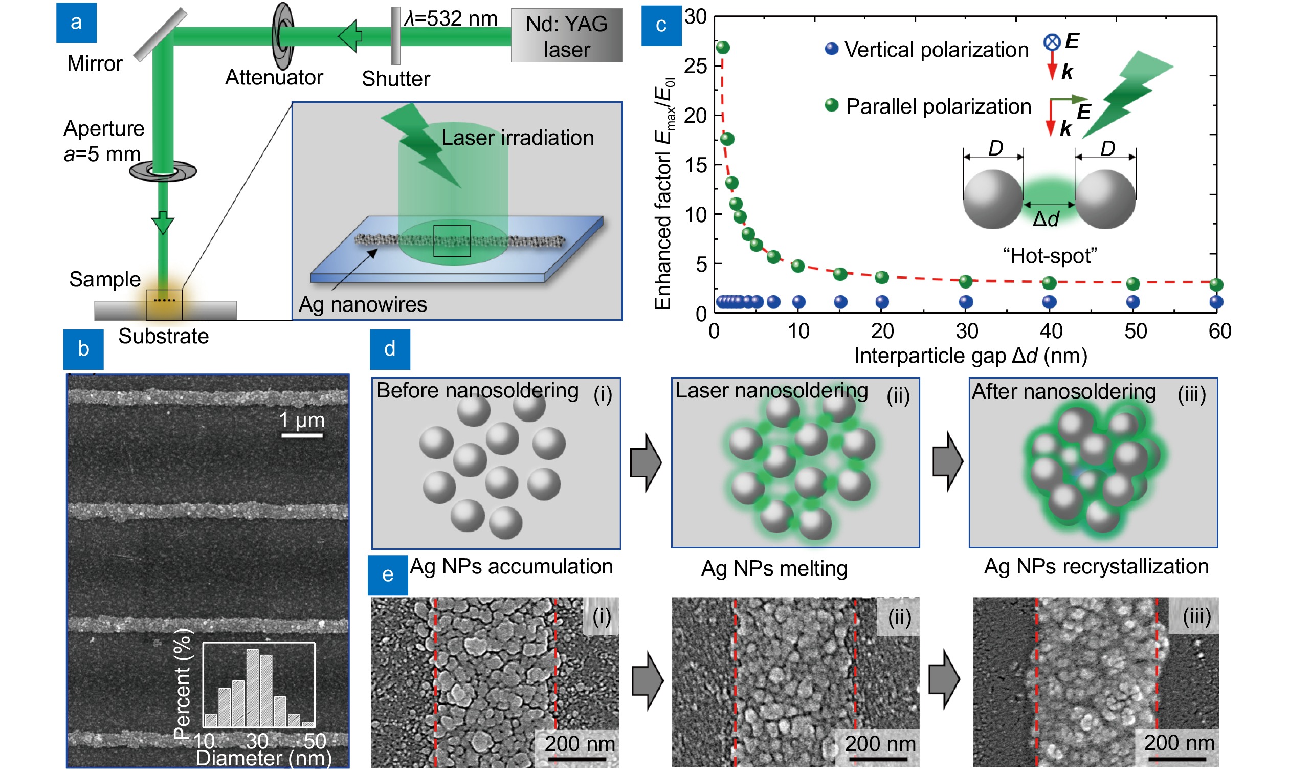
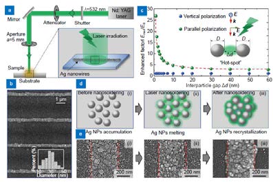
Figure 1.
(a) Schematic of experimental system for PLNS. (b) Scanning electron microscope (SEM) image of Ag NWs with inset showing the size distribution of Ag NPs in Ag NWs. (c) Plasmon-enhanced electric field as a function of interparticle gap for light polarization direction parallel and vertical to the interparticle axis. (d) Schematic illustration of PLNS with increasing laser irradiation time. (e) SEM images of the morphological changes of Ag NWs in PLNS process.
-
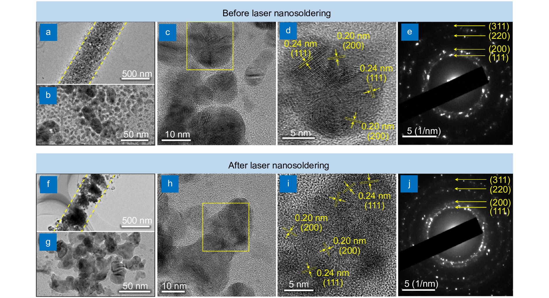
Figure 2.
TEM images of Ag NWs for overall (a), local (b) and magnified (c) topographies before the laser illumination. (d) Typical HRTEM images and (e) SAED patterns of Ag NPs before the laser illumination. TEM images of Ag NWs for overall (f), local (g) and magnified (h) topographies after the illumination. (i) Typical HRTEM images and (j) SAED pattern of Ag NPs after laser illumination for 15 min.
-
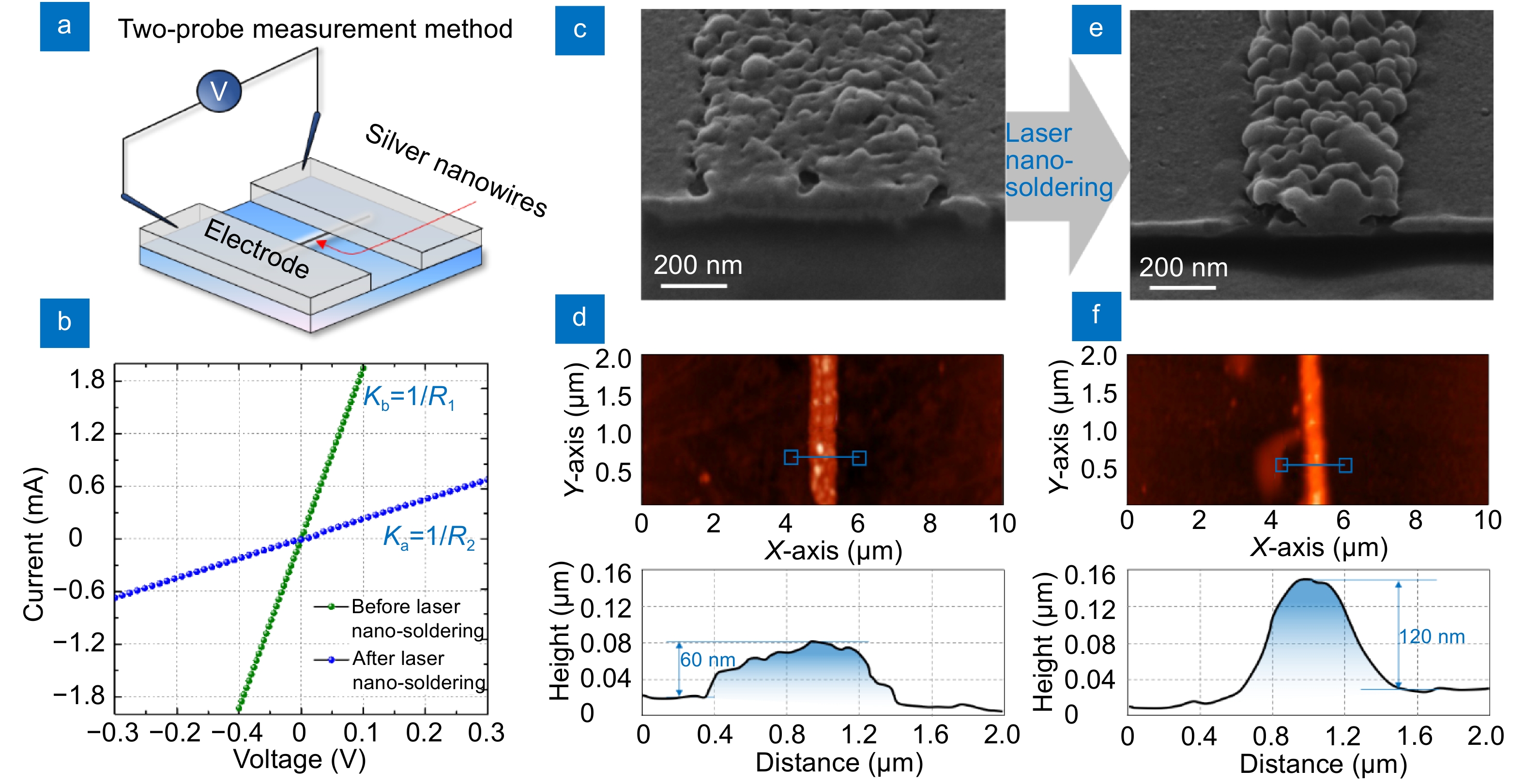
Figure 3.
(a) Schematic of two-probe measurement method. (b) I-V curve of the fabricated Ag NWs before and after the laser nanosoldering. (c, f) Morphology of Ag NWs cut by focus ion beam. (d, g) AFM images and the height profile of the Ag NWs before and after the laser nanosoldering.
-
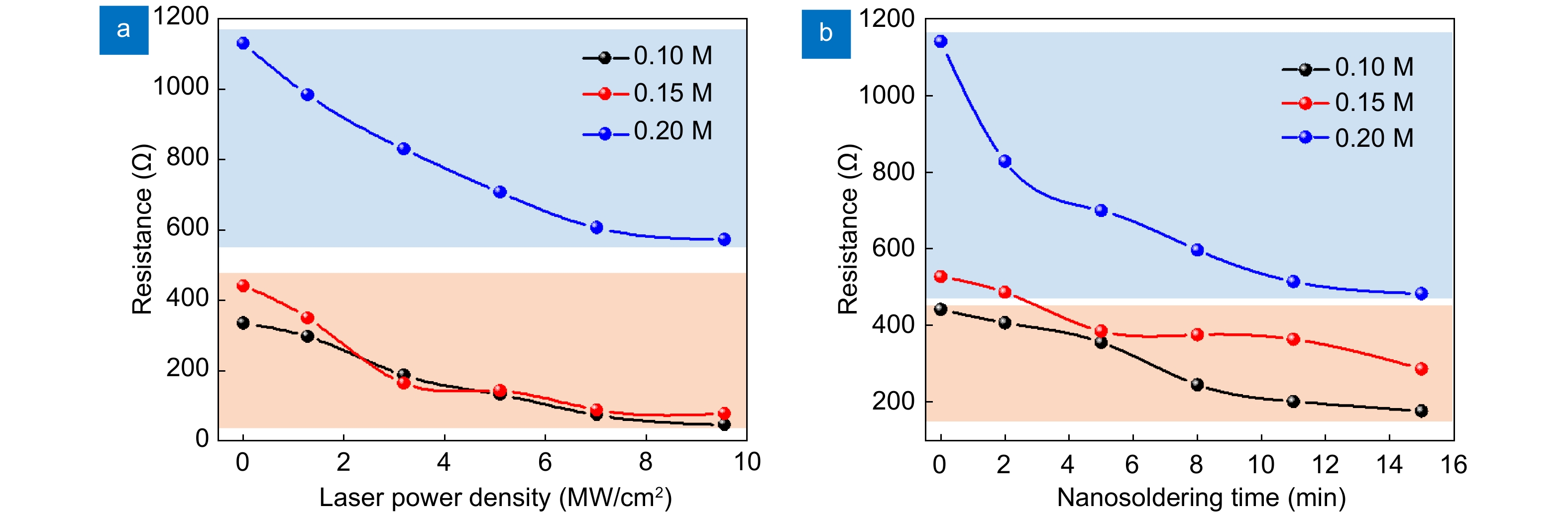
Figure 4.
(a) Measured resistance of the Ag NWs electrodes as a function of the laser nanosoldering power density with the laser nanosoldering time of 11 min. (b) Measured resistance of the Ag NWs electrodes as a function of the laser nanosoldering time with laser nanosoldering power density of 7.01 MW/cm2.
-
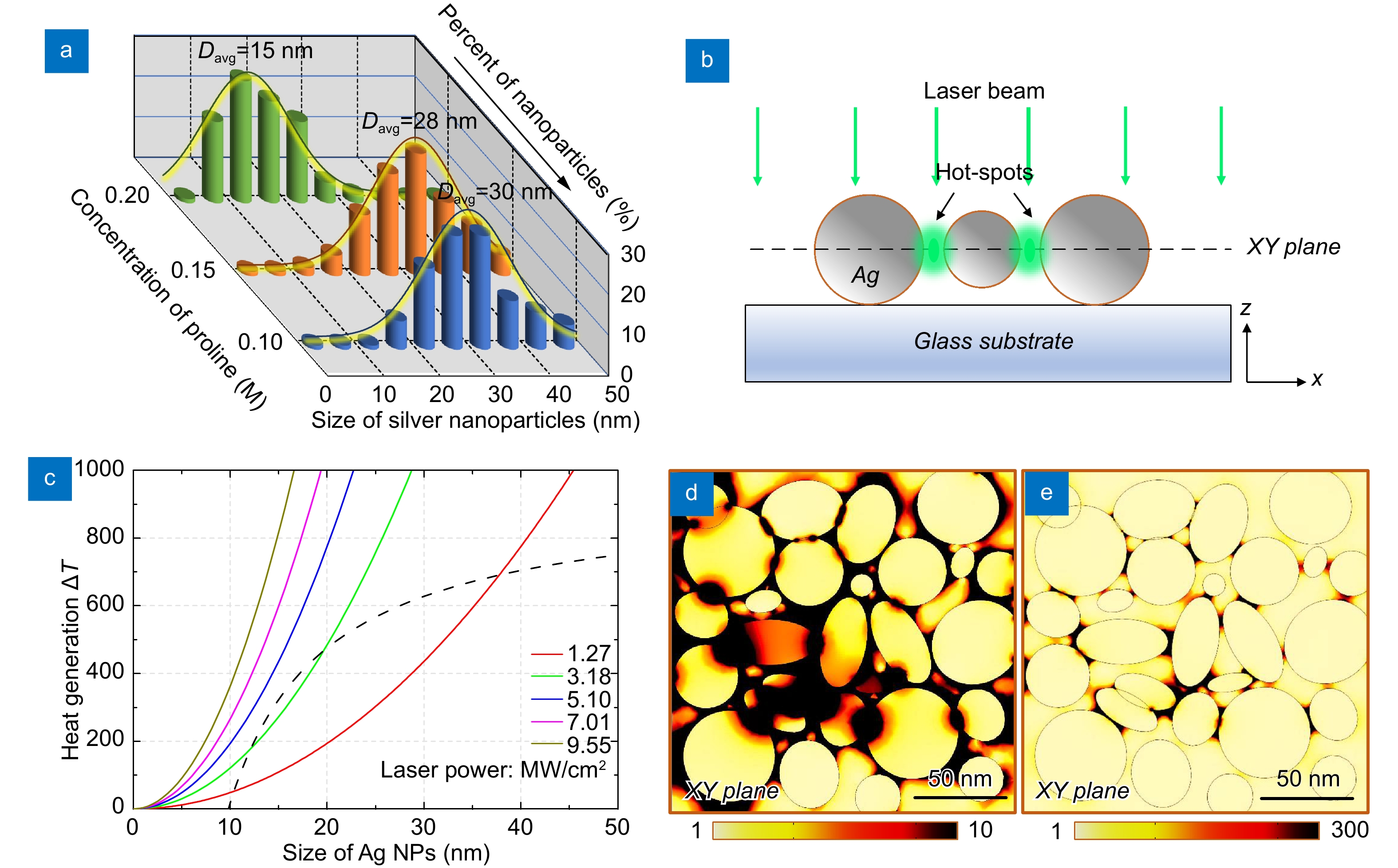
Figure 5.
(a) Size distribution of Ag NPs in the Ag NWs fabricated in the silver ion contained precursor solutions at different concentrations of surfactant. (b) Schematic of simulation setup, a planar configuration is taken as an example. (c) Calculated temperature increasing ΔT (°C) at the surface of Ag NPs as a function of Ag NPs size, considering the local light intensity increased 300 times. The black areas (hot-spots) present the simulation results of the temperature distributions when the enhanced light field intensity increases 10 (d) and 300 (e) times by using FEM method.
- Figure FIG. 1183..


