| Citation: | Lyu JB, Zhu T, Zhou Y et al. Inverse design for material anisotropy and its application for a compact X-cut TFLN on-chip wavelength demultiplexer. Opto-Electron Sci 2, 230038 (2023). doi: 10.29026/oes.2023.230038 |
Inverse design for material anisotropy and its application for a compact X-cut TFLN on-chip wavelength demultiplexer
-
Abstract
Inverse design focuses on identifying photonic structures to optimize the performance of photonic devices. Conventional scalar-based inverse design approaches are insufficient to design photonic devices of anisotropic materials such as lithium niobate (LN). To the best of our knowledge, this work proposes for the first time the inverse design method for anisotropic materials to optimize the structure of anisotropic-material based photonics devices. Specifically, the orientation dependent properties of anisotropic materials are included in the adjoint method, which provides a more precise prediction of light propagation within such materials. The proposed method is used to design ultra-compact wavelength division demultiplexers in the X-cut thin-film lithium niobate (TFLN) platform. By benchmarking the device performances of our method with those of classical scalar-based inverse design, we demonstrate that this method properly addresses the critical issue of material anisotropy in the X-cut TFLN platform. This proposed method fills the gap of inverse design of anisotropic materials based photonic devices, which finds prominent applications in TFLN platforms and other anisotropic-material based photonic integration platforms. -

-
References
[1] Koenderink AF, Alù A, Polman A. Nanophotonics: shrinking light-based technology. Science 348, 516–521 (2015). doi: 10.1126/science.1261243 [2] Liu ZC, Zhu DY, Raju L, Cai WS. Tackling photonic inverse design with machine learning. Adv Sci 8, 2002923 (2021). doi: 10.1002/advs.202002923 [3] Molesky S, Lin ZN, Piggott AY, Jin WL, Vucković J et al. Inverse design in nanophotonics. Nat Photonics 12, 659–670 (2018). doi: 10.1038/s41566-018-0246-9 [4] Callewaert F, Velev V, Kumar P, Sahakian AV, Aydin K. Inverse-designed broadband all-dielectric electromagnetic metadevices. Sci Rep 8, 1358 (2018). doi: 10.1038/s41598-018-19796-y [5] Su LG, Trivedi R, Sapra NV, Piggott AY, Vercruysse D et al. Fully-automated optimization of grating couplers. Opt Express 26, 4023–4034 (2018). doi: 10.1364/OE.26.004023 [6] Lin CH, Chen YS, Lin JT, Wu HC, Kuo HT et al. Automatic inverse design of high-performance beam-steering metasurfaces via genetic-type tree optimization. Nano Lett 21, 4981–4989 (2021). doi: 10.1021/acs.nanolett.1c00720 [7] Feichtner T, Selig O, Kiunke M, Hecht B. Evolutionary optimization of optical antennas. Phys Rev Lett 109, 127701 (2012). doi: 10.1103/PhysRevLett.109.127701 [8] Qi HX, Du ZC, Hu XY, Yang JY, Chu SS et al. High performance integrated photonic circuit based on inverse design method. Opto-Electron Adv 5, 210061 (2022). doi: 10.29026/oea.2022.210061 [9] Hughes TW, Minkov M, Williamson IAD, Fan SH. Adjoint method and inverse design for nonlinear nanophotonic devices. ACS Photonics 5, 4781–4787 (2018). doi: 10.1021/acsphotonics.8b01522 [10] Liu JC, Zhang D, Yu DQ, Ren MX, Xu JJ. Machine learning powered ellipsometry. Light Sci Appl 10, 55 (2021). doi: 10.1038/s41377-021-00482-0 [11] Paganini A, Sargheini S, Hiptmair R, Hafner C. Shape optimization of microlenses. Opt Express 23, 13099–13107 (2015). doi: 10.1364/OE.23.013099 [12] Zhu RC, Qiu TS, Wang JF, Sui S, Hao CL et al. Phase-to-pattern inverse design paradigm for fast realization of functional metasurfaces via transfer learning. Nat Commun 12, 2974 (2021). doi: 10.1038/s41467-021-23087-y [13] Jiang JQ, Fan JA. Global optimization of dielectric metasurfaces using a physics-driven neural network. Nano Lett 19, 5366–5372 (2019). doi: 10.1021/acs.nanolett.9b01857 [14] Krasikov S, Tranter A, Bogdanov A, Kivshar Y. Intelligent metaphotonics empowered by machine learning. Opto-Electron Adv 5, 210147 (2022). doi: 10.29026/oea.2022.210147 [15] Ma TG, Tobah M, Wang HZ, Guo LJ. Benchmarking deep learning-based models on nanophotonic inverse design problems. Opto-Electron Sci 1, 210012 (2022). doi: 10.29026/oes.2022.210012 [16] Zhou M, Liu DJ, Belling SW, Cheng HT, Kats MA et al. Inverse design of metasurfaces based on coupled-mode theory and adjoint optimization. ACS Photonics 8, 2265–2273 (2021). doi: 10.1021/acsphotonics.1c00100 [17] Sell D, Yang JJ, Doshay S, Yang R, Fan JA. Large-angle, multifunctional metagratings based on freeform multimode geometries. Nano Lett 17, 3752–3757 (2017). doi: 10.1021/acs.nanolett.7b01082 [18] Piggott AY, Lu J, Lagoudakis KG, Petykiewicz J, Babinec TM et al. Inverse design and demonstration of a compact and broadband on-chip wavelength demultiplexer. Nat Photonics 9, 374–377 (2015). doi: 10.1038/nphoton.2015.69 [19] Fan LJ, Mei J. Acoustic metagrating circulators: nonreciprocal, robust, and tunable manipulation with unitary efficiency. Phys Rev Appl 15, 064002 (2021). doi: 10.1103/PhysRevApplied.15.064002 [20] Sell D, Yang JJ, Wang EW, Phan T, Doshay S et al. Ultra-high-efficiency anomalous refraction with dielectric metasurfaces. ACS Photonics 5, 2402–2407 (2018). doi: 10.1021/acsphotonics.8b00183 [21] Dai DX. Advanced passive silicon photonic devices with asymmetric waveguide structures. Proc IEEE 106, 2117–2143 (2018). doi: 10.1109/JPROC.2018.2822787 [22] Bayati E, Pestourie R, Colburn S, Lin ZN, Johnson SG et al. Inverse designed metalenses with extended depth of focus. ACS Photonics 7, 873–878 (2020). doi: 10.1021/acsphotonics.9b01703 [23] Ramirez JM, Elfaiki H, Verolet T, Besancon C, Gallet A et al. III-V-on-silicon integration: from hybrid devices to heterogeneous photonic integrated circuits. IEEE J Sel Top Quantum Electron 26, 6100213 (2020). [24] Zhu D, Shao LB, Yu MJ, Cheng R, Desiatov B et al. Integrated photonics on thin-film lithium niobate. Adv Opt Photonics 13, 242–352 (2021). doi: 10.1364/AOP.411024 [25] Shang CF, Yang JW, Hammond AM, Chen ZX, Chen M et al. Inverse-designed lithium niobate nanophotonics. ACS Photonics 10, 1019–1026 (2023). doi: 10.3390/photonics10091019 [26] Xie YJ, Nie MM, Huang SW. Inverse-designed broadband low-loss grating coupler on thick lithium-niobate-on-insulator platform. arXiv: 2309.12976 (2023). https://doi.org/10.48550/arXiv.2309.12976 [27] Xu Q, Liu JM, Zhang DL, Hua PR. Ultra-compact lithium niobate power splitters designed by an intelligent algorithm. Opt Laser Technol 160, 109057 (2023). doi: 10.1016/j.optlastec.2022.109057 [28] Chen GY, Ng JD, Lin HL, Zhang G, Gong X et al. Design and fabrication of high-performance multimode interferometer in lithium niobate thin film. Opt Express 29, 15689–15698 (2021). doi: 10.1364/OE.419255 [29] Zhang L, Zhang L, Fu X, Yang L. Compact, broadband and low-loss polarization beam splitter on lithium-niobate-on-insulator using a silicon nanowire assisted waveguide. IEEE Photonics J 12, 6601906 (2020). [30] Kar A, Bahadori M, Gong SB, Goddard LL. Realization of alignment-tolerant grating couplers for z-cut thin-film lithium niobate. Opt Express 27, 15856–15867 (2019). doi: 10.1364/OE.27.015856 [31] Tu HL, Zhang YD, Guo WH. Arrayed waveguide grating based on z-cut lithium niobate platform. In 2023 Opto-Electronics and Communications Conference (OECC) 1–3 (IEEE, 2023);http://doi.org/10.1109/OECC56963.2023.10209708. [32] Gong Z, Liu XW, Xu YT, Xu MR, Surya JB et al. Soliton microcomb generation at 2 μm in z-cut lithium niobate microring resonators. Opt Lett 44, 3182–3185 (2019). doi: 10.1364/OL.44.003182 [33] Chen GY, Lin HL, Ng JD, Danner AJ. Integrated thermally tuned Mach-Zehnder interferometer in z-cut lithium niobate thin film. IEEE Photonics Technol Lett 33, 664–667 (2021). doi: 10.1109/LPT.2021.3086850 [34] Chen GY, Lin HL, Ng JD, Danner AJ. Integrated electro-optic modulator in z-cut lithium niobate thin film with vertical structure. IEEE Photonics Technol Lett 33, 1285–1288 (2021). doi: 10.1109/LPT.2021.3114993 [35] Zhao WK, Liu RR, Zhu MY, Guo ZH, He JH et al. High-performance mode-multiplexing device with anisotropic lithium-niobate-on-insulator waveguides. Laser Photonics Rev 17, 2200774 (2023). doi: 10.1002/lpor.202200774 [36] Zheng XX, Lin ZX, Huang QS, He SL. Elimination of the fundamental mode hybridization on an x-cut lithium-niobate-on-insulator by using a densely packed bent waveguide array. Appl Opt 62, 5765–5771 (2023). doi: 10.1364/AO.495166 [37] Chen GX, Ruan ZL, Wang Z, Huang PC, Guo CJ et al. Four-channel CWDM device on a thin-film lithium niobate platform using an angled multimode interferometer structure. Photonics Res 10, 8–13 (2022). [38] Pan BC, Tan Y, Chen PX, Liu L, Shi YC et al. Compact racetrack resonator on LiNbO3. J Lightwave Technol 39, 1770–1776 (2021). doi: 10.1109/JLT.2020.3040387 [39] Liu HX, Pan BC, Huang YS, He JH, Zhang M et al. Ultra-compact lithium niobate photonic chip for high-capacity and energy-efficient wavelength-division-multiplexing transmitters. Light Adv Manuf 4, 133–142 (2023). [40] Tan HY, Wang J, Ke W, Zhang X, Zhao ZK et al. C-Band optical 90-degree hybrid using thin film lithium niobate. Opt Lett 48, 1946–1949 (2023). doi: 10.1364/OL.480380 [41] Liu XY, Gao SQ, Zhang C, Pan Y, Ma R et al. Ultra-broadband and low-loss edge coupler for highly efficient second harmonic generation in thin-film lithium niobate. Adv Photonics Nexus 1, 016001 (2022). [42] Xu MY, Zhu YT, Pittalà F, Tang J, He MB et al. Dual-polarization thin-film lithium niobate in-phase quadrature modulators for terabit-per-second transmission. Optica 9, 61–62 (2022). doi: 10.1364/OPTICA.449691 [43] Halir R, Cheben P, Luque-González JM, Sarmiento-Merenguel JD, Schmid JH et al. Ultra-broadband nanophotonic beamsplitter using an anisotropic sub-wavelength metamaterial. Laser Photonics Rev 10, 1039–1046 (2016). doi: 10.1002/lpor.201600213 [44] Zhuang RJ, He JZ, Qi YF, Li Y. High-Q thin-film lithium niobate microrings fabricated with wet etching. Adv Mater 35, 2208113 (2023). doi: 10.1002/adma.202208113 [45] Sun DH, Zhang YW, Wang DZ, Song W, Liu XY et al. Microstructure and domain engineering of lithium niobate crystal films for integrated photonic applications. Light Sci Appl 9, 197 (2020). doi: 10.1038/s41377-020-00434-0 [46] Rao A, Patil A, Rabiei P, Honardoost A, Desalvo R et al. High-performance and linear thin-film lithium niobate Mach–Zehnder modulators on silicon up to 50 GHz. Opt Lett 41, 5700–5703 (2016). doi: 10.1364/OL.41.005700 [47] He MB, Xu MY, Ren YX, Jian J, Ruan ZL et al. High-performance hybrid silicon and lithium niobate Mach–Zehnder modulators for 100 Gbit s−1 and beyond. Nat Photonics 13, 359–364 (2019). doi: 10.1038/s41566-019-0378-6 [48] Chen L, Xu Q, Wood MG, Reano RM. Hybrid silicon and lithium niobate electro-optical ring modulator. Optica 1, 112–118 (2014). doi: 10.1364/OPTICA.1.000112 [49] Weigel PO, Zhao J, Fang K, Al-Rubaye H, Trotter D et al. Bonded thin film lithium niobate modulator on a silicon photonics platform exceeding 100 GHz 3-dB electrical modulation bandwidth. Opt Express 26, 23728–23739 (2018). doi: 10.1364/OE.26.023728 [50] Jensen JS, Sigmund O. Topology optimization for nano-photonics. Laser Photonics Rev 5, 308–321 (2011). doi: 10.1002/lpor.201000014 [51] Lin Z, Liu V, Pestourie R, Johnson SG. Topology optimization of freeform large-area metasurfaces. Opt Express 27, 15765–15775 (2019). doi: 10.1364/OE.27.015765 [52] Wang Q, Chumak AV, Pirro P. Inverse-design magnonic devices. Nat Commun 12, 2636 (2021). doi: 10.1038/s41467-021-22897-4 [53] Boes A, Corcoran B, Chang L, Bowers J, Mitchell A. Status and potential of lithium niobate on insulator (LNOI) for photonic integrated circuits. Laser Photonics Rev 12, 1700256 (2018). doi: 10.1002/lpor.201700256 [54] Lee D, So S, Hu GW, Kim M, Badloe T et al. Hyperbolic metamaterials: fusing artificial structures to natural 2D materials. eLight 2, 1 (2022). doi: 10.1186/s43593-021-00008-6 [55] Dai ZG, Hu GW, Si GY, Ou QD, Zhang Q et al. Edge-oriented and steerable hyperbolic polaritons in anisotropic van der Waals nanocavities. Nat Commun 11, 6086 (2020). doi: 10.1038/s41467-020-19913-4 [56] Lalau-Keraly CM, Bhargava S, Miller OD, Yablonovitch E. Adjoint shape optimization applied to electromagnetic design. Opt Express 21, 21693–21701 (2013). doi: 10.1364/OE.21.021693 -
Supplementary Information
Supplementary information for Inverse design for material anisotropy and its application for a compact X-cut TFLN on-chip wavelength demultiplexer 
-
Access History

Article Metrics
-
Figure 1.
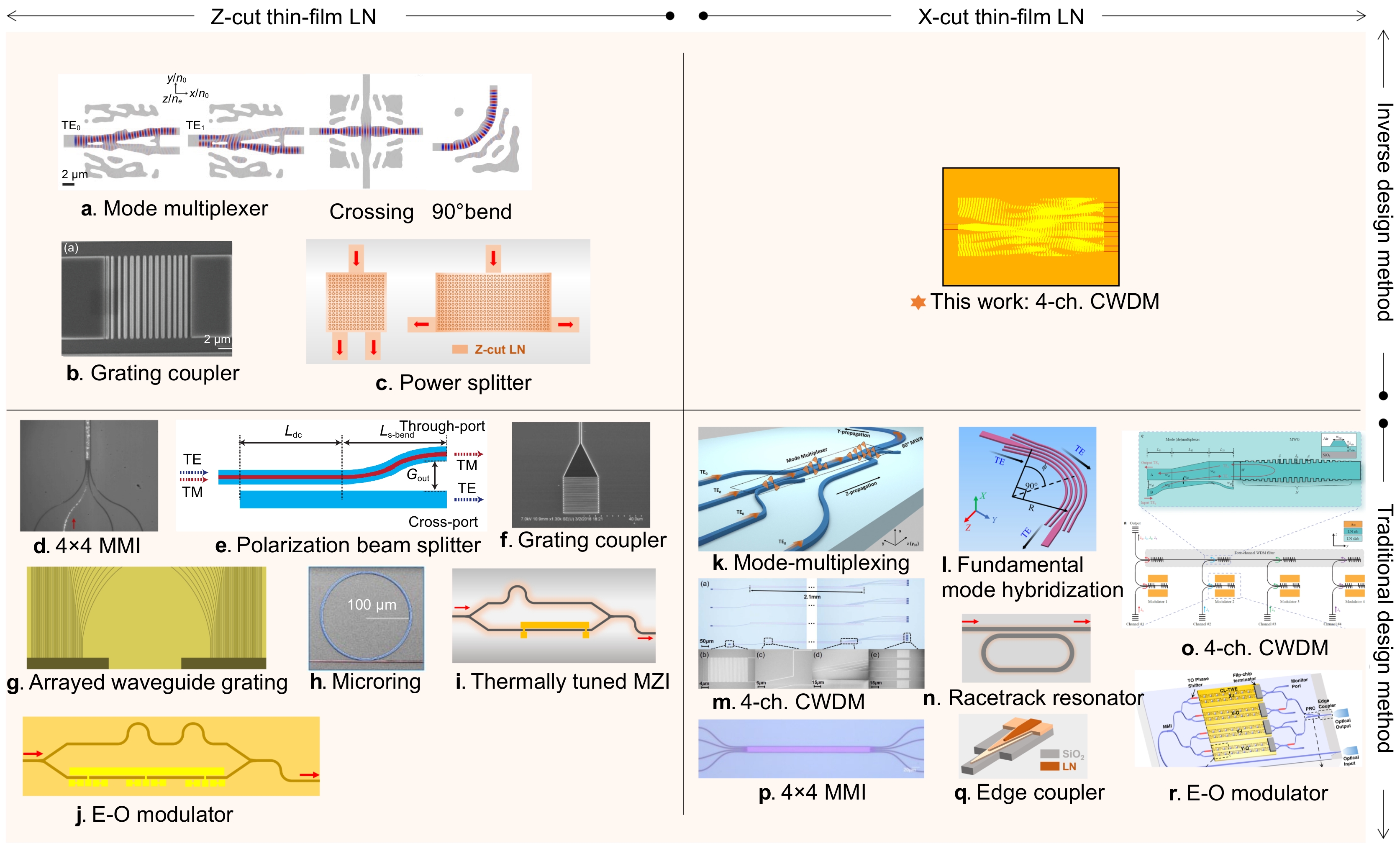
A four-quadrant diagram of photonics devices based on TFLN. (a) A spatial-mode multiplexer, a waveguide crossing, and a compact waveguide bend using a 3D gradient-based inverse-design method25. (b) A grating coupler using particle swarm optimization method26. (c) A power splitter using Direct binary search method27. (d) A 4×4 multimode interference (MMI)28. (e) A polarization beam splitter29. (f) An alignment-tolerant grating coupler30. (g) An arrayed waveguide grating31. (h) A microring resonator for soliton microcomb generation32. (i) A tunable Mach-Zehnder interferometer (MZI)33. (j) An integrated electro-optic modulator34. (k) A mode-multiplexing device35. (l) A fundamental mode hybridization36. (m) A 4 channel CWDM device37. (n) A compact racetrack resonator38. (o) A lithium niobate photonic chip for wavelength-division-multiplexing transmitters39. (p) A 4×4 MMI for C-band optical 90-degree hybrid40. (q) An ultra-broadband and low-loss edge coupler41. (r) A dual-polarization TFLN in-phase quadrature modulators42. Figure reproduced with permission from: (a) ref.25, Copyright © 2023 American Chemical Society; (b) ref.26, under a Creative Commons Attribution 4.0 International License; (d) ref.28, Copyright © 2021 Optica Publishing Group; (e) ref.29, under a Creative Commons Attribution 4.0 International License; (f) ref.30, Copyright © 2019 Optica Publishing Group; (h) ref.32, Copyright © 2019 Optica Publishing Group; (k) ref.35, Copyright © 2023 John Wiley and Sons; (l) ref.36, Copyright © 2023 Optica Publishing Group; (m) ref.37, Copyright © 2022 Chinese Laser Press; (o) ref.39, under a Creative Commons Attribution 4.0 International License; (p) ref.40, Copyright © 2023 Optica Publishing Group; (r) ref.42, Copyright © 2022 Optica Publishing Group.
-
Figure 2.
(a) Schematic diagram of the three-dimensional structure of X-cut LN waveguide. (b) Schematic diagram of refractive index ellipsoid. (c) Schematic diagram of X-cut LN and Z-cut LN.
-
Figure 3.
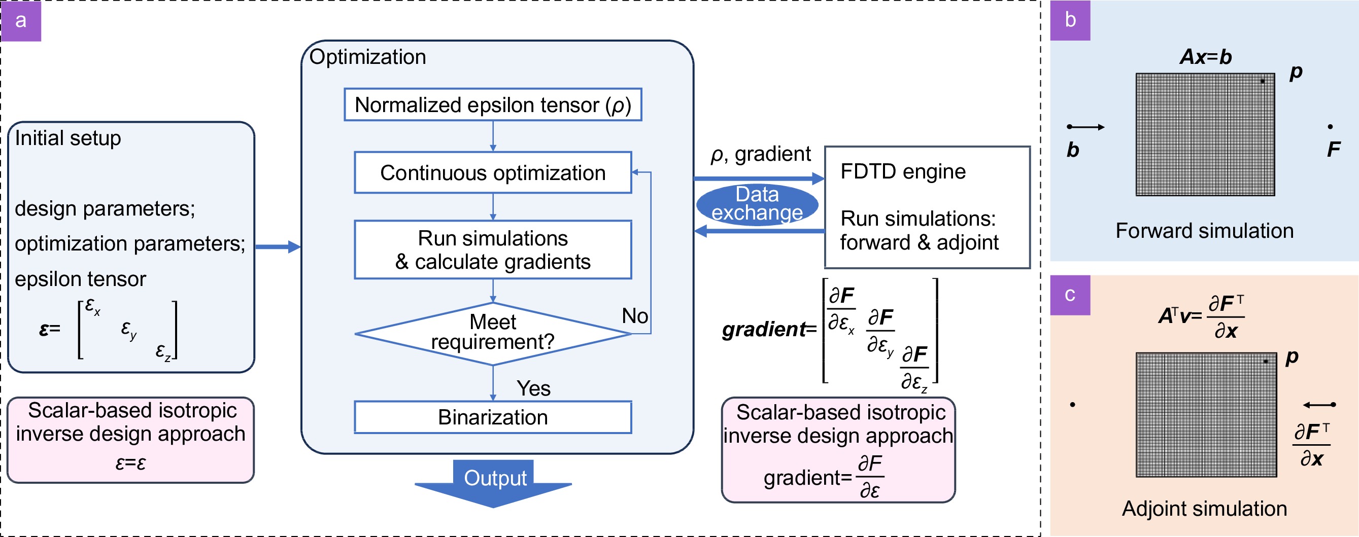
(a) Workflow of the inverse design method for anisotropic materials with the dielectric constant tensor. (b) Forward simulation of a linear system, b is a point source, F is the objective function at the measuring point, and p is the spatial distribution of the dielectric constant. (c) Adjoint simulation of a linear system, the point source given by ∂FT/∂x is located at the measuring point.
-
Figure 4.
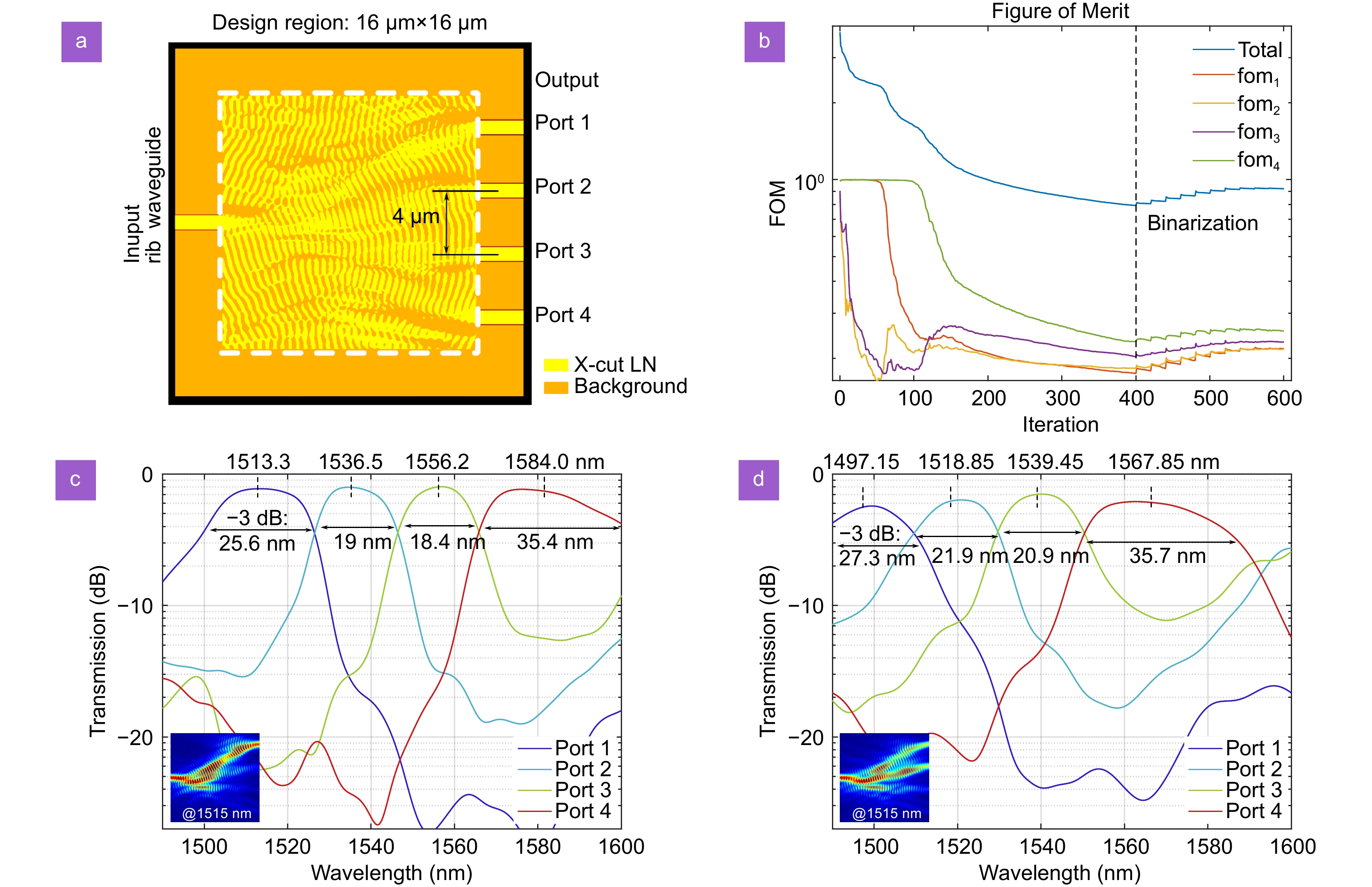
(a) Schematic of the inverse design of a thin-film LN four-channel wavelength division demultiplexer device. (b) The iterative process of FOM during the inverse design process, including the FOM for the four ports and the total FOM (blue line) of the device. (c) Spectral response of four output ports verified in FDTD simulation of a structure designed by inverse design using isotropic materials. Inset is the electric field distribution within the design region while the center wavelength of the input optical signal is 1515 nm. (d) Spectral response of four output ports verified in FDTD simulation of the same structure after setting the material of the structure to the tensor form of X-cut LN. Inset is the electric field distribution within the design region while the center wavelength of the input optical signal is 1515 nm.
-
Figure 5.
(a) The iterative process of FOM during the inverse design process using anisotropic materials, including the FOM for the four ports and the total FOM (blue) of the device. (b) Spectral response of four output ports verified in FDTD simulation of a structure designed by inverse design using anisotropic materials. (c) The electric field distribution within the design region while the center wavelengths of the input optical signal are 1515 nm, 1535 nm, 1555 nm, and 1575 nm, respectively. (d) The device structure designed using the scalar-based and the proposed inverse design methods for anisotropic materials, respectively.
-
Figure 6.
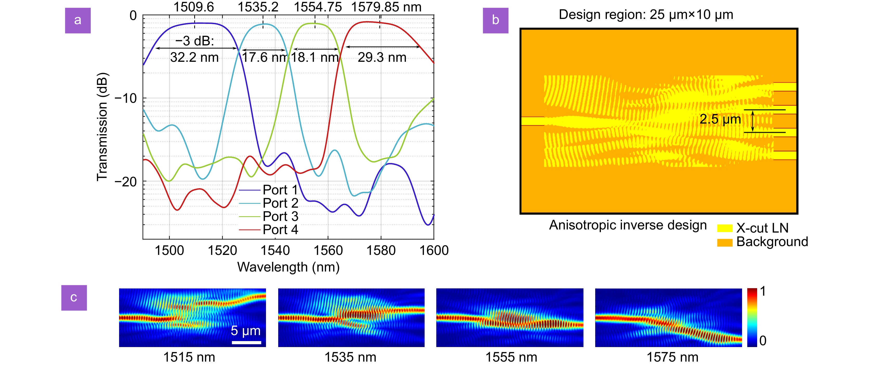
(a) Spectral response of four output ports verified in FDTD simulation. (b) The device structure with an initial design region of 25 µm×10 µm. (c) Electric field distributions within the design region for center wavelengths of the input optical signal at 1515 nm, 1535 nm, 1555 nm, and 1575 nm, respectively.

 E-mail Alert
 RSS
RSS

 DownLoad:

