
 E-mail Alert
 RSS
RSS
| Citation: |
Jia LM, Cheng L, Zheng W. 8-nm narrowband photodetection in diamonds. Opto-Electron Sci 2, 230010 (2023). doi: 10.29026/oes.2023.230010

|
-
Abstract
Spectrally-selective photodetection plays a crucial role in various applications, including target imaging and environmental monitoring. Traditional deep-ultraviolet (DUV) narrowband photodetection systems consist of broadband photodetectors and filters, which complicates the architecture and constrains imaging quality. Here, we introduce an electronic-grade diamond single-crystal photodetector exhibiting an exceptionally narrow spectral response in the DUV range with a full width at half maximum of 8 nm. By examining diamond photodetectors with varying dislocation densities, we propose that mitigating the defect-induced trapping effect to achieve charge collection narrowing, assisted by free exciton radiative recombination, is an effective strategy for narrowband photodetection. The superior performance of this device is evidenced through the imaging of DUV light sources, showcasing its capability to differentiate between distinct light sources and monitor human-safe sterilization systems. Our findings underscore the promising potential applications of electronic-grade diamond in narrowband photodetection and offer a valuable technique for identifying electronic-grade diamond. -

-
References
[1] Konstantatos G, Sargent EH. Nanostructured materials for photon detection. Nat Nanotechnol 5, 391–400 (2010). doi: 10.1038/nnano.2010.78 [2] de Arquer FPG, Armin A, Meredith P, Sargent EH. Solution-processed semiconductors for next-generation photodetectors. Nat Rev Mater 2, 16100 (2017). doi: 10.1038/natrevmats.2016.100 [3] Lee W, Liu Y, Lee Y, Sharma BK, Shinde SM et al. Two-dimensional materials in functional three-dimensional architectures with applications in photodetection and imaging. Nat Commun 9, 1417 (2018). doi: 10.1038/s41467-018-03870-0 [4] Lukac R. Single-sensor imaging in consumer digital cameras: a survey of recent advances and future directions. J Real-Time Image Proc 1, 45–52 (2006). doi: 10.1007/s11554-006-0003-z [5] Dai Y, Jia KP, Zhu GH, Li H, Fei Y et al. All-fiber device for single-photon detection. PhotoniX 4, 7 (2023). doi: 10.1186/s43074-023-00085-5 [6] Armin A, Hambsch M, Kim IK, Burn PL, Meredith P et al. Thick junction broadband organic photodiodes. Laser Photonics Rev 8, 924–932 (2014). doi: 10.1002/lpor.201400081 [7] Zou HY, Li XG, Peng WB, Wu WZ, Yu RM et al. Piezo-phototronic effect on selective electron or hole transport through depletion region of vis–NIR broadband photodiode. Adv Mater 29, 1701412 (2017). doi: 10.1002/adma.201701412 [8] Zhao ZJ, Xu CY, Niu LB, Zhang XL, Zhang FJ. Recent progress on broadband organic photodetectors and their applications. Laser Photonics Rev 14, 2000262 (2020). doi: 10.1002/lpor.202000262 [9] Li ZW, Yang W, Huang M, Yang X, Zhu CG et al. Light-triggered interfacial charge transfer and enhanced photodetection in CdSe/ZnS quantum dots/MoS2 mixed-dimensional phototransistors. Opto-Electron Adv 4, 210017 (2021). doi: 10.29026/oea.2021.210017 [10] Yan SQ, Zuo Y, Xiao SS, Oxenløwe LK, Ding YH. Graphene photodetector employing double slot structure with enhanced responsivity and large bandwidth. Opto-Electron Adv 5, 210159 (2022). doi: 10.29026/oea.2022.210159 [11] Armin A, Jansen-van Vuuren RD, Kopidakis N, Burn PL, Meredith P. Narrowband light detection via internal quantum efficiency manipulation of organic photodiodes. Nat Commun 6, 6343 (2015). doi: 10.1038/ncomms7343 [12] Lin QQ, Armin A, Burn PL, Meredith P. Filterless narrowband visible photodetectors. Nat Photonics 9, 687–694 (2015). doi: 10.1038/nphoton.2015.175 [13] Juntunen MA, Heinonen J, Vähänissi V, Repo P, Valluru D et al. Near-unity quantum efficiency of broadband black silicon photodiodes with an induced junction. Nat Photonics 10, 777–781 (2016). doi: 10.1038/nphoton.2016.226 [14] Gao Y, Cansizoglu H, Polat KG, Ghandiparsi S, Kaya A et al. Photon-trapping microstructures enable high-speed high-efficiency silicon photodiodes. Nat Photonics 11, 301–308 (2017). doi: 10.1038/nphoton.2017.37 [15] Wang BH, Mu JF. High-speed Si-Ge avalanche photodiodes. PhotoniX 3, 8 (2022). doi: 10.1186/s43074-022-00052-6 [16] Zheng ZY, Luo Q, Xu KK et al. All-silicon PIN photodetector based on black silicon microstructure. Opto-Electron Eng 48, 200364 (2021). doi: 10.12086/oee.2021.200364 [17] Xu T, Wu YK, Luo XG, Guo LJ. Plasmonic nanoresonators for high-resolution colour filtering and spectral imaging. Nat Commun 1, 59 (2010). doi: 10.1038/ncomms1058 [18] Yokogawa S, Burgos SP, Atwater HA. Plasmonic color filters for CMOS image sensor applications. Nano Lett 12, 4349–4354 (2012). doi: 10.1021/nl302110z [19] Kim JH, Liess A, Stolte M, Krause AM, Stepanenko V et al. An efficient narrowband near-infrared at 1040 nm organic photodetector realized by intermolecular charge transfer mediated coupling based on a squaraine dye. Adv Mater 33, 2100582 (2021). doi: 10.1002/adma.202100582 [20] Fang YJ, Dong QF, Shao YC, Yuan YB, Huang JS. Highly narrowband perovskite single-crystal photodetectors enabled by surface-charge recombination. Nat Photonics 9, 679–686 (2015). doi: 10.1038/nphoton.2015.156 [21] Hou YC, Wu CC, Huang X, Yang D, Ye T et al. Self-powered Red/UV narrowband photodetector by unbalanced charge carrier transport strategy. Adv Funct Mater 31, 2007016 (2021). doi: 10.1002/adfm.202007016 [22] Xie C, Lu XT, Tong XW, Zhang ZX, Liang FX et al. Recent progress in solar-blind deep-ultraviolet photodetectors based on inorganic ultrawide bandgap semiconductors. Adv Funct Mater 29, 1806006 (2019). doi: 10.1002/adfm.201806006 [23] Jia LM, Zheng W, Huang F. Vacuum-ultraviolet photodetectors. PhotoniX 1, 22 (2020). doi: 10.1186/s43074-020-00022-w [24] Zheng W, Jia LM, Huang F. Vacuum-ultraviolet photon detections. iScience 23, 101145 (2020). doi: 10.1016/j.isci.2020.101145 [25] Liu C, Eschen W, Loetgering L, Penagos Molina DS, Klas R et al. Visualizing the ultra-structure of microorganisms using table-top extreme ultraviolet imaging. PhotoniX 4, 6 (2023). doi: 10.1186/s43074-023-00084-6 [26] Wilks J, Wilks E. Properties and Applications of Diamond (Butterworth-Heinemann, Oxford, 1991). [27] Lu YJ, Lin CN, Shan CX. Optoelectronic diamond: growth, properties, and photodetection applications. Adv Opt Mater 6, 1800359 (2018). doi: 10.1002/adom.201800359 [28] Liao MY. Progress in semiconductor diamond photodetectors and MEMS sensors. Funct Diamond 1, 29–46 (2021). doi: 10.1080/26941112.2021.1877019 [29] Neamen DA. Semiconductor Physics and Devices: Basic Principles (McGraw-Hill, Boston, 2003). [30] Kawarada H, Matsuyama H, Yokota Y, Sogi T, Yamaguchi A et al. Excitonic recombination radiation in undoped and boron-doped chemical-vapor-deposited diamonds. Phys Rev B 47, 3633–3637 (1993). doi: 10.1103/PhysRevB.47.3633 [31] Nebel CE. Electronic properties of CVD diamond. Semicond Sci Technol 18, S1–S11 (2003). doi: 10.1088/0268-1242/18/3/301 [32] Moram MA, Vickers ME. X-ray diffraction of III-nitrides. Rep Prog Phys 72, 036502 (2009). doi: 10.1088/0034-4885/72/3/036502 [33] Hull D, Bacon DJ. Introduction to Dislocations 4th ed (Butterworth-Heinemann, Oxford, 2001). [34] Solin SA, Ramdas AK. Raman spectrum of diamond. Phys Rev B 1, 1687–1698 (1970). doi: 10.1103/PhysRevB.1.1687 [35] Saidaminov MI, Haque A, Savoie M, Abdelhady AL, Cho N et al. Perovskite photodetectors operating in both narrowband and broadband regimes. Adv Mater 28, 8144–8149 (2016). doi: 10.1002/adma.201601235 [36] Wang J, Xiao S, Qian W, Zhang K, Yu J et al. Self-driven perovskite narrowband photodetectors with tunable spectral responses. Adv Mater 33, 2005557 (2021). doi: 10.1002/adma.202005557 [37] Li JZ, Wang J, Ma JQ, Shen HZ, Li L et al. Self-trapped state enabled filterless narrowband photodetections in 2D layered perovskite single crystals. Nat Commun 10, 806 (2019). doi: 10.1038/s41467-019-08768-z [38] Li Y, Shi ZF, Liang WQ, Wang LT, Li S et al. Highly stable and spectrum-selective ultraviolet photodetectors based on lead-free copper-based perovskites. Mater Horiz 7, 530–540 (2020). doi: 10.1039/C9MH01371G [39] Cicek E, McClintock R, Cho CY, Rahnema B, Razeghi M. AlxGa1-xN-based back-illuminated solar-blind photodetectors with external quantum efficiency of 89%. Appl Phys Lett 103, 191108 (2013). doi: 10.1063/1.4829065 [40] Seeger K. Semiconductor Physics: An Introduction 9th ed (Springer Science, New York, 2013). [41] Koizumi S, Nebel C, Nesladek M. Physics and Applications of CVD Diamond (John Wiley & Sons, Weinheim, 2008). [42] Clark CD, Dean PJ, Harris PV. Intrinsic edge absorption in diamond. Proc Roy Soc A Math Phys Eng Sci 277, 312–329 (1964). doi: 10.1098/rspa.1964.0025 [43] Konishi K, Naka N. Phonon-assisted excitonic absorption in diamond. Phys Rev B 104, 125204 (2021). doi: 10.1103/PhysRevB.104.125204 [44] Cheng L, Zheng W, Zhu YM, Huang F, Wang HK et al. Anomalous blue shift of exciton luminescence in diamond. Nano Lett 22, 1604–1608 (2022). doi: 10.1021/acs.nanolett.1c04519 [45] Cheng L, Zhu SQ, Ouyang XP, Zheng W. Bandgap evolution of diamond. Diamond Relat Mater 132, 109638 (2023). doi: 10.1016/j.diamond.2022.109638 [46] Okushi H, Watanabe H, Kanno S. Characteristics of excitonic emission in diamond. Phys Status Solidi 202, 2051–2058 (2005). doi: 10.1002/pssa.200561922 [47] Swinehart DF. The beer-lambert law. J Chem Educ 39, 333 (1962). doi: 10.1021/ed039p333 [48] Shen XC. Semiconductor Spectra and Optical Properties (Science Press, Beijing, 1992). [49] Konishi K, Akimoto I, Isberg J, Naka N. Diffusion-related lifetime and quantum efficiency of excitons in diamond. Phys Rev B 102, 195204 (2020). doi: 10.1103/PhysRevB.102.195204 [50] Walker J. Optical absorption and luminescence in diamond. Rep Prog Phys 42, 1605–1659 (1979). doi: 10.1088/0034-4885/42/10/001 [51] Guo FW, Yang B, Yuan YB, Xiao ZG, Dong QF et al. A nanocomposite ultraviolet photodetector based on interfacial trap-controlled charge injection. Nat Nanotechnol 7, 798–802 (2012). doi: 10.1038/nnano.2012.187 [52] Fox BA, Hartsell ML, Malta DM, Wynands HA, Kao CT et al. Diamond devices and electrical properties. Diamond Relat Mater 4, 622–627 (1995). doi: 10.1016/0925-9635(94)05245-X [53] Buonanno M, Ponnaiya B, Welch D, Stanislauskas M, Randers-Pehrson G et al. Germicidal efficacy and mammalian skin safety of 222-nm UV light. Radiat Res 187, 493–501 (2017). doi: 10.1667/RR0010CC.1 -
Supplementary Information
Supplementary information for 8-nm narrowband photodetection in diamonds 
-
Access History

Figures(5)
Tables(1)
Article Metrics

Export File
Citation
Jia LM, Cheng L, Zheng W. 8-nm narrowband photodetection in diamonds. Opto-Electron Sci 2, 230010 (2023). doi: 10.29026/oes.2023.230010
Format
Content
 DownLoad:


-
Figure 1.
Device structure and narrowband photodetection of electronic-grade diamond A-based photodetectors. (a) X-ray rocking curves of (111) and (004) planes of diamond A. Insets are ϕ-scans of the (111) plane at different χ (50°–60°). (b) Raman spectrum of diamond A. (c) Schematic diagram of the device structure. (d) EQE spectra of Device 1 and Device 2 based on diamond A, where extremely narrow EQE peaks have been shown. Insets are corresponding optical photographs and responsivity spectra with photon energy as abscissa. (e) The performance of typical narrowband photodetectors over the entire spectral range with the diamond device showing the shortest detection wavelength and narrowest EQE peak.
-
Figure 2.
Narrowband photodetection mechanism based on diamond A. (a) Schematic diagram of main physical processes occurring in diamond A under photoexcitation. (b) Absorption spectrum of diamond A. The inset shows a schematic diagram of absorption process and a differential spectrum of absorption coefficient. (c) PL spectrum of diamond A under 193 nm pulse excitation. (d) and (e) Spatial distribution of photoexcited excess carrier generation rate
$ G $ -
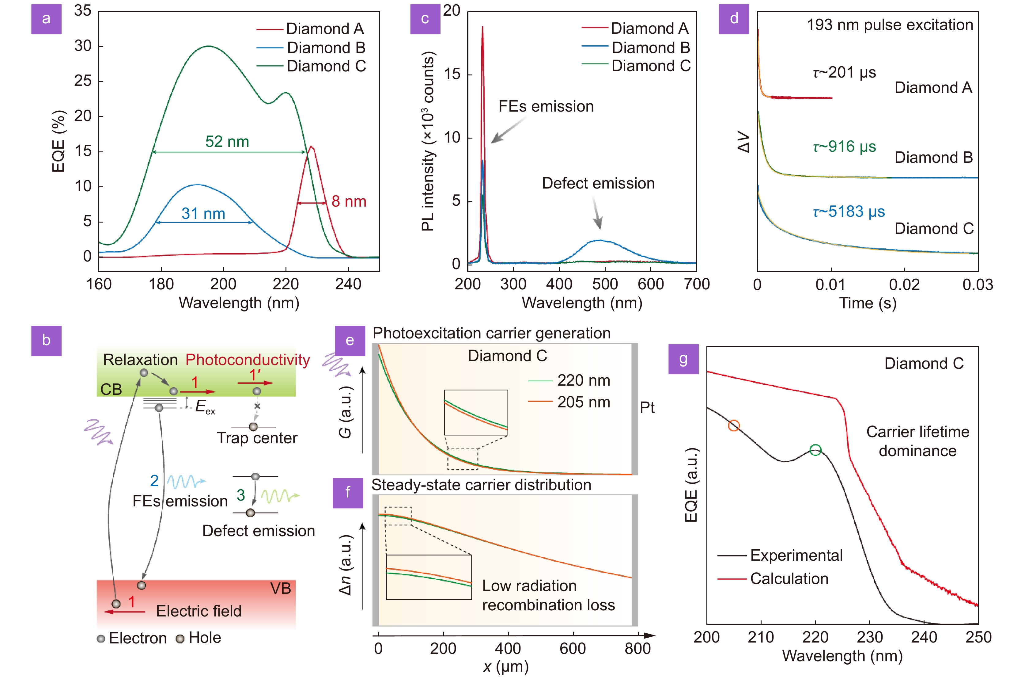
Figure 3.
Broadband photodetection mechanism based on diamonds B and C. (a) EQE comparison of photodetectors based on diamonds A, B, and C. (b) Schematic diagram of main possible physical processes of diamonds B and C under photoexcitation. (c) PL spectra of diamonds A, B, and C under 193 nm pulse excitation. (d) Voltage signals (ΔV) of photodetectors based on diamonds A, B, and C under 193 nm pulse excitation. Lifetime of 201 μs, 916 μs, and 5183 μs can be obtained by falling edges, respectively. (e) and (f) Spatial distribution of photoexcited excess carrier generation rate G and steady-state carriers within diamond C-based device. The two wavelengths selected are 205 nm and 220 nm, respectively. (g) Experimental EQE and simplified calculated EQE of the diamond C-based photodetector with a consistent trend shown between.
-
Figure 4.
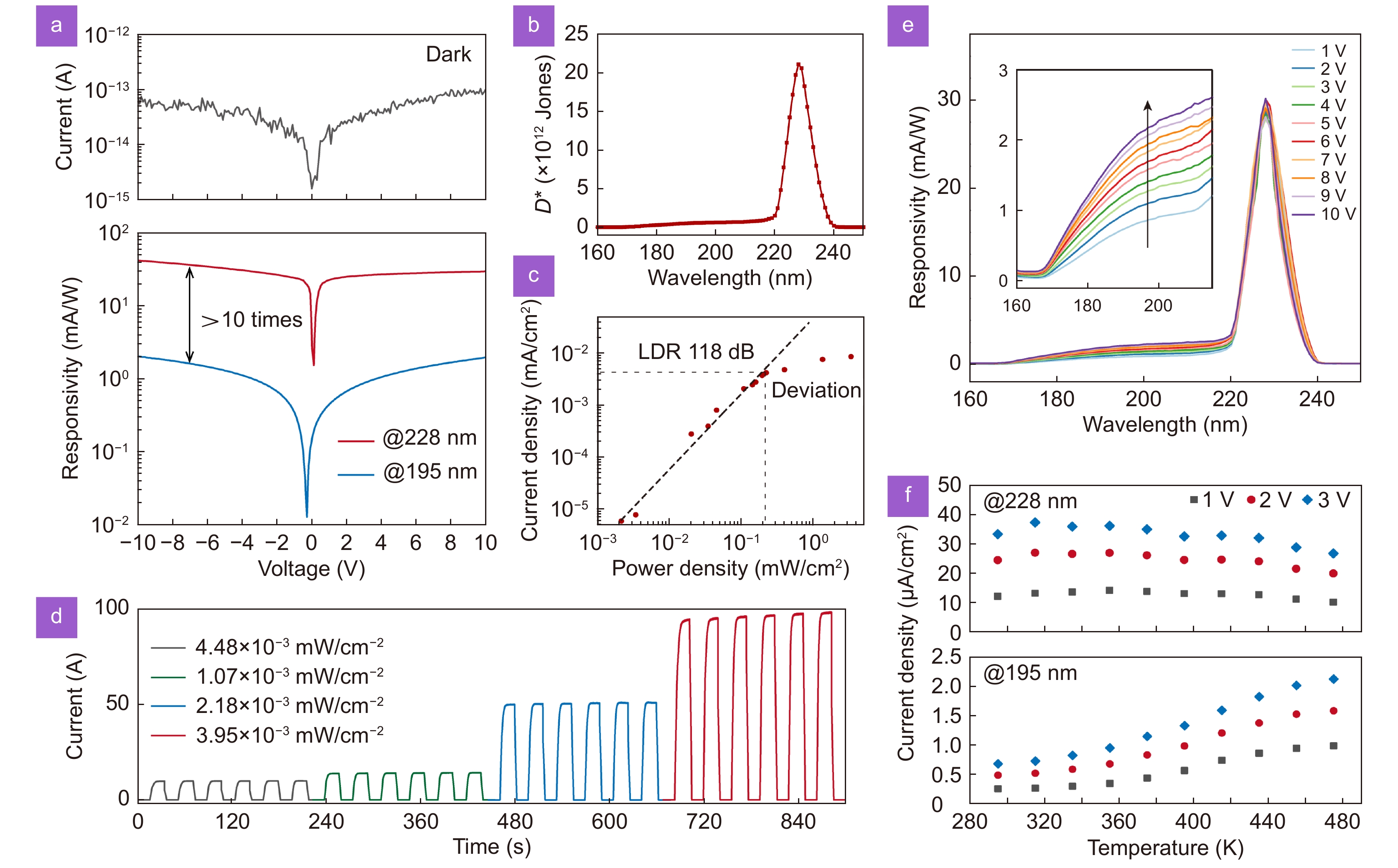
Performance of narrowband photodetectors based on diamond A. (a) Dark current and responsivity at different bias under 228 nm and 185 nm irradiation. (b) Specific detectivity (D*) spectrum under 1 V bias. (c) Linear dynamic range (LDR) of the device under 1 V bias and 228 nm irradiation. (d) Temporal response under 1 V bias and 228 nm irradiation with different optical powers. (e) Responsivity spectra under 0-10 V bias. The inset is an enlarged view of the shortwave region. (f) Measurements on varying temperatures of the device under 0–3 V bias. Different trends are exhibited under 228 nm and 185 nm irradiation.
-
Figure 5.
Imaging demonstration of narrowband photodetectors for DUV light sources. (a) Photograph of 222 nm excimer lamp. (b) Imaging of the device for excimer lamp with a size of 65 × 22 pixels whose size is 500 μm × 500 μm. (c) Normalized excimer lamp spectrum and EQE of the device, where an overlap can be observed. (d) Photograph of mercury lamp. (e) Imaging of the device for mercury lamp. (f) Normalized mercury lamp spectrum and EQE of the device, where only a weak overlap is found.


