
 E-mail Alert
 RSS
RSS
| Citation: |
Min JH, Lee K, Chung TH, Min JW, Li KH et al. Large-scale and high-quality III-nitride membranes through microcavity-assisted crack propagation by engineering tensile-stressed Ni layers. Opto-Electron Sci 1, 220016 (2022). doi: 10.29026/oes.2022.220016

|
Large-scale and high-quality III-nitride membranes through microcavity-assisted crack propagation by engineering tensile-stressed Ni layers
-
Abstract
Epitaxially grown III-nitride alloys are tightly bonded materials with mixed covalent-ionic bonds. This tight bonding presents tremendous challenges in developing III-nitride membranes, even though semiconductor membranes can provide numerous advantages by removing thick, inflexible, and costly substrates. Herein, cavities with various sizes were introduced by overgrowing target layers, such as undoped GaN and green LEDs, on nanoporous templates prepared by electrochemical etching of n-type GaN. The large primary interfacial toughness was effectively reduced according to the design of the cavity density, and the overgrown target layers were then conveniently exfoliated by engineering tensile-stressed Ni layers. The resulting III-nitride membranes maintained high crystal quality even after exfoliation due to the use of GaN-based nanoporous templates with the same lattice constant. The microcavity-assisted crack propagation process developed for the current III-nitride membranes forms a universal process for developing various kinds of large-scale and high-quality semiconductor membranes.-
Keywords:
- III-nitride alloys /
- membranes /
- nanoporous /
- Ni stressor /
- light-emitting diodes /
- ultraviolet photodetectors
-

-
References
[1] Nakamura S, Mukai T, Senoh M. Candela‐class high‐brightness InGaN/AlGaN double‐heterostructure blue‐light‐emitting diodes. Appl Phys Lett 64, 1687–1689 (1994). doi: 10.1063/1.111832 [2] Kneissl M, Seong TY, Han J, Amano H. The emergence and prospects of deep-ultraviolet light-emitting diode technologies. Nat Photonics 13, 233–244 (2019). doi: 10.1038/s41566-019-0359-9 [3] Chowdhury S, Mishra UK. Lateral and vertical transistors using the AlGaN/GaN heterostructure. IEEE Trans Electron Devices 60, 3060–3066 (2013). doi: 10.1109/TED.2013.2277893 [4] Kang CH, Liu GY, Lee C, Alkhazragi O, Wagstaff JM et al. Semipolar (2021) InGaN/GaN micro-photodetector for gigabit-per-second visible light communication. Appl Phys Express 13, 014001 (2020). doi: 10.7567/1882-0786/ab58eb [5] Dreyer CE, Janotti A, Van De Walle CG. Brittle fracture toughnesses of GaN and AlN from first-principles surface-energy calculations. Appl Phys Lett 106, 212103 (2015). doi: 10.1063/1.4921855 [6] Park J, Song KM, Jeon SR, Baek JH, Ryu SW. Doping selective lateral electrochemical etching of GaN for chemical lift-off. Appl Phys Lett 94, 221907 (2009). doi: 10.1063/1.3153116 [7] Ueda T, Ishida M, Yuri M. Separation of thin GaN from sapphire by laser lift-off technique. Jpn J Appl Phys 50, 041001 (2011). doi: 10.1143/JJAP.50.041001 [8] Park SH, Yuan G, Chen DT, Xiong KL, Song J et al. Wide bandgap III-nitride nanomembranes for optoelectronic applications. Nano Lett 14, 4293–4298 (2014). doi: 10.1021/nl5009629 [9] Jang LW, Jeon DW, Chung TH, Polyakov AY, Cho HS et al. Facile fabrication of free-standing light emitting diode by combination of wet chemical etchings. ACS Appl Mater Interfaces 6, 985–989 (2014). doi: 10.1021/am404285s [10] Zhang Y, Leung B, Han J. A liftoff process of GaN layers and devices through nanoporous transformation. Appl Phys Lett 100, 181908 (2012). doi: 10.1063/1.4711218 [11] Kobayashi Y, Kumakura K, Akasaka T, Makimoto T. Layered boron nitride as a release layer for mechanical transfer of GaN-based devices. Nature 484, 223–227 (2012). doi: 10.1038/nature10970 [12] Kim Y, Cruz SS, Lee K, Alawode BO, Choi C et al. Remote epitaxy through graphene enables two-dimensional material-based layer transfer. Nature 544, 340–343 (2017). doi: 10.1038/nature22053 [13] Park JH, Lee JY, Park MD, Min JH, Lee JS et al. Influence of temperature‐dependent substrate decomposition on graphene for separable GaN growth. Adv Mater Interfaces 6, 1900821 (2019). doi: 10.1002/admi.201900821 [14] Lee JY, Min JH, Bae SY, Park MD, Jeong WL et al. Multiple epitaxial lateral overgrowth of GaN thin films using a patterned graphene mask by metal organic chemical vapor deposition. J Appl Cryst 53, 1502–1508 (2020). doi: 10.1107/S1600576720012856 [15] Kong W, Li HS, Qiao K, Kim Y, Lee K et al. Polarity governs atomic interaction through two-dimensional materials. Nat Mater 17, 999–1004 (2018). doi: 10.1038/s41563-018-0176-4 [16] Jia YQ, Ning J, Zhang JC, Yan CC, Wang BY et al. Transferable GaN enabled by selective nucleation of AlN on graphene for high‐brightness violet light‐emitting diodes. Adv Opt Mater 8, 1901632 (2019). [17] Ke WC, Liang ZY, Tesfay ST, Chiang CY, Yang CY et al. Epitaxial growth and characterization of GaN thin films on graphene/sapphire substrate by embedding a hybrid-AlN buffer layer. Appl Surf Sci 494, 644–650 (2019). doi: 10.1016/j.apsusc.2019.07.211 [18] Wang N, Wang P, Wang FZ, He HP, Huang JY et al. Improved epitaxy of ZnO films by regulating the layers of graphene. Appl Surf Sci 585, 152709 (2022). doi: 10.1016/j.apsusc.2022.152709 [19] Bedell SW, Shahrjerdi D, Hekmatshoar B, Fogel K, Lauro PA et al. Kerf-less removal of Si, Ge, and III–V layers by controlled spalling to enable low-cost PV technologies. IEEE J Photovolt 2, 141–147 (2012). doi: 10.1109/JPHOTOV.2012.2184267 [20] Lee YH, Kim YJ, Han SMJ, Song HE, Oh J. Sub-5 μm-thick spalled single crystal Si foils by decoupling crack initiation and propagation. Appl Phys Lett 109, 132101 (2016). doi: 10.1063/1.4963292 [21] Kim J, Park H, Hannon JB, Bedell SW, Fogel K et al. Layer-resolved graphene transfer via engineered strain layers. Science 342, 833–836 (2013). doi: 10.1126/science.1242988 [22] Shim J, Bae SH, Kong W, Lee D, Qiao K et al. Controlled crack propagation for atomic precision handling of wafer-scale two-dimensional materials. Science 362, 665–670 (2018). doi: 10.1126/science.aat8126 [23] Min JH, Li KH, Kim YH, Min JW, Kang CH et al. Toward large-scale Ga2O3 membranes via quasi-van der waals epitaxy on epitaxial graphene layers. ACS Appl Mater Interfaces 13, 13410–13418 (2021). doi: 10.1021/acsami.1c01042 [24] Zhang C, Park SH, Chen DT, Lin DW, Xiong W et al. Mesoporous GaN for photonic engineering—highly reflective GaN mirrors as an example. ACS Photonics 2, 980–986 (2015). doi: 10.1021/acsphotonics.5b00216 [25] Lee KJ, Min JW, Turedi B, Alsalloum AY, Min JH et al. Nanoporous GaN/n-type GaN: a cathode structure for ITO-free perovskite solar cells. ACS Energy Lett 5, 3295–3303 (2020). doi: 10.1021/acsenergylett.0c01621 [26] Griffin PH, Oliver RA. Porous nitride semiconductors reviewed. J Phys D Appl Phys 53, 383002 (2020). doi: 10.1088/1361-6463/ab9570 [27] Koleske DD, Wickenden AE, Henry RL, Culbertson JC, Twigg ME. GaN decomposition in H2 and N2 at MOVPE temperatures and pressures. J Cryst Growth 223, 466–483 (2001). doi: 10.1016/S0022-0248(01)00617-0 [28] Ghannam MY, Alomar AS, Poortmans J, Mertens RP. Interpretation of macropore shape transformation in crystalline silicon upon high temperature processing. J Appl Phys 108, 074902 (2010). doi: 10.1063/1.3462448 [29] Yerino CD, Zhang Y, Leung B, Lee ML, Hsu TC et al. Shape transformation of nanoporous GaN by annealing: From buried cavities to nanomembranes. Appl Phys Lett 98, 251910 (2011). doi: 10.1063/1.3601861 [30] Polyakov AY, Shin M, Freitas JA, Skowronski M, Greve DW et al. On the origin of electrically active defects in AlGaN alloys grown by organometallic vapor phase epitaxy. J Appl Phys 80, 6349–6354 (1996). doi: 10.1063/1.363653 [31] Reshchikov MA, Shahedipour F, Korotkov RY, Wessels BW, Ulmer MP. Photoluminescence band near 2.9 eV in undoped GaN epitaxial layers. J Appl Phys 87, 3351–3354 (2000). doi: 10.1063/1.372348 [32] Reshchikov MA, Huang D, Yun F, Visconti P, He L et al. Unusual luminescence lines in GaN. J Appl Phys 94, 5623–5632 (2003). doi: 10.1063/1.1609632 [33] Ren FZ, Liu P, Jia SG, Tian BH, Su JH. Adhesion strength of Ni film on Ti substrate characterized by three-point bend test, peel test and theoretic calculation. Mater Sci Eng A 419, 233–237 (2006). doi: 10.1016/j.msea.2005.12.024 -
Supplementary Information
-
Access History

Figures(4)
Article Metrics

Export File
Citation
Min JH, Lee K, Chung TH, Min JW, Li KH et al. Large-scale and high-quality III-nitride membranes through microcavity-assisted crack propagation by engineering tensile-stressed Ni layers. Opto-Electron Sci 1, 220016 (2022). doi: 10.29026/oes.2022.220016
Format
Content
 DownLoad:
-
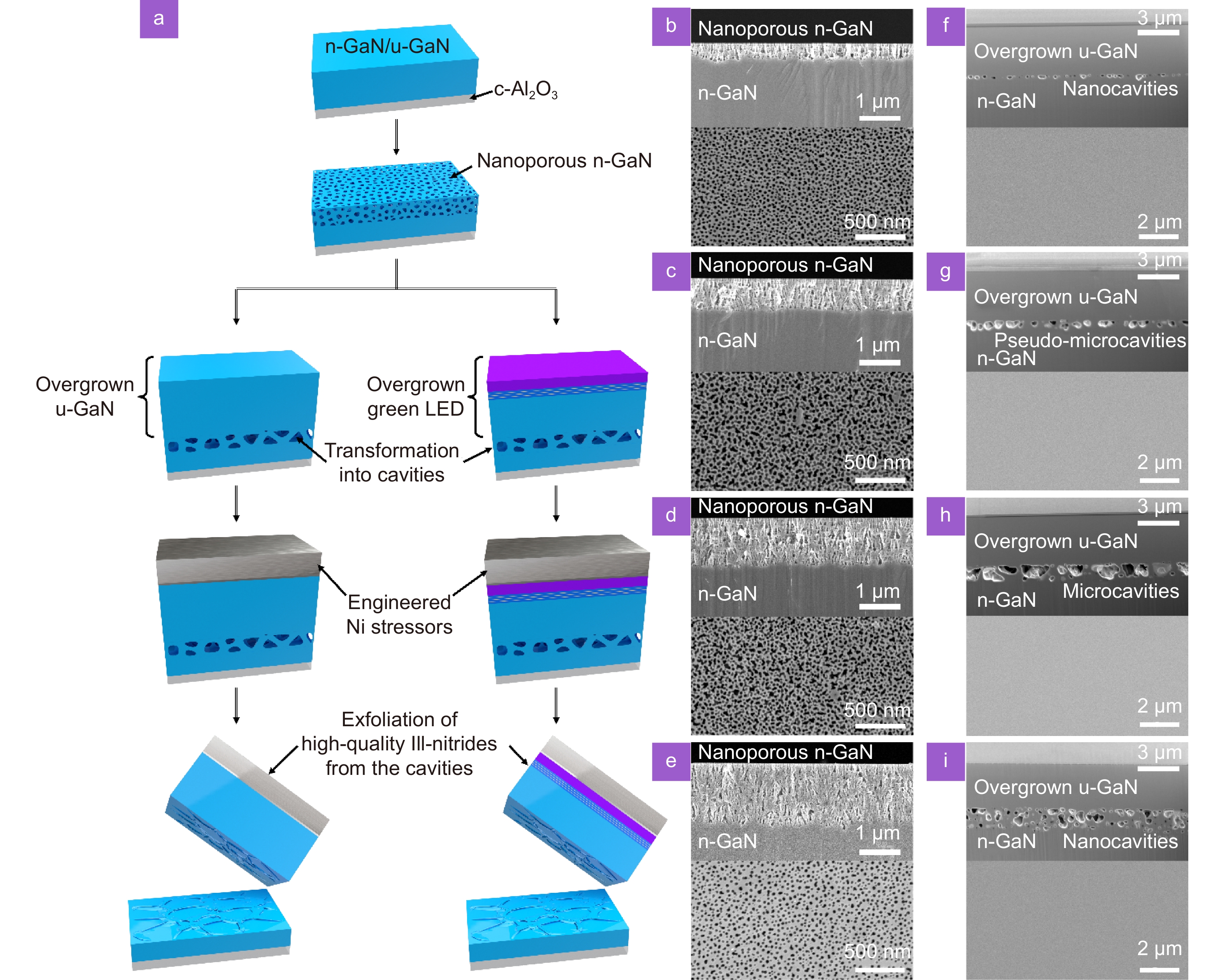
Figure 1.
(a) A summary of the schematic illustration for the exfoliation of large-scale and high-quality III-nitride layers through microcavity-assisted crack propagation to achieve membrane-based applications such as surface-emitting vertical-type green LEDs (V-LEDs), as well as surface-absorbing vertical-type ultraviolet photodetectors (V-UV PDs). (b–e) Scanning electron microscope (SEM) images of cross-sectional and top views for the nanoporous n-GaN layers manufactured by various EC etching conditions: 15 V for 5 min (b), 10 min (c), and 15 min (d) by using heavily doped n-GaN, and 20 V for 15 min (e) by using lightly doped n-GaN. In order, each nanoporous n-GaN is designated as ‘Nanoporous 1’, ‘Nanoporous 2’, ‘Nanoporous 3’, and ‘Nanoporous 4’. The porosity and depth of the nanoporous structures can be varied through the input voltage, time, and doping concentration. (f–i) Focused ion beam (FIB)-SEM and SEM images of cross-sectional and top views for the overgrown u-GaN layers. The overgrown u-GaN layers on the nanoporous structures are named ‘Overgrown u-GaN 1’, ‘Overgrown u-GaN 2’, ‘Overgrown u-GaN 3’, and ‘Overgrown u-GaN 4’. After overgrowing the u-GaN layers, cavities were formed with different shapes and sizes according to the original nanoporous structures.
-
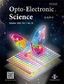
Figure 2.
(a) A representative schematic illustration of microcavity-assisted crack propagation. (b) The values of the interfacial toughness of GaN depending on the density of the cavities (blue-colored line) and the applied interfacial toughness through the Ni stressors (black-colored line). The maximum value of the interfacial toughness is 6.38 J/m2 with reference to GaN (002). The blue- and black-colored spheres are the experimental data points obtained from the estimated cavity densities and Ni stressors, respectively. (c) A digital camera image of a u-GaN membrane acquired from ‘Overgrown u-GaN 3’ after successful exfoliation with the well-engineered Ni stressor. The inset shows the substrate side after exfoliation. (d–e) Representative schematic illustrations for the u-GaN membrane side and the substrate side and the related SEM and FIB-SEM images for the top, bird’s eye, and cross-sectional views, respectively. The microsized islands were observed on the surface of the membrane and the substrate after exfoliation. (f–i) Results of the various XRD measurements to check the quality of the u-GaN membrane after exfoliation: ω-2θ scan (f), ω rocking curve for (002) orientations (g), ϕ scan for (102) orientations (h), and ω rocking curve for (102) orientations (i).
-
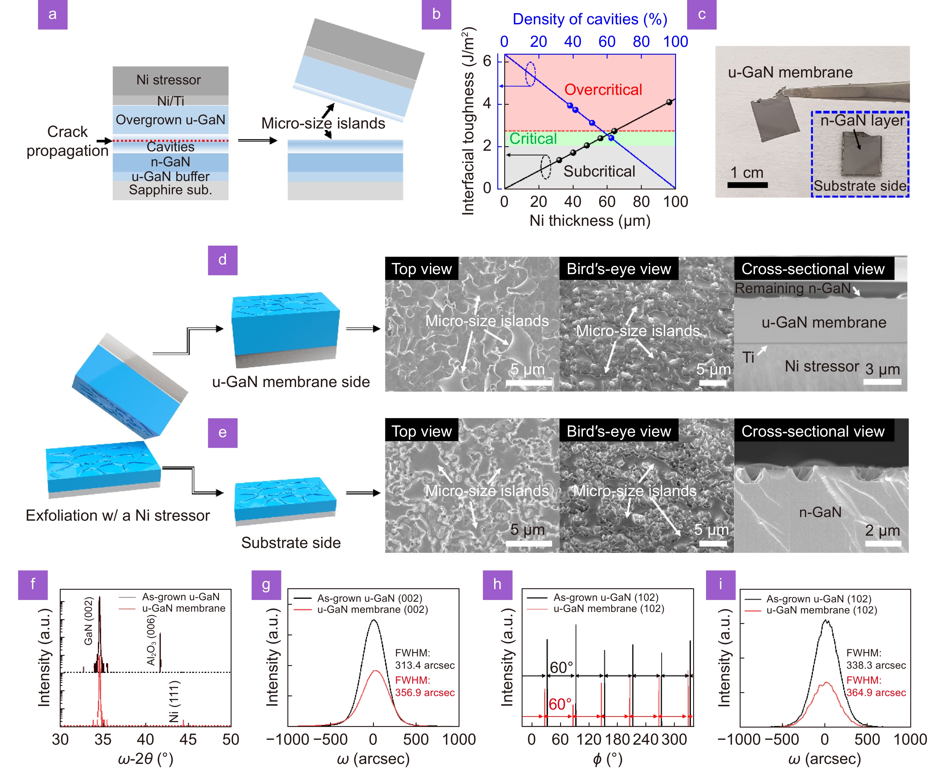
Figure 3.
(a) SEM images of the top and cross-sectional views for an overgrown green LED on ‘Nanoporous 2’. The blue-colored dash indicates the detailed top-most areas of the green LED through a high-angle annular dark-field scanning transmission electron microscope (STEM) image and the related STEM-energy dispersive X-ray analysis mapping. (b) A digital camera image of a green LED membrane exfoliated from cavities with a well-engineered Ni stressor. The inset shows the substrate side after exfoliation. (c) Results of photoluminescence of the green LED before and after exfoliation. The 473 nm Cobolt laser was used for the as-grown green LED and the green LED membrane due to the peak wavelength of the green LED (~533 nm), and the He-Cd 325 nm laser was employed for the substrate side. (d-e) Representative schematic illustrations for the green LED membrane side and the substrate side and the related SEM and FIB-SEM images for the top, bird’s eye, and cross-sectional views, respectively. Wider microsized islands were observed on the surfaces of the membrane and the substrate compared to the u-GaN membrane.
-
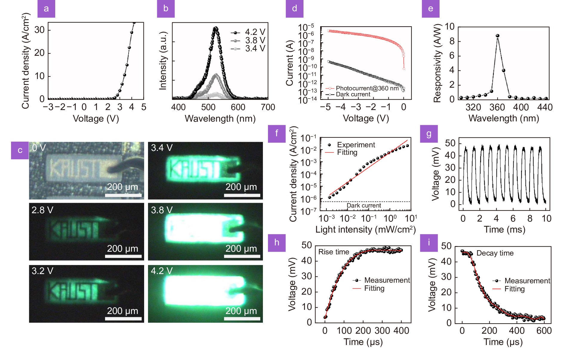
Figure 4.
Device applications using green LEDs and u-GaN membranes. (a–b) Current density-voltage and electroluminescence (EL) spectral characteristics of the V-LEDs. The peak wavelength of the V-LEDs was ~525 nm. (c) Optical microscope EL images of the green V-LEDs according to input voltages. (d) Current–voltage characteristics of the V-UV PDs under illumination at 360 nm (0.53 mW/cm2). (e) Responsivity of the V-UV PDs at –5 V according to wavelengths from 300 nm to 440 nm. The peak responsivity was 8.78 A/W at 360 nm, and the responsivity spectrum showed a high selectivity of the wavelength over 350−370 nm. (f) Measured values of the current density depending on the illuminated light intensity from 1.39 × 10⁻³ to 6.71 mW/cm2 at –5 V. (g) Time response characteristics measured by using a 375 nm laser diode at –5 V. The UV laser pulses were 1 kHz. (h-i) The zoom-in time response curve and its biexponential fitting curves to obtain the rise time and decay time. The rise and decay times are 145 and 205 μs, respectively.


