
 E-mail Alert
 RSS
RSS
| Citation: |
Jing XL, Liao QM, Liang MS et al. Three-dimensional measurement enabled by single-layer all-in-one transmitting-receipting optical metasystem. Opto-Electron Adv 8, 240299 (2025). doi: 10.29026/oea.2025.240299

|
Three-dimensional measurement enabled by single-layer all-in-one transmitting-receipting optical metasystem
-
Abstract
Optical three-dimensional (3D) measurement is a critical tool in micro-nano manufacturing, the automotive industry, and medical technology due to its nondestructive nature, high precision, and sensitivity. However, passive light field system still requires a refractive primary lens to collect light of the scene, and structured light can not work well with the highly refractive object. Meta-optics, known for being lightweight, compact, and easily integrable, has enabled advancements in passive metalens-array light fields and active structured light techniques. Here, we propose and experimentally validate a novel 3D measurement metasystem. It features a transmitting metasurface generating chromatic line focuses as depth markers and a symmetrically arranged receiving metasurface collecting depth-dependent spectral responses. A lightweight, physically interpretable algorithm processes these data to yield high-precision depth information efficiently. Experiments on metallic and wafer materials demonstrate a depth accuracy of ±20 µm and lateral accuracy of ±10 µm. This single-layer optical metasystem, characterized by simplicity, micro-level accuracy, easy installation and scalability, shows potential for diverse applications, including process control, surface morphology analysis, and production measurement.-
Keywords:
- metasystem /
- 3D reconstruction /
- dispersion engineering
-

-
References
[1] Zhang QY, Wen W, Hu SX et al. Nothosaur foraging tracks from the Middle Triassic of southwestern China. Nat Commun 5, 3973 (2014). doi: 10.1038/ncomms4973 [2] Liu WW, Ma DN, Li ZC et al. Aberration-corrected three-dimensional positioning with a single-shot metalens array. Optica 7, 1706–1713 (2020). doi: 10.1364/OPTICA.406039 [3] Shaked NT, Boppart SA, Wang LV et al. Label-free biomedical optical imaging. Nat Photonics 17, 1031–1041 (2023). doi: 10.1038/s41566-023-01299-6 [4] Kim K. Single-shot light-field microscopy: an emerging tool for 3D biomedical imaging. BioChip J 16, 397–408 (2022). doi: 10.1007/s13206-022-00077-w [5] Zang HF, Xi Z, Zhang ZY et al. Ultrasensitive and long-range transverse displacement metrology with polarization-encoded metasurface. Sci Adv 8, eadd1973 (2022). doi: 10.1126/sciadv.add1973 [6] Zang HF, Zhang ZY, Huang ZT et al. High-precision two-dimensional displacement metrology based on matrix metasurface. Sci Adv 10, eadk2265 (2024). doi: 10.1126/sciadv.adk2265 [7] Ferreras Paz V, Peterhänsel S, Frenner K et al. Solving the inverse grating problem by white light interference Fourier scatterometry. Light Sci Appl 1, e36 (2012). doi: 10.1038/lsa.2012.36 [8] Shimizu Y, Chen LC, Kim DW et al. An insight into optical metrology in manufacturing. Meas Sci Technol 32, 042003 (2021). [9] Wu ZJ, Wang HR, Chen FF et al. Dynamic 3D shape reconstruction under complex reflection and transmission conditions using multi-scale parallel single-pixel imaging. Light Adv Manuf 5, 373–384 (2024). [10] Choi E, Kim G, Yun J et al. 360° structured light with learned metasurfaces. Nat Photonics 18, 848–855 (2024). doi: 10.1038/s41566-024-01450-x [11] Kim G, Kim Y, Yun J et al. Metasurface-driven full-space structured light for three-dimensional imaging. Nat Commun 13, 5920 (2022). doi: 10.1038/s41467-022-32117-2 [12] Georgiev T, Lumsdaine A. Reducing plenoptic camera artifacts. Comput Graphics Forum 29, 1955–1968 (2010). doi: 10.1111/j.1467-8659.2010.01662.x [13] Zeller N, Quint F, Stilla U. Depth estimation and camera calibration of a focused plenoptic camera for visual odometry. ISPRS J Photogramm Remote Sens 118, 83–100 (2016). doi: 10.1016/j.isprsjprs.2016.04.010 [14] Kim I, Martins RJ, Jang J et al. Nanophotonics for light detection and ranging technology. Nat Nanotechnol 16, 508–524 (2021). doi: 10.1038/s41565-021-00895-3 [15] Hu XM, Xu WZ, Fan QB et al. Metasurface-based computational imaging: a review. Adv Photonics 6, 014002 (2024). [16] Zhu WM, Song QH, Yan LB et al. A flat lens with tunable phase gradient by using random access reconfigurable metamaterial. Adv Mater 27, 4739–4743 (2015). doi: 10.1002/adma.201501943 [17] Tseng ML, Hsiao HH, Chu CH et al. Metalenses: advances and applications. Adv Opt Mater 6, 1800554 (2018). doi: 10.1002/adom.201800554 [18] Xiong B, Liu Y, Xu YH et al. Breaking the limitation of polarization multiplexing in optical metasurfaces with engineered noise. Science 379, 294–299 (2023). doi: 10.1126/science.ade5140 [19] So S, Mun J, Park J et al. Revisiting the design strategies for metasurfaces: fundamental physics, optimization, and beyond. Adv Mater 35, 2206399 (2023). doi: 10.1002/adma.202206399 [20] Yu NF, Capasso F. Flat optics with designer metasurfaces. Nat Mater 13, 139–150 (2014). doi: 10.1038/nmat3839 [21] Xie YY, Ni PN, Wang QH et al. Metasurface-integrated vertical cavity surface-emitting lasers for programmable directional lasing emissions. Nat Nanotechnol 15, 125–130 (2020). doi: 10.1038/s41565-019-0611-y [22] Wang QH, Ni PN, Xie YY et al. On‐chip generation of structured light based on metasurface optoelectronic integration. Laser Photonics Rev 15, 2000385 (2021). doi: 10.1002/lpor.202000385 [23] Jing XL, Li Y, Li JJ et al. Active 3D positioning and imaging modulated by single fringe projection with compact metasurface device. Nanophotonics 12, 1923–1930 (2023). doi: 10.1515/nanoph-2023-0112 [24] Liu XY, Zhang JC, Leng BR et al. Edge enhanced depth perception with binocular meta-lens. Opto-Electron Sci 3, 230033 (2024). doi: 10.29026/oes.2024.230033 [25] Yang Y, Seong J, Choi M et al. Integrated metasurfaces for re-envisioning a near-future disruptive optical platform. Light Sci Appl 12, 152 (2023). doi: 10.1038/s41377-023-01169-4 [26] Xiong YF, Xu F. Multifunctional integration on optical fiber tips: challenges and opportunities. Adv Photonics 2, 064001 (2020). [27] Liu MZ, Zhu WQ, Huo PC et al. Multifunctional metasurfaces enabled by simultaneous and independent control of phase and amplitude for orthogonal polarization states. Light Sci Appl 10, 107 (2021). doi: 10.1038/s41377-021-00552-3 [28] Gao H, Fan XH, Wang YX et al. Multi-foci metalens for spectra and polarization ellipticity recognition and reconstruction. Opto-Electron Sci 2, 220026 (2023). doi: 10.29026/oes.2023.220026 [29] Jung C, Lee E, Rho J. The rise of electrically tunable metasurfaces. Sci Adv 10, eado8964 (2024). doi: 10.1126/sciadv.ado8964 [30] Wen DD, Yue FY, Ardron M et al. Multifunctional metasurface lens for imaging and Fourier transform. Sci Rep 6, 27628 (2016). doi: 10.1038/srep27628 [31] Jiang SB, Deng WJ, Wang ZS et al. Ka-Band metalens antenna empowered by physics-assisted particle swarm optimization (PA-PSO) algorithm. Opto-Electron Sci 3, 240014 (2024). doi: 10.29026/oes.2024.240014 [32] Engay E, Huo DW, Malureanu R et al. Polarization-dependent all-dielectric metasurface for single-shot quantitative phase imaging. Nano Lett 21, 3820–3826 (2021). doi: 10.1021/acs.nanolett.1c00190 [33] Zhou JX, Tian FL, Hu J et al. Eagle‐eye inspired meta‐device for phase imaging. Adv Mater 36, 2402751 (2024). doi: 10.1002/adma.202402751 [34] Guo Q, Shi ZJ, Huang YW et al. Compact single-shot metalens depth sensors inspired by eyes of jumping spiders. Proc Natl Acad Sci USA 116, 22959–22965 (2019). doi: 10.1073/pnas.1912154116 [35] Lin RJ, Su VC, Wang SM et al. Achromatic metalens array for full-colour light-field imaging. Nat Nanotechnol 14, 227–231 (2019). doi: 10.1038/s41565-018-0347-0 [36] Fan QB, Xu WZ, Hu XM et al. Trilobite-inspired neural nanophotonic light-field camera with extreme depth-of-field. Nat Commun 13, 2130 (2022). doi: 10.1038/s41467-022-29568-y [37] Liang HW, Martins A, Borges BHV et al. High performance metalenses: numerical aperture, aberrations, chromaticity, and trade-offs. Optica 6, 1461–1470 (2019). doi: 10.1364/OPTICA.6.001461 [38] Engelberg J, Levy U. Achromatic flat lens performance limits. Optica 8, 834–845 (2021). doi: 10.1364/OPTICA.422843 [39] Shrestha S, Overvig AC, Lu M et al. Broadband achromatic dielectric metalenses. Light Sci Appl 7, 85 (2018). doi: 10.1038/s41377-018-0078-x [40] Li ZL, Dai Q, Mehmood MQ et al. Full-space cloud of random points with a scrambling metasurface. Light Sci Appl 7, 63 (2018). doi: 10.1038/s41377-018-0064-3 [41] Jing XL, Zhao RZ, Li X et al. Single-shot 3D imaging with point cloud projection based on metadevice. Nat Commun 13, 7842 (2022). doi: 10.1038/s41467-022-35483-z [42] Chen R, Shao YF, Zhou Y et al. A semisolid micromechanical beam steering system based on micrometa-lens arrays. Nano Lett 22, 1595–1603 (2022). doi: 10.1021/acs.nanolett.1c04493 [43] Park J, Jeong BG, Kim SI et al. All-solid-state spatial light modulator with independent phase and amplitude control for three-dimensional LiDAR applications. Nat Nanotechnol 16, 69–76 (2021). doi: 10.1038/s41565-020-00787-y [44] Blinn JF. Models of light reflection for computer synthesized pictures. ACM SIGGRAPH Comput Graphics 11, 192–198 (1977). doi: 10.1145/965141.563893 -
Supplementary Information
Supplementary information for Three-dimensional measurement enabled bysingle-layer all-in-one transmitting-receiptingoptical metasystem 
-
Access History
Figures(4)
Tables(1)
Article Metrics


Export File
Citation
Jing XL, Liao QM, Liang MS et al. Three-dimensional measurement enabled by single-layer all-in-one transmitting-receipting optical metasystem. Opto-Electron Adv 8, 240299 (2025). doi: 10.29026/oea.2025.240299
Format
Content
 DownLoad:
-
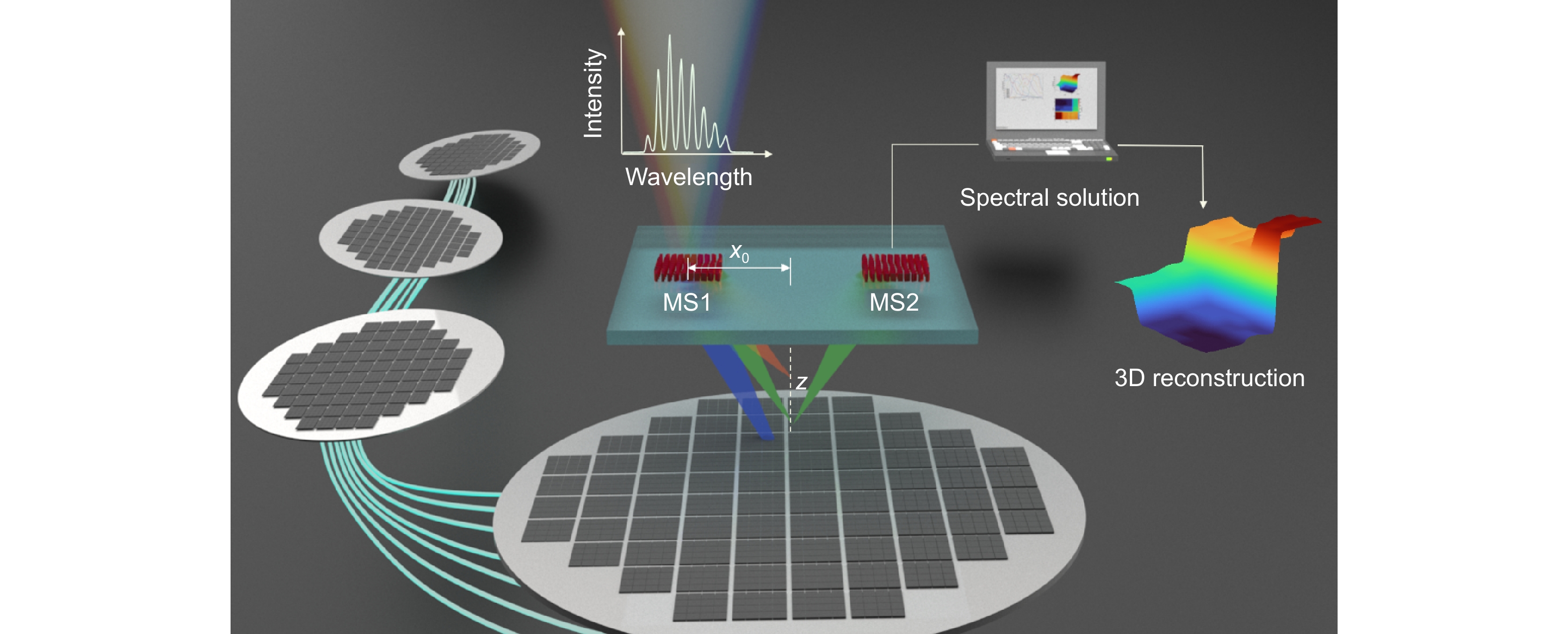
Figure 1.
Schematic diagram of the three-dimensional measurement metasystem. The integrated transceiver design enables detection of processed structures on the wafer surface, facilitating a compact, miniaturized, non-contact inspection system.
-
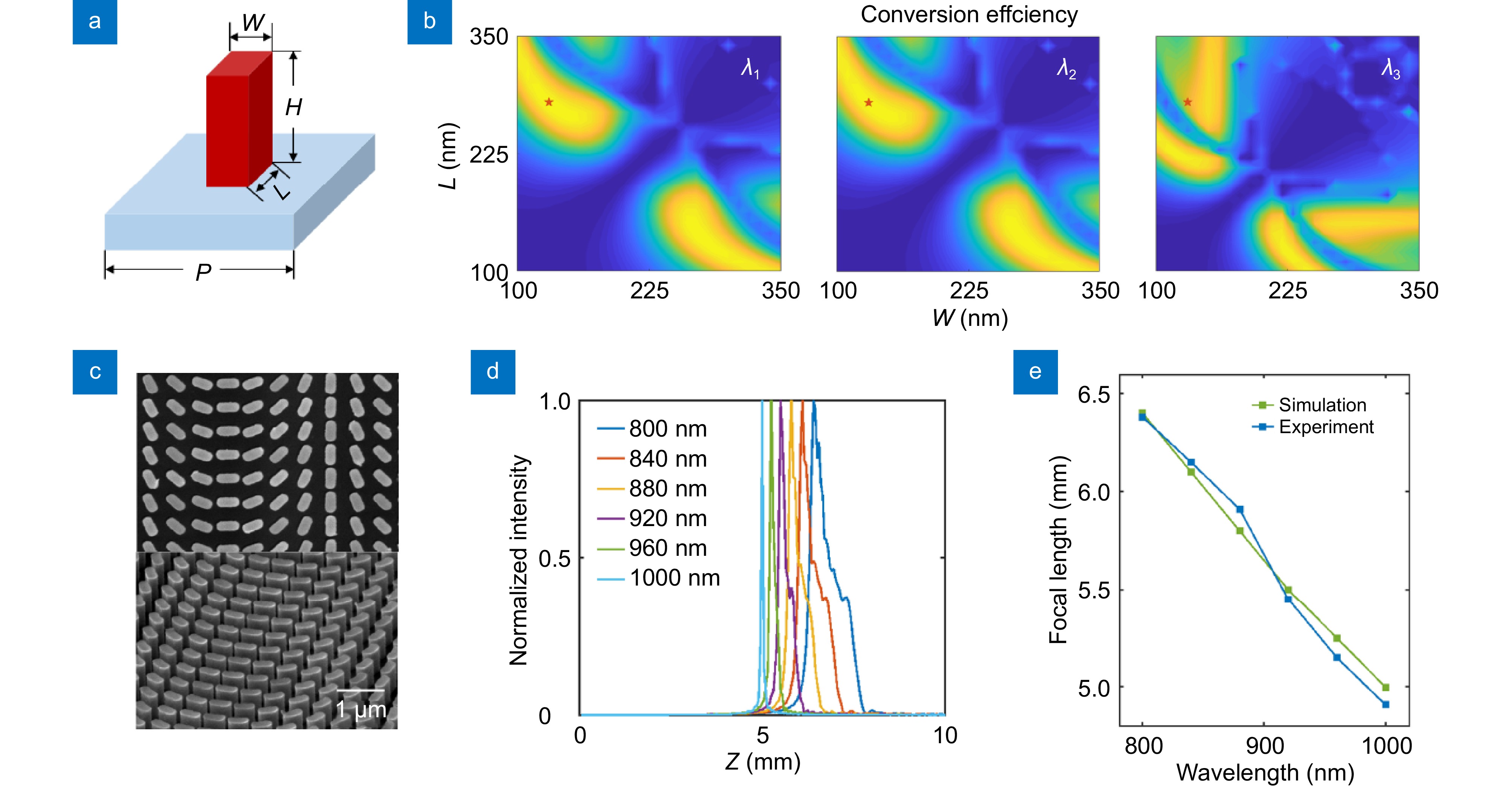
Figure 2.
(a) Schematic diagram of the metasurface unit structure. (b) Polarization conversion efficiency (range 0-1) of the selected unit structure at the starting wavelength, middle wavelength, and cutoff wavelength. (c) SEM image of the fabricated metasurface sample. (d) Focusing behavior along the Z direction at a distance of 3.5 mm from the optical axis for different wavelengths. (e) Comparison of experimental results and simulation results for focusing effects at different wavelengths.
-
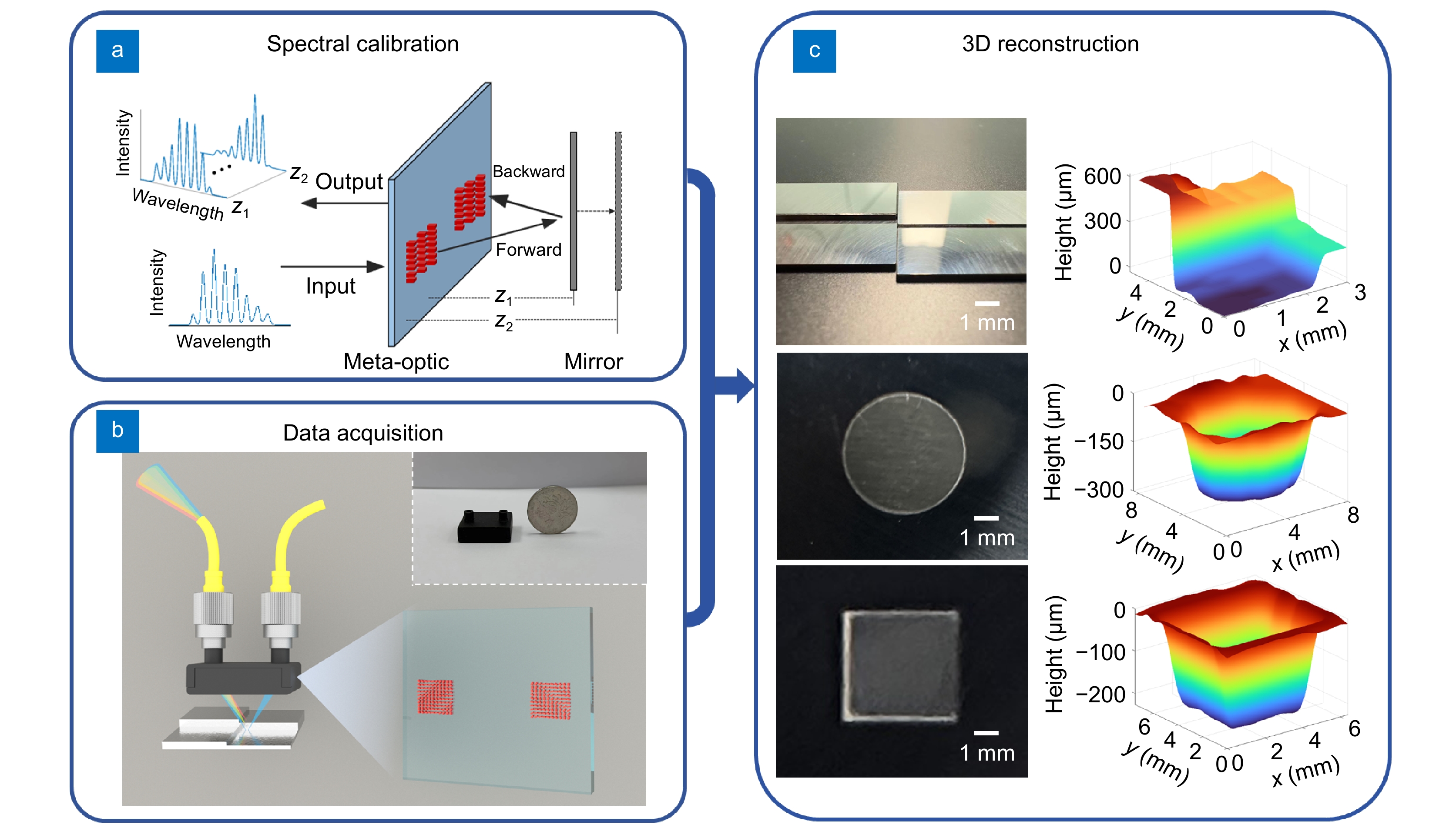
Figure 3.
(a) Schematic diagram of data calibration. (b) Schematic diagram of data acquisition for the object under test. (c) 3D reconstruction result.
-
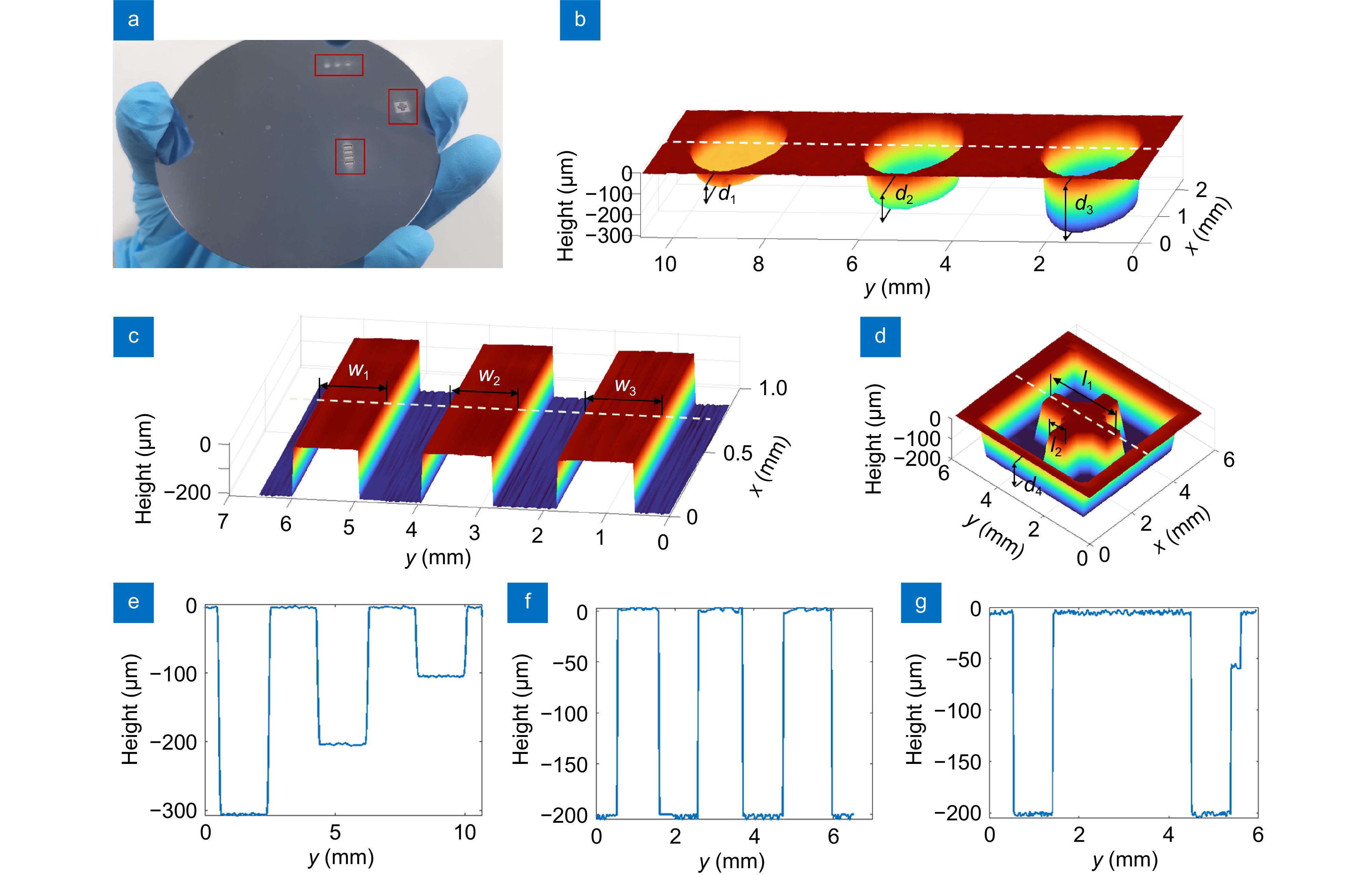
Figure 4.
(a) Diagram of the wafer under test, with the red frame indicating the patterns to be measured. (b) Reconstruction results of circular holes at different depths. (c) Reconstruction results of gratings with different widths. (d) Reconstruction results of cross-shaped markers. (e) Restoration results of circular holes along the y direction at different depths. (f) Restoration results of gratings along the y direction with different widths. (g) Restoration results of cross-shaped markers along the y direction.


