
 E-mail Alert
 RSS
RSS
| Citation: |
Lin ZY, Liu K, Cao T, Hong MH. Microsphere femtosecond laser sub-50 nm structuring in far field via non-linear absorption. Opto-Electron Adv 6, 230029 (2023). doi: 10.29026/oea.2023.230029

|
Microsphere femtosecond laser sub-50 nm structuring in far field via non-linear absorption
-
Abstract
Creation of arbitrary features with high resolution is critically important in the fabrication of nano-optoelectronic devices. Here, sub-50 nm surface structuring is achieved directly on Sb2S3 thin films via microsphere femtosecond laser irradiation in far field. By varying laser fluence and scanning speed, nano-feature sizes can be flexibly tuned. Such small patterns are attributed to the co-effect of microsphere focusing, two-photons absorption, top threshold effect, and high-repetition-rate femtosecond laser-induced incubation effect. The minimum feature size can be reduced down to ~30 nm (λ/26) by manipulating film thickness. The fitting analysis between the ablation width and depth predicts that the feature size can be down to ~15 nm at the film thickness of ~10 nm. A nano-grating is fabricated, which demonstrates desirable beam diffraction performance. This nano-scale resolution would be highly attractive for next-generation laser nano-lithography in far field and in ambient air.-
Keywords:
- non-linear effect /
- microsphere /
- femtosecond laser /
- far field
-

-
References
[1] Cummins C, Lundy R, Walsh JJ, Ponsinet V, Fleury G et al. Enabling future nanomanufacturing through block copolymer self-assembly: a review. Nano Today 35, 100936 (2020). doi: 10.1016/j.nantod.2020.100936 [2] Xiong YF, Xu F. Multifunctional integration on optical fiber tips: challenges and opportunities. Adv Photonics 2, 064001 (2020). doi: 10.1117/1.AP.2.6.064001 [3] Grebenko AK, Motovilov KA, Bubis AV, Nasibulin AG. Gentle patterning approaches toward compatibility with bio-organic materials and their environmental aspects. Small 18, 2200476 (2022). doi: 10.1002/smll.202200476 [4] Wang L, Kirk E, Wäckerlin C, Schneider CW, Hojeij M et al. Nearly amorphous Mo-N gratings for ultimate resolution in extreme ultraviolet interference lithography. Nanotechnology 25, 235305 (2014). doi: 10.1088/0957-4484/25/23/235305 [5] Ray D, Wang HC, Kim J, Santschi C, Martin OJF. A low-temperature annealing method for alloy nanostructures and metasurfaces: unlocking a novel degree of freedom. Adv Mater 34, 2108225 (2022). doi: 10.1002/adma.202108225 [6] Karakachian H, Rosenzweig P, Nguyen TTN, Matta B, Zakharov AA et al. Periodic nanoarray of graphene pn-junctions on silicon carbide obtained by hydrogen intercalation. Adv Funct Mater 32, 2109839 (2022). doi: 10.1002/adfm.202109839 [7] Wolf A, Dostovalov A, Bronnikov K, Skvortsov M, Wabnitz S et al. Advances in femtosecond laser direct writing of fiber Bragg gratings in multicore fibers: technology, sensor and laser applications. Opto-Electron Adv 5, 210055 (2022). doi: 10.29026/oea.2022.210055 [8] Ma ZC, Zhang YL, Han B, Chen QD, Sun HB. Femtosecond-laser direct writing of metallic micro/nanostructures: from fabrication strategies to future applications. Small Methods 2, 1700413 (2018). doi: 10.1002/smtd.201700413 [9] Qin L, Huang YQ, Xia F, Wang L, Ning JQ et al. 5 nm nanogap electrodes and arrays by super-resolution laser lithography. Nano Lett 20, 4916–4923 (2020). doi: 10.1021/acs.nanolett.0c00978 [10] Lin ZY, Ji LF, Hong MH. Approximately 30 nm nanogroove formation on single crystalline silicon surface under pulsed nanosecond laser irradiation. Nano Lett 22, 7005–7010 (2022). doi: 10.1021/acs.nanolett.2c01794 [11] Zhang JQ, Gao Y, Li C, Ju K, Tan JP et al. Laser direct writing of flexible antenna sensor for strain and humidity sensing. Opto-Electron Eng 49, 210316 (2022). doi: 10.12086/oee.2022.210316 [12] Ma ZC, Zhang YL, Han B, Hu XY, Li CH et al. Femtosecond laser programmed artificial musculoskeletal systems. Nat Commun 11, 4536 (2020). doi: 10.1038/s41467-020-18117-0 [13] Livakas N, Skoulas E, Stratakis E. Omnidirectional iridescence via cylindrically-polarized femtosecond laser processing. Opto-Electron Adv 3, 190035 (2020). doi: 10.29026/oea.2020.190035 [14] Zhang YL, Tian Y, Wang H, Ma ZC, Han DD et al. Dual-3D femtosecond laser nanofabrication enables dynamic actuation. ACS Nano 13, 4041–4048 (2019). doi: 10.1021/acsnano.8b08200 [15] Saha SK, Wang DE, Nguyen VH, Chang YN, Oakdale JS et al. Scalable submicrometer additive manufacturing. Science 366, 105–109 (2019). doi: 10.1126/science.aax8760 [16] Sugioka K, Cheng Y. Ultrafast lasers-reliable tools for advanced materials processing. Light Sci Appl 3, e149 (2014). doi: 10.1038/lsa.2014.30 [17] Lin ZY, Hong MH. Femtosecond laser precision engineering: from micron, submicron, to nanoscale. Ultrafast Sci 2021, 9783514 (2021). doi: 10.34133/2021/9783514 [18] Wang HT, Hao CL, Lin H, Wang YT, Lan T et al. Generation of super-resolved optical needle and multifocal array using graphene oxide metalenses. Opto-Electron Adv 4, 200031 (2021). doi: 10.29026/oea.2021.200031 [19] Zhou WP, Bai S, Xie ZW, Liu MW, Hu AM. Research progress of laser direct writing fabrication of metal and carbon micro/nano structures and devices. Opto-Electron Eng 49, 210330 (2022). doi: 10.12086/oee.2022.210330 [20] Lin Y, Hong MH, Wang WJ, Law YZ, Chong TC. Sub-30 nm lithography with near-field scanning optical microscope combined with femtosecond laser. Appl Phys A 80, 461–465 (2005). doi: 10.1007/s00339-004-3093-0 [21] Li Y, Hong MH. Parallel laser micro/nano-processing for functional device fabrication. Laser Photonics Rev 14, 1900062 (2020). doi: 10.1002/lpor.201900062 [22] Chen L, Cao KQ, Li YL, Liu JK, Zhang SA et al. Large-area straight, regular periodic surface structures produced on fused silica by the interference of two femtosecond laser beams through cylindrical lens. Opto-Electron Adv 4, 200036 (2021). doi: 10.29026/oea.2021.200036 [23] Li LJ, Gattass RR, Gershgoren E, Hwang H, Fourkas JT. Achieving λ/20 resolution by one-color initiation and deactivation of polymerization. Science 324, 910–913 (2009). doi: 10.1126/science.1168996 [24] Li ZZ, Wang L, Fan H, Yu YH, Chen QD et al. O-FIB: far-field-induced near-field breakdown for direct nanowriting in an atmospheric environment. Light Sci Appl 9, 41 (2020). doi: 10.1038/s41377-020-0275-2 [25] Lin ZY, Liu HG, Ji LF, Lin WX, Hong MH. Realization of ~10 nm features on semiconductor surfaces via femtosecond laser direct patterning in far field and in ambient air. Nano Lett 20, 4947–4952 (2020). doi: 10.1021/acs.nanolett.0c01013 [26] Li ZQ, Allegre O, Li L. Realising high aspect ratio 10 nm feature size in laser materials processing in air at 800 nm wavelength in the far-field by creating a high purity longitudinal light field at focus. Light Sci Appl 11, 339 (2022). doi: 10.1038/s41377-022-00962-x [27] Wu GX, Zhou Y, Hong MH. Sub-50 nm optical imaging in ambient air with 10× objective lens enabled by hyper-hemi-microsphere. Light Sci Appl 12, 49 (2023). doi: 10.1038/s41377-023-01091-9 [28] Lin ZY, Ji LF, Li L, Liu J, Wu Y et al. Laser microsphere lens array fabrication of micro/nanostructures with tunable enhanced SERS behavior in dipole superposition Plasmon mode. IEEE Photonics J 9, 2700511 (2017). doi: 10.1109/JPHOT.2017.2715343 [29] Feng D, Weng D, Wang B, Wang JD. Laser pulse number dependent nanostructure evolution by illuminating self-assembled microsphere array. J Appl Phys 122, 243102 (2017). doi: 10.1063/1.5000275 [30] Lim CS, Hong MH, Lin Y, Chen GX, Senthil Kumar A et al. Sub-micron surface patterning by laser irradiation through microlens arrays. J Mater Process Technol 192–193, 328–333 (2007). [31] Jacassi A, Tantussi F, Dipalo M, Biagini C, Maccaferri N et al. Scanning probe photonic nanojet lithography. ACS Appl Mater Interfaces 9, 32386–32393 (2017). doi: 10.1021/acsami.7b10145 [32] Yan B, Yue LY, Norman Monks J, Yang XB, Xiong DX et al. Superlensing plano-convex-microsphere (PCM) lens for direct laser nano-marking and beyond. Opt Lett 45, 1168–1171 (2020). doi: 10.1364/OL.380574 [33] Luo H, Yu HB, Wen YD, Zheng JC, Wang XD et al. Direct writing of silicon oxide nanopatterns using photonic nanojets. Photonics 8, 152 (2021). doi: 10.3390/photonics8050152 [34] Chimmalgi A, Choi TY, Grigoropoulos CP, Komvopoulos K. Femtosecond laser aperturless near-field nanomachining of metals assisted by scanning probe microscopy. Appl Phys Lett 82, 1146–1148 (2003). doi: 10.1063/1.1555693 [35] Chen LW, Zhou Y, Li Y, Hong MH. Microsphere enhanced optical imaging and patterning: from physics to applications. Appl Phys Rev 6, 021304 (2019). doi: 10.1063/1.5082215 [36] Zhou Y, Hong MH, Fuh JYH, Lu L, Lukyanchuk BS et al. Near-field enhanced femtosecond laser nano-drilling of glass substrate. J Alloys Compd 449, 246–249 (2008). doi: 10.1016/j.jallcom.2006.02.110 [37] Dong WL, Liu HL, Behera JK, Lu L, Ng RJH et al. Wide bandgap phase change material tuned visible photonics. Adv Funct Mater 29, 1806181 (2019). doi: 10.1002/adfm.201806181 [38] Lu L, Dong ZG, Tijiptoharsono F, Ng RJH, Wang HT et al. Reversible tuning of Mie resonances in the visible spectrum. ACS Nano 15, 19722–19732 (2021). doi: 10.1021/acsnano.1c07114 [39] Choi C, Mun SE, Sung J, Choi K, Lee SY et al. Hybrid state engineering of phase-change metasurface for all-optical cryptography. Adv Funct Mater 31, 2007210 (2021). doi: 10.1002/adfm.202007210 [40] Iwase H, Kokubo S, Juodkazis S, Misawa H. Suppression of ripples on ablated Ni surface via a polarization grating. Opt Express 17, 4388–4396 (2009). doi: 10.1364/OE.17.004388 [41] Mizeikis V, Kowalska E, Juodkazis S. Resonant localization, enhancement, and polarization of optical fields in nano-scale interface regions for photo-catalytic applications. J Nanosci Nanotechnol 11, 2814–2822 (2011). doi: 10.1166/jnn.2011.3920 [42] Kaiser W, Garrett CGB. Two-photon excitation in CaF2: Eu2+. Phys Rev Lett 7, 229–231 (1961). doi: 10.1103/PhysRevLett.7.229 [43] Malinauskas M, Farsari M, Piskarskas A, Juodkazis S. Ultrafast laser nanostructuring of photopolymers: a decade of advances. Phys Rep 533, 1–31 (2013). doi: 10.1016/j.physrep.2013.07.005 [44] Denk W, Strickler JH, Webb WW. Two-photon laser scanning fluorescence microscopy. Science 248, 73–76 (1990). doi: 10.1126/science.2321027 [45] Kawata S, Sun HB, Tanaka T, Takada K. Finer features for functional microdevices. Nature 412, 697–698 (2001). doi: 10.1038/35089130 [46] Sugioka K, Cheng Y. Femtosecond laser three-dimensional micro- and nanofabrication. Appl Phys Rev 1, 041303 (2014). doi: 10.1063/1.4904320 [47] Joglekar AP, Liu HH, Meyhöfer E, Mourou G, Hunt AJ. Optics at critical intensity: applications to nanomorphing. Proc Natl Acad Sci USA 101, 5856–5861 (2004). doi: 10.1073/pnas.0307470101 [48] Jin F, Liu J, Zhao YY, Dong XZ, Zheng ML et al. λ/30 inorganic features achieved by multi-photon 3D lithography. Nat Commun 13, 1357 (2022). doi: 10.1038/s41467-022-29036-7 [49] Roberts DE, du Plessis A, Botha LR. Femtosecond laser ablation of silver foil with single and double pulses. Appl Surf Sci 256, 1784–1792 (2010). doi: 10.1016/j.apsusc.2009.10.004 [50] Liu CP, Wang HE, Ng TW, Chen ZH, Zhang WF et al. Hybrid photovoltaic cells based on ZnO/Sb2S3/P3HT heterojunctions. Phys Status Solidi B 249, 627–633 (2012). doi: 10.1002/pssb.201147393 [51] Zhou Y, Hong MH. Formation of a three-dimensional bottle beam via an engineered microsphere. Photonics Res 9, 1598–1606 (2021). doi: 10.1364/PRJ.430514 [52] Zhou Y, Ji R, Teng JH, Hong MH. Wavelength-tunable focusing via a Fresnel zone microsphere. Opt Lett 45, 852–855 (2020). doi: 10.1364/OL.382872 -
Supplementary Information
Supplementary information for Microsphere femtosecond laser sub-50 nm structuring in far field via non-linear absorption 
-
Access History
Figures(6)
Article Metrics


Export File
Citation
Lin ZY, Liu K, Cao T, Hong MH. Microsphere femtosecond laser sub-50 nm structuring in far field via non-linear absorption. Opto-Electron Adv 6, 230029 (2023). doi: 10.29026/oea.2023.230029
Format
Content
 DownLoad:

-
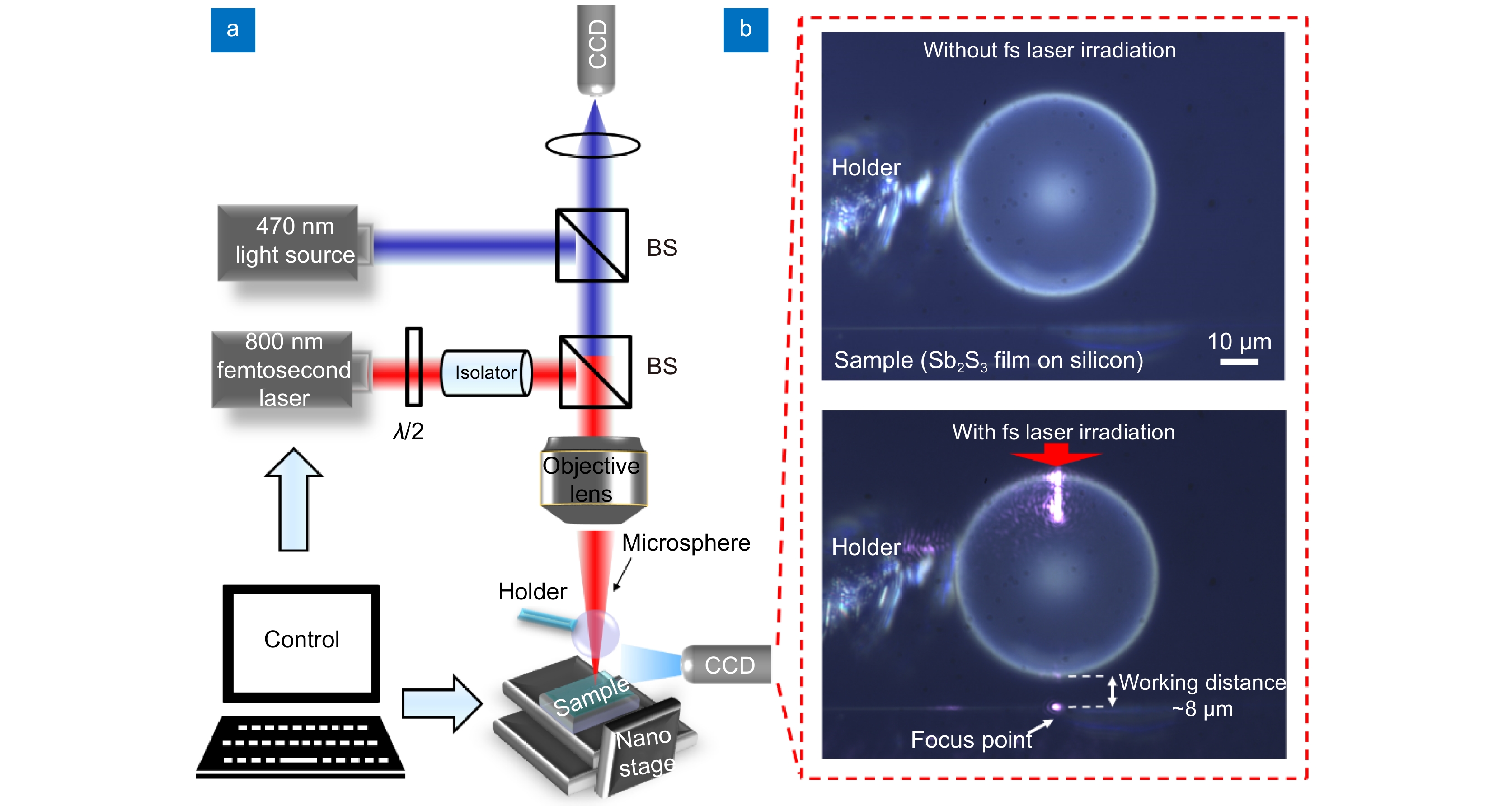
Figure 1.
(a) Experimental setup of non-contact microsphere femtosecond laser irradiation. (b) Side view of microsphere focusing with femtosecond laser beam.
-
Figure 2.
(a) SEM and (b) AFM images, as well as (c) corresponding cross-sectional profile of sub-50 nm nano-lines created at the laser fluence of 0.38 mJ/cm2 and scanning speed of 100 μm/s.
-
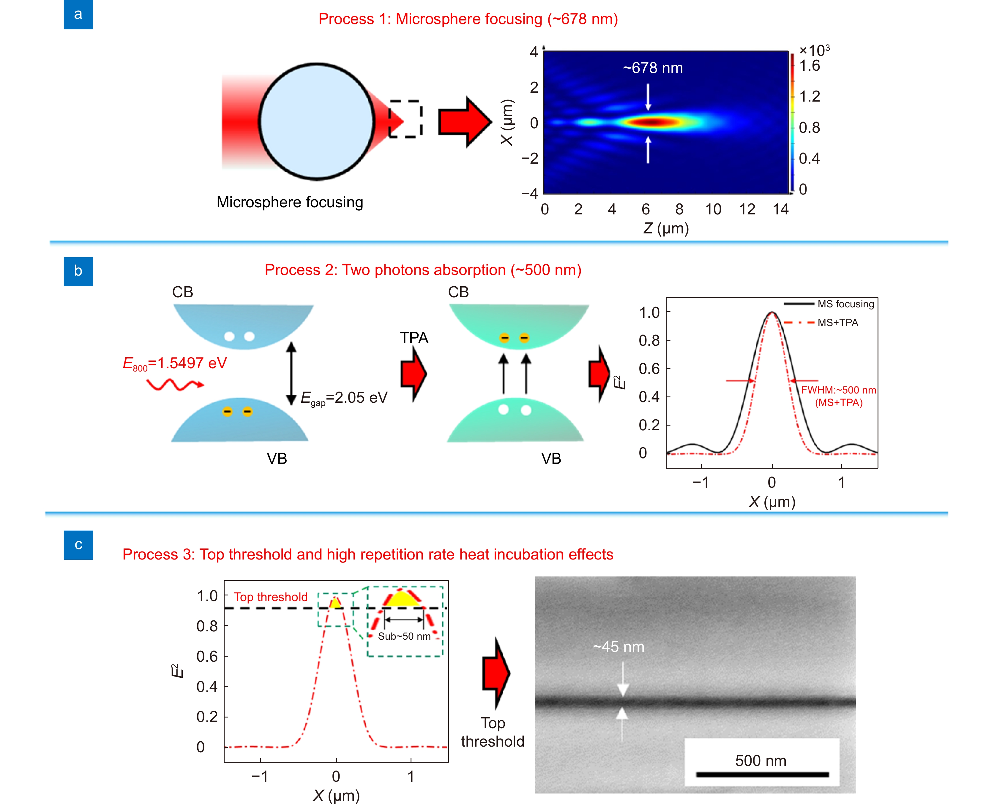
Figure 3.
Formation mechanism of microsphere femtosecond laser irradiation. (a) Focusing via 50 μm microsphere by 800 nm laser irradiation. (b) TPA of Sb2S3 thin films under 800 nm femtosecond laser irradiation. (c) top threshold and high-repetition-rate femtosecond laser induced incubation effects.
-
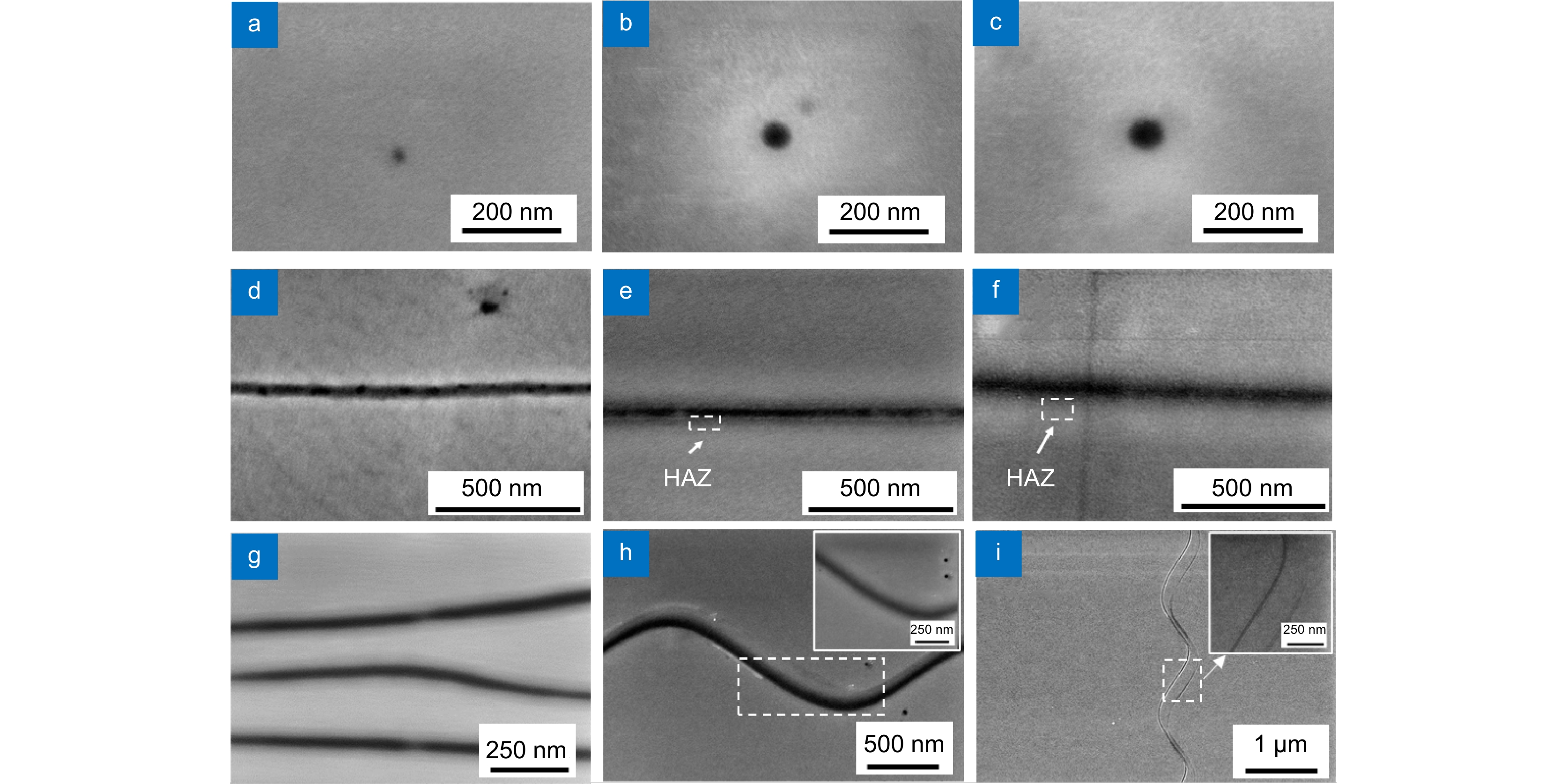
Figure 4.
Different nano-structures created by microsphere femtosecond laser irradiation on 30 nm thick Sb2S3 thin films. Nano-dots fabricated at different laser fluences of (a) 0.30, (b) 0.42, and (c) 0.46 mJ/cm2. Single nano-lines made at a scanning speed of 100 μm/s and different laser fluences of (d) 0.38, (e) 0.42, and (f) 0.46 mJ/cm2. Irradiation results of arbitrary structures. (g) Irregular sub-50 nm triple nano-lines, (h) single sub-100 nm, and (i) double sub-50 nm wavy nano-lines.
-
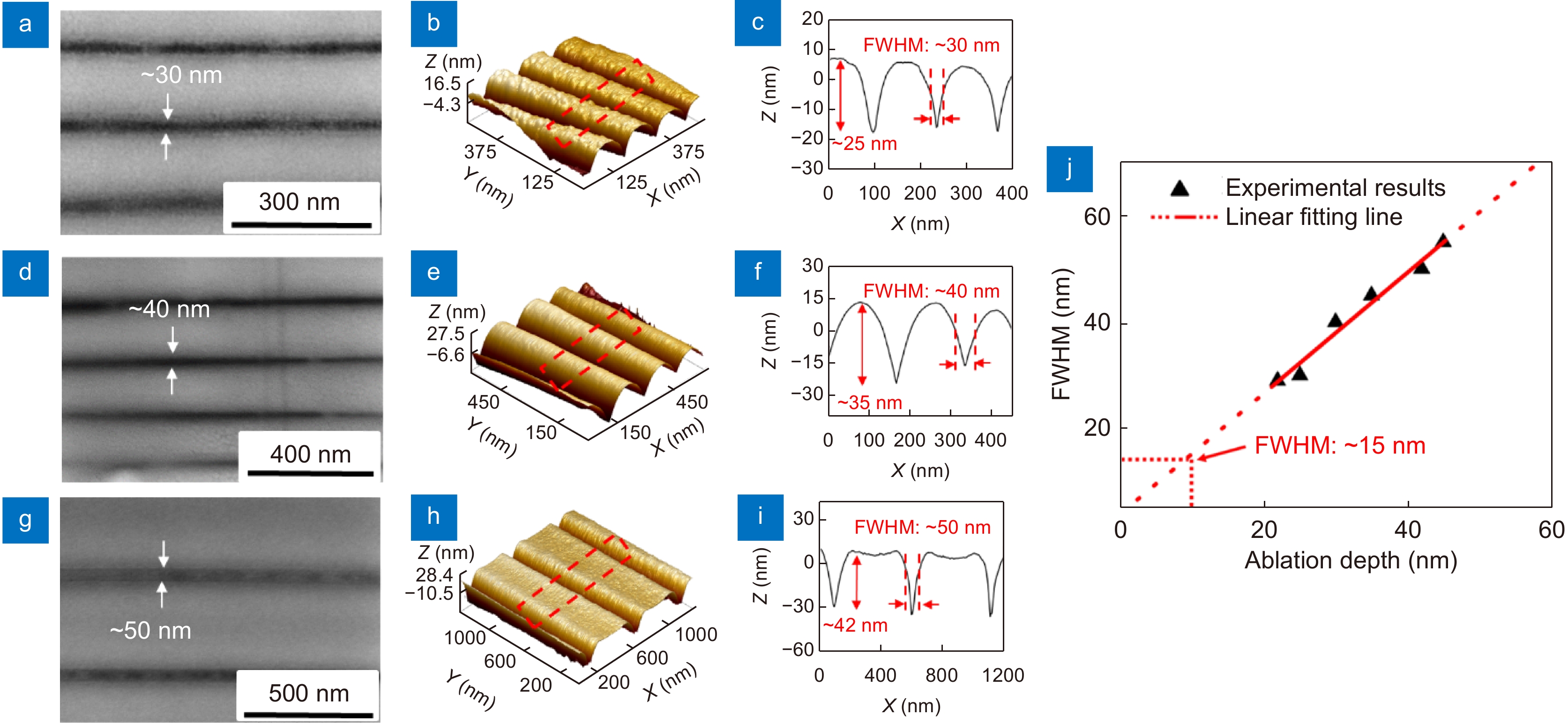
Figure 5.
SEM and AFM images of the nano-structures created on Sb2S3 thin films at the film thickness of (a–c) ~25, (d–f) ~35, and (g–i) ~42 nm. (j) Linear fitting analysis of the FWHM vs ablation depth.
-
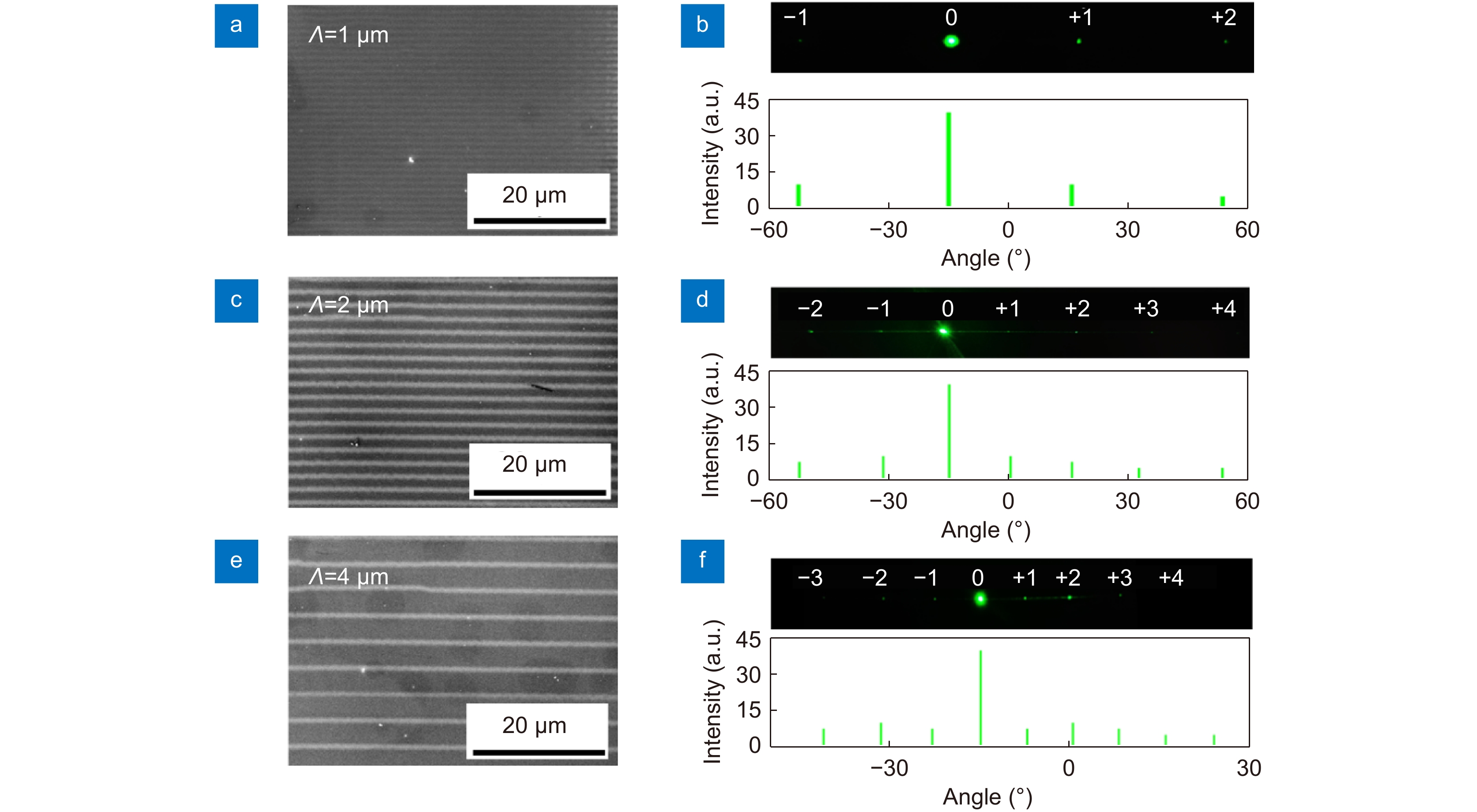
Figure 6.
SEM images of the reflective grating by microsphere femtosecond laser irradiation at a period of (a) 1, (c) 2, and (e) 4 μm, respectively. The diffraction pattern, diffraction intensity, and angle observed in reflection for grating structures at a period of (b) 1, (d) 2, and (f) 4 μm, respectively. The number refers to the diffraction order of each reflective grating.


