
 E-mail Alert
 RSS
RSS
| Citation: |
Li CH, Du W, Huang YX, Zou JH, Luo LZ et al. Photonic synapses with ultralow energy consumption for artificial visual perception and brain storage. Opto-Electron Adv 5, 210069 (2022). doi: 10.29026/oea.2022.210069

|
Photonic synapses with ultralow energy consumption for artificial visual perception and brain storage
-
Abstract
The human visual system, dependent on retinal cells, can be regarded as a complex combination of optical system and nervous system. Artificial retinal system could mimic the sensing and processing function of human eyes. Optically stimulated synaptic devices could serve as the building blocks for artificial retinas and subsequent information transmission system to brain. Herein, photonic synaptic transistors based on polycrystalline MoS2, which could simulate human visual perception and brain storage, are presented. Moreover, the photodetection range from visible light to near-infrared light of MoS2 multilayer could extend human eyes’ vision limitation to near-infrared light. Additionally, the photonic synaptic transistor shows an ultrafast speed within 5 μs and ultralow power consumption under optical stimuli about 40 aJ, several orders of magnitude lower than biological synapses (50 ms and 10 fJ). Furthermore, the backgate control could act as emotional modulation of the artificial brain to enhance or suppress memory function, i.e. the intensity of photoresponse. The proposed carrier trapping/detrapping as the main working mechanism is presented for the device. In addition, synaptic functionalities including short synaptic plasticity, long synaptic plasticity and paired-pulse facilitation could be successfully simulated based on the prepared device. Furthermore, the large difference between short synaptic plasticity and long synaptic plasticity reveals the better image pre-processing function of the prepared photonic synapses. The classical Pavlovian conditioning associated with the associative learning is successfully implemented as well. Therefore, the efficient and rich functionalities demonstrate the potential of the MoS2 synaptic device that integrates sensing-memory-preprocessing capabilities for realizing artificial neural networks with different emotions that mimic human retina and brain.-
Keywords:
- MoS2 synaptic transistors /
- visual perception /
- ultralow power consumption /
- memory
-

-
References
[1] Pan X, Jin TY, Gao J, Han C, Shi YM et al. Stimuli-enabled artificial synapses for neuromorphic perception: progress and perspectives. Small 16, 2001504 (2020). doi: 10.1002/smll.202001504 [2] Zhang QM, Yu HY, Barbiero M, Wang BK, Gu M. Artificial neural networks enabled by nanophotonics. Light Sci Appl 8, 42 (2019). doi: 10.1038/s41377-019-0151-0 [3] Zhang K, Meng DL, Bai FM, Zhai JY, Wang ZL. Photon-memristive system for logic calculation and nonvolatile photonic storage. Adv Funct Mater 30, 2002945 (2020). doi: 10.1002/adfm.202002945 [4] Wu ZH, Lu JK, Shi T, Zhao XL, Zhang XM et al. A habituation sensory nervous system with memristors. Adv Mater 32, 2004398 (2020). doi: 10.1002/adma.202004398 [5] Zhang JY, Dai SL, Zhao YW, Zhang JH, Huang J. Recent progress in photonic synapses for neuromorphic systems. Adv Intell Syst 2, 1900136 (2020). doi: 10.1002/aisy.201900136 [6] Zhang C, Wang SY, Zhao XL, Yang YH, Tong YH et al. Sub-femtojoule-energy-consumption conformable synaptic transistors based on organic single-crystalline nanoribbons. Adv Funct Mater 31, 2007894 (2021). doi: 10.1002/adfm.202007894 [7] Kumarasinghe K, Kasabov N, Taylor D. Brain-inspired spiking neural networks for decoding and understanding muscle activity and kinematics from electroencephalography signals during hand movements. Sci Rep 11, 2486 (2021). doi: 10.1038/s41598-021-81805-4 [8] Wang L, Liao WG, Wong SL, Yu ZG, Li SF et al. Artificial synapses based on multiterminal memtransistors for neuromorphic application. Adv Funct Mater 29, 1901106 (2019). doi: 10.1002/adfm.201901106 [9] Liu CS, Chen HW, Wang SY, Liu Q, Jiang YG et al. Two-dimensional materials for next-generation computing technologies. Nat Nanotechnol 15, 545–557 (2020). doi: 10.1038/s41565-020-0724-3 [10] Zuo HR, Xu ZY, Zhang JL, Jia G. Visual tracking based on transfer learning of deep salience information. Opto-Electron Adv 3, 190018 (2020). [11] Zhang L, Pan J, Zhang Z, Wu H, Yao N et al. Ultrasensitive skin-like wearable optical sensors based on glass micro/nanofibers. Opto-Electron Adv 3, 190022 (2020). [12] Cheng YC, Li HJW, Liu B, Jiang LY, Liu M et al. Vertical 0D-perovskite/2D-MoS2 van der Waals heterojunction phototransistor for emulating photoelectric-synergistically classical pavlovian conditioning and neural coding dynamics. Small 16, 2005217 (2020). doi: 10.1002/smll.202005217 [13] Tan ZH, Yin XB, Yang R, Mi SB, Jia CL et al. Pavlovian conditioning demonstrated with neuromorphic memristive devices. Sci Rep 7, 713 (2017). doi: 10.1038/s41598-017-00849-7 [14] Yin L, Huang W, Xiao RL, Peng WB, Zhu YY et al. Optically stimulated synaptic devices based on the hybrid structure of silicon nanomembrane and perovskite. Nano Lett 20, 3378–3387 (2020). doi: 10.1021/acs.nanolett.0c00298 [15] Ahmed T, Tahir M, Low MX, Ren YY, Tawfik SA et al. Fully light-controlled memory and neuromorphic computation in layered black phosphorus. Adv Mater 33, 2004207 (2021). doi: 10.1002/adma.202004207 [16] Gillick BT, Zirpel L. Neuroplasticity: an appreciation from synapse to system. Arch Phys Med Rehabil 93, 1846–1855 (2012). doi: 10.1016/j.apmr.2012.04.026 [17] Wang TY, Meng JL, He ZY, Chen L, Zhu H et al. Ultralow power wearable heterosynapse with photoelectric synergistic modulation. Adv Sci 7, 1903480 (2020). doi: 10.1002/advs.201903480 [18] Zhai YB, Zhou Y, Yang XQ, Wang F, Ye WB et al. Near infrared neuromorphic computing via upconversion-mediated optogenetics. Nano Energy 67, 104262 (2020). doi: 10.1016/j.nanoen.2019.104262 [19] Majumdar S, Tan HW, Qin QH, van Dijken S. Energy-efficient organic ferroelectric tunnel junction memristors for neuromorphic computing. Adv Electron Mater 5, 1800795 (2019). doi: 10.1002/aelm.201800795 [20] Hebb DO. The Organization of Behavior: A Neuropsychological Theory (Psychology Press, London, 2005). [21] Bear MF, Connors BW, Paradiso MA. Neuroscience Exploring the Brain (Lippincott Williams & Wilkins, Philadelphia, 2007). [22] Xiao ZG, Huang JS. Energy-efficient hybrid perovskite memristors and synaptic devices. Adv Electron Mater 2, 1600100 (2016). doi: 10.1002/aelm.201600100 [23] Ma FM, Zhu YB, Xu ZW, Liu Y, Zheng XJ et al. Optoelectronic perovskite synapses for neuromorphic computing. Adv Funct Mater 30, 1908901 (2020). doi: 10.1002/adfm.201908901 [24] Han H, Yu HY, Wei HH, Gong JD, Xu WT. Recent progress in three-terminal artificial synapses: from device to system. Small 15, 1900695 (2019). doi: 10.1002/smll.201900695 [25] Qian C, Oh S, Choi Y, Kim JH, Sun J et al. Solar-stimulated optoelectronic synapse based on organic heterojunction with linearly potentiated synaptic weight for neuromorphic computing. Nano Energy 66, 104095 (2019). doi: 10.1016/j.nanoen.2019.104095 [26] Berco D, Ang DS, Zhang HZ. An optoneuronic device with realistic retinal expressions for bioinspired machine vision. Adv Intell Syst 2, 1900115 (2020). doi: 10.1002/aisy.201900115 [27] Park HL, Kim H, Lim D, Zhou HY, Kim YH et al. Retina-inspired carbon nitride-based photonic synapses for selective detection of UV light. Adv Mater 32, 1906899 (2020). doi: 10.1002/adma.201906899 [28] Wei ZM, Li B, Xia CX, Cui Y, He J et al. Various structures of 2D transition-metal dichalcogenides and their applications. Small Methods 2, 1800094 (2018). doi: 10.1002/smtd.201800094 [29] Du W, Li CH, Sun JC, Xu H, Yu P et al. Nanolasers based on 2D materials. Laser Photonics Rev 14, 2000271 (2020). doi: 10.1002/lpor.202000271 [30] Zhao ZH, Wu D, Guo JW, Wu EP, Jia C et al. Synthesis of large-area 2D WS2 films and fabrication of a heterostructure for self-powered ultraviolet photodetection and imaging applications. J Mater Chem C 7, 12121–12126 (2019). doi: 10.1039/C9TC03866C [31] Zhang XM, Xiao SQ, Shi LH, Nan HY, Wan X et al. Large-size Mo1-xWxS2 and W1-xMoxS2 (x = 0–0.5) monolayers by confined-space chemical vapor deposition. Appl Surf Sci 457, 591–597 (2018). doi: 10.1016/j.apsusc.2018.06.299 [32] Akinwande D, Huyghebaert C, Wang CH, Serna MI, Goossens S et al. Graphene and two-dimensional materials for silicon technology. Nature 573, 507–518 (2019). doi: 10.1038/s41586-019-1573-9 [33] Fang MX, Wang F, Han YM, Feng YL, Ren TL et al. Controlled growth of bilayer-MoS2 films and MoS2-based field-effect transistor (FET) performance optimization. Adv Electron Mater 4, 1700524 (2018). doi: 10.1002/aelm.201700524 [34] Wu M, Xiao YH, Zeng Y, Zhou YL, Zeng XB et al. Synthesis of two-dimensional transition metal dichalcogenides for electronics and optoelectronics. InfoMat 3, 362–396 (2021). doi: 10.1002/inf2.12161 [35] Feng XW, Liu XK, Ang KW. 2D photonic memristor beyond graphene: progress and prospects. Nanophotonics 9, 1579–1599 (2020). doi: 10.1515/nanoph-2019-0543 [36] Li ZW, Yang W, Huang M, Yang X, Zhu CG et al. Light-triggered interfacial charge transfer and enhanced photodetection in CdSe/ZnS quantum dots/MoS2 mixed-dimensional phototransistors. Opto-Electron Adv 4, 210017 (2021). doi: 10.29026/oea.2021.210017 [37] Sup Choi M, Lee GH, Yu YJ, Lee DY, Hwan Lee S et al. Controlled charge trapping by molybdenum disulphide and graphene in ultrathin heterostructured memory devices. Nat Commun 4, 1624 (2013). doi: 10.1038/ncomms2652 [38] Hu YX, Dai MJ, Feng W, Zhang X, Zhang SC et al. Monolayer hydrophilic MoS2 with strong charge trapping for atomically thin neuromorphic vision systems. Mater Horiz 7, 3316–3324 (2020). doi: 10.1039/D0MH01472A [39] Huang W, Xia XW, Zhu C, Steichen P, Quan WD et al. Memristive artificial synapses for neuromorphic computing. Nano-Micro Lett 13, 85 (2021). doi: 10.1007/s40820-021-00618-2 [40] Gao CF, Lee MP, Li MJ, Lee KC, Yang FS et al. Mimic drug dosage modulation for neuroplasticity based on charge-trap layered electronics. Adv Funct Mater 31, 2005182 (2021). doi: 10.1002/adfm.202005182 [41] Choi C, Leem J, Kim MS, Taqieddin A, Cho C et al. Curved neuromorphic image sensor array using a MoS2-organic heterostructure inspired by the human visual recognition system. Nat Commun 11, 5934 (2020). doi: 10.1038/s41467-020-19806-6 [42] Qin SC, Wang FQ, Liu YJ, Wan Q, Wang XR et al. A light-stimulated synaptic device based on graphene hybrid phototransistor. 2D Mater 4, 035022 (2017). doi: 10.1088/2053-1583/aa805e [43] Kumar M, Abbas S, Kim J. All-oxide-based highly transparent photonic synapse for neuromorphic computing. ACS Appl Mater Interfaces 10, 34370–34376 (2018). doi: 10.1021/acsami.8b10870 [44] Chen TQ, Wang X, Hao DD, Dai SL, Ou QQ et al. Photonic synapses with ultra-low energy consumption based on vertical organic field-effect transistors. Adv Opt Mater 9, 2002030 (2021). doi: 10.1002/adom.202002030 [45] Xiao M, Wang HD, Liu JF, Yang H, Zhang H. Artificial visual memory device based on a photo-memorizing composite and one-step manufacturing. Mater Horiz 7, 1597–1604 (2020). doi: 10.1039/D0MH00312C [46] Zhu JT, Li W, Huang R, Ma L, Sun HM et al. One-pot selective epitaxial growth of large WS2/MoS2 lateral and vertical heterostructures. J Am Chem Soc 142, 16276–16284 (2020). doi: 10.1021/jacs.0c05691 [47] Ganger ZD. Growth of two-dimensional molybdenum disulfide via chemical vapor deposition (Wright State University, Dayton, 2019). [48] Hong S, Zagni N, Choo S, Liu N, Baek S et al. Highly sensitive active pixel image sensor array driven by large-area bilayer MoS2 transistor circuitry. Nat Commun 12, 3559 (2021). doi: 10.1038/s41467-021-23711-x [49] Lee HS, Min SW, Chang YG, Park MK, Nam T et al. MoS2 nanosheet phototransistors with thickness-modulated optical energy gap. Nano Lett 12, 3695–3700 (2012). doi: 10.1021/nl301485q [50] Choi W, Cho MY, Konar A, Lee JH, Cha GB et al. High-detectivity multilayer MoS2 phototransistors with spectral response from ultraviolet to infrared. Adv Mater 24, 5832–5836 (2012). doi: 10.1002/adma.201201909 [51] Ren AB, Zou JH, Lai HG, Huang YX, Yuan LM et al. Direct laser-patterned MXene–perovskite image sensor arrays for visible-near infrared photodetection. Mater Horiz 7, 1901–1911 (2020). doi: 10.1039/D0MH00537A [52] Yang ZB, Hao JH, Lau SP. Synthesis, properties, and applications of 2D amorphous inorganic materials. J Appl Phys 127, 220901 (2020). doi: 10.1063/1.5144626 [53] Bittle EG, Basham JI, Jackson TN, Jurchescu OD, Gundlach DJ. Mobility overestimation due to gated contacts in organic field-effect transistors. Nat Commun 7, 10908 (2016). doi: 10.1038/ncomms10908 [54] Fashandi H, Dahlqvist M, Lu J, Palisaitis J, Simak SI et al. Synthesis of Ti3AuC2, Ti3Au2C2 and Ti3IrC2 by noble metal substitution reaction in Ti3SiC2 for high-temperature-stable Ohmic contacts to SiC. Nat Mater 16, 814–818 (2017). doi: 10.1038/nmat4896 [55] Wang Y, Kim JC, Wu RJ, Martinez J, Song XJ et al. Van der Waals contacts between three-dimensional metals and two-dimensional semiconductors. Nature 568, 70–74 (2019). doi: 10.1038/s41586-019-1052-3 [56] Shen PC, Su C, Lin YX, Chou AS, Cheng CC et al. Ultralow contact resistance between semimetal and monolayer semiconductors. Nature 593, 211–217 (2021). doi: 10.1038/s41586-021-03472-9 [57] Zhou FC, Chen JW, Tao XM, Wang XR, Chai Y. 2D materials based optoelectronic memory: convergence of electronic memory and optical sensor. Research 2019, 9490413 (2019). [58] Jonsson A, Sjöström TA, Tybrandt K, Berggren M, Simon DT. Chemical delivery array with millisecond neurotransmitter release. Sci Adv 2, e1601340 (2016). doi: 10.1126/sciadv.1601340 [59] Hao DD, Zhang JY, Dai SL, Zhang JH, Huang J. Perovskite/organic semiconductor-based photonic synaptic transistor for artificial visual system. ACS Appl Mater Interfaces 12, 39487–39495 (2020). doi: 10.1021/acsami.0c10851 [60] Tu LQ, Cao RR, Wang XD, Chen Y, Wu SQ et al. Ultrasensitive negative capacitance phototransistors. Nat Commun 11, 101 (2020). doi: 10.1038/s41467-019-13769-z [61] Wang X, Lu Y, Zhang JY, Zhang SQ, Chen TQ et al. Highly sensitive artificial visual array using transistors based on porphyrins and semiconductors. Small 17, 2005491 (2021). doi: 10.1002/smll.202005491 [62] Meng Y, Li FZ, Lan CY, Bu XM, Kang XL et al. Artificial visual systems enabled by quasi–two-dimensional electron gases in oxide superlattice nanowires. Sci Adv 6, eabc6389 (2020). doi: 10.1126/sciadv.abc6389 [63] Wang Y, Lv ZY, Chen JR, Wang ZP, Zhou Y et al. Photonic synapses based on inorganic perovskite quantum dots for neuromorphic computing. Adv Mater 30, 1802883 (2018). doi: 10.1002/adma.201802883 [64] Ahmed T, Kuriakose S, Mayes ELH, Ramanathan R, Bansal V et al. Optically stimulated artificial synapse based on layered black phosphorus. Small 15, 1900966 (2019). doi: 10.1002/smll.201900966 [65] Pradhan B, Das S, Li JX, Chowdhury F, Cherusseri J et al. Ultrasensitive and ultrathin phototransistors and photonic synapses using perovskite quantum dots grown from graphene lattice. Sci Adv 6, eaay5225 (2020). doi: 10.1126/sciadv.aay5225 [66] Jiang J, Hu WN, Xie DD, Yang JL, He J et al. 2D electric-double-layer phototransistor for photoelectronic and spatiotemporal hybrid neuromorphic integration. Nanoscale 11, 1360–1369 (2019). doi: 10.1039/C8NR07133K [67] Wang SY, Chen CS, Yu ZH, He YL, Chen XY et al. A MoS2/PTCDA hybrid heterojunction synapse with efficient photoelectric dual modulation and versatility. Adv Mater 31, 1806227 (2019). doi: 10.1002/adma.201806227 [68] Cheng ZG, Ríos C, Pernice WHP, Wright CD, Bhaskaran H. On-chip photonic synapse. Sci Adv 3, e1700160 (2017). doi: 10.1126/sciadv.1700160 [69] Zhao YY, Sun WJ, Wang J, He JH, Li H et al. All-inorganic ionic polymer-based memristor for high-performance and flexible artificial synapse. Adv Funct Mater 30, 2004245 (2020). doi: 10.1002/adfm.202004245 [70] Wang K, Dai SL, Zhao YW, Wang Y, Liu C et al. Light-stimulated synaptic transistors fabricated by a facile solution process based on inorganic perovskite quantum dots and organic semiconductors. Small 15, 1900010 (2019). doi: 10.1002/smll.201900010 [71] Kufer D, Konstantatos G. Highly sensitive, encapsulated MoS2 photodetector with gate controllable gain and speed. Nano Lett 15, 7307–7313 (2015). doi: 10.1021/acs.nanolett.5b02559 [72] Zhao QH, Wang W, Carrascoso-Plana F, Jie WQ, Wang T et al. The role of traps in the photocurrent generation mechanism in thin InSe photodetectors. Mater Horiz 7, 252–262 (2020). doi: 10.1039/C9MH01020C [73] Guo JM, Wen RM, Zhai JY, Wang ZL. Enhanced NO2 gas sensing of a single-layer MoS2 by photogating and piezo-phototronic effects. Sci Bull 64, 128–135 (2019). doi: 10.1016/j.scib.2018.12.009 [74] Zhao XN, Xu HY, Wang ZQ, Lin Y, Liu YC. Memristors with organic-inorganic halide perovskites. InfoMat 1, 183–210 (2019). [75] Zucker RS, Regehr WG. Short-term synaptic plasticity. Annu Rev Physiol 64, 355–405 (2002). doi: 10.1146/annurev.physiol.64.092501.114547 [76] Lee KC, Li MJ, Chang YH, Yang SH, Lin CY et al. Inverse paired-pulse facilitation in neuroplasticity based on interface-boosted charge trapping layered electronics. Nano Energy 77, 105258 (2020). doi: 10.1016/j.nanoen.2020.105258 [77] Simmons JG, Taylor GW. Nonequilibrium steady-state statistics and associated effects for insulators and semiconductors containing an arbitrary distribution of traps. Phys Rev B 4, 502–511 (1971). doi: 10.1103/PhysRevB.4.502 [78] Jiang J, Ling CY, Xu T, Wang WH, Niu XH et al. Defect engineering for modulating the trap states in 2D photoconductors. Adv Mater 30, 1804332 (2018). doi: 10.1002/adma.201804332 [79] Ebbinghaus H. Über das Gedächtnis: Untersuchungen zur Experimentellen Psychologie (Duncker & Humber, Leipzig, 1885). [80] Laborieux A, Ernoult M, Hirtzlin T, Querlioz D. Synaptic metaplasticity in binarized neural networks. Nat Commun 12, 2549 (2021). doi: 10.1038/s41467-021-22768-y [81] Wang Y, Yin L, Huang W, Li YY, Huang SJ et al. Optoelectronic synaptic devices for neuromorphic computing. Adv Intell Syst 3, 2000099 (2021). doi: 10.1002/aisy.202000099 [82] Loftus GR. Evaluating forgetting curves. J Exp Psychol Learn Mem Cogn 11, 397–406 (1985). doi: 10.1037/0278-7393.11.2.397 [83] Zhang ZZ, Wang ZW, Shi T, Bi C, Rao F et al. Memory materials and devices: from concept to application. InfoMat 2, 261–290 (2020). doi: 10.1002/inf2.12077 [84] Rolls ET, Stringer SM. A model of the interaction between mood and memory. Netw Comput Neural Syst 12, 89–109 (2001). doi: 10.1080/net.12.2.89.109 [85] Bryan T, Mathur S, Sullivan K. The impact of positive mood on learning. Learn Disabil Quart 19, 153–162 (1996). doi: 10.2307/1511058 [86] Zou JY, Cai ZY, Lai YJ, Tan JY, Zhang RJ et al. Doping concentration modulation in vanadium-doped monolayer molybdenum disulfide for synaptic transistors. ACS Nano 15, 7340–7347 (2021). doi: 10.1021/acsnano.1c00596 [87] Wang SY, Liu L, Gan LR, Chen HW, Hou X et al. Two-dimensional ferroelectric channel transistors integrating ultra-fast memory and neural computing. Nat Commun 12, 53 (2021). doi: 10.1038/s41467-020-20257-2 -
Access History
Figures(6)
Article Metrics

Export File
Citation
Li CH, Du W, Huang YX, Zou JH, Luo LZ et al. Photonic synapses with ultralow energy consumption for artificial visual perception and brain storage. Opto-Electron Adv 5, 210069 (2022). doi: 10.29026/oea.2022.210069
Format
Content
 DownLoad:


-
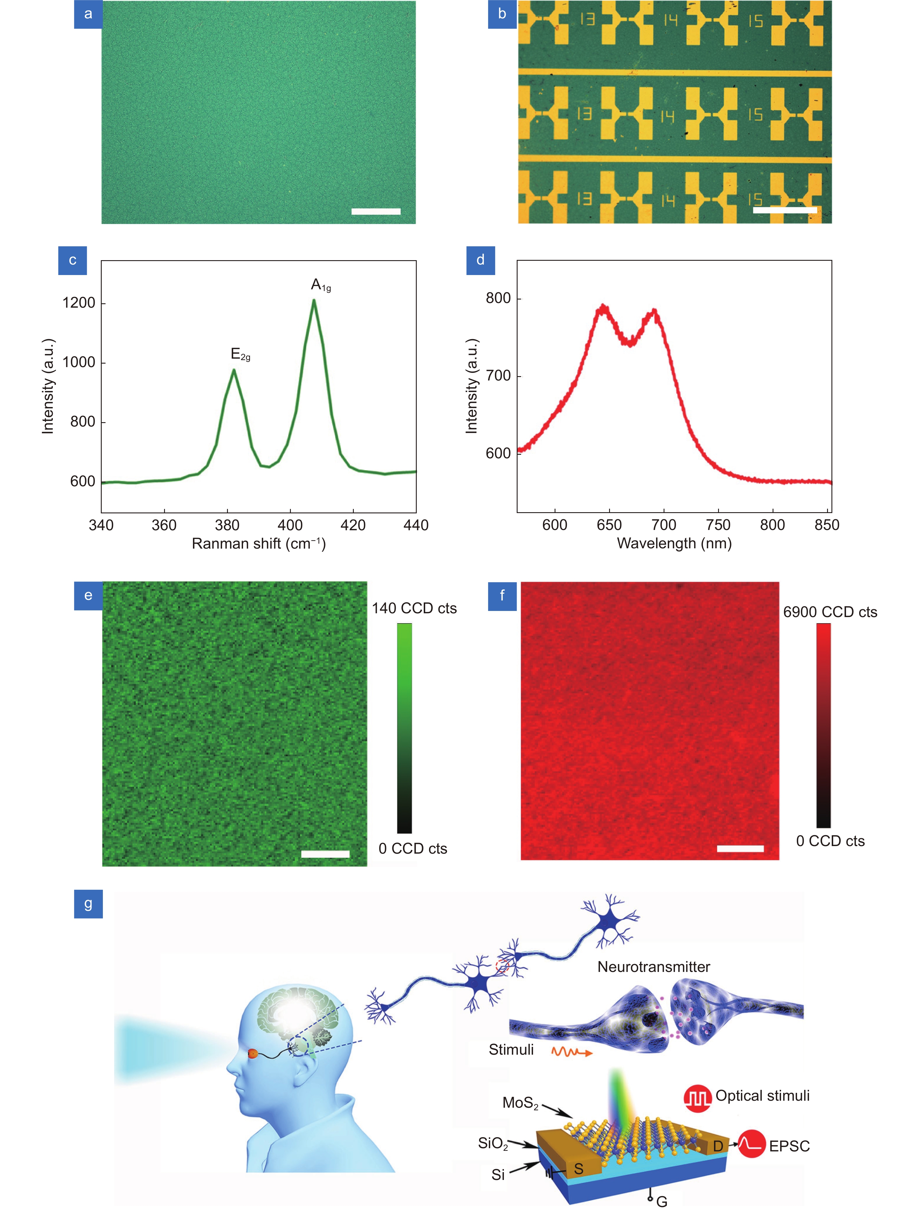
Figure 1.
Optical characterizations of MoS2 synaptic transistors and schematic diagram of human eyes. (a) The optical image of large-area and uniform polycrystalline MoS2. Scale bar: 100 μm. (b) The optical photograph of a MoS2 synaptic transistor array on Si/SiO2 substrate. Scale bar: 500 μm. The corrsponding Raman spectrum (c) and PL spectrum (d) of MoS2. The corresponding Raman mapping around 381.4 cm–1 (e) and PL mapping (f) selected randomly from (a). Scale bar: 8 μm. (g) Schematic diagram of visual perception and information transmission in human brain and corresponding artifical MoS2 synaptic device.
-
Figure 2.
Photodetection and spike-duration plasticity of the MoS2 synaptic transistor. Output characteristic curves of the MoS2 synaptic transistor in visible light (a) and NIR light (b). The inset in (b) is the corresponding linear output characteristic curve. (c) The transient current responses triggered by several optical stimulus with different duration of a single pulse, respectively. (d) The EPSC at the pulse width of 5 μs (405 nm, Vds = 1 V). (e) Comparison of single optical pulse width and power consumption among some synaptic devices.
-
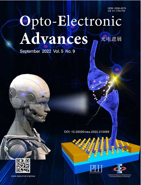
Figure 3.
STP characteristics of the MoS2 synaptic transistor. (a) The transient current response induced by an optical pulse of 50 ms. (b) The EPSC curves under different laser power densities (pulse width: 100 ms). Inset: The dependence of EPSC with differnent laser power densities (P). (c) The instantaneous current responses triggered by a pair of optical pulses (pulse width = 50 ms, pulse interval Δt = 2 s). The black dashed line represents the initial current in (a) and (c) without optical stimuli. (d) The PPF behaviors at different Δt.
-
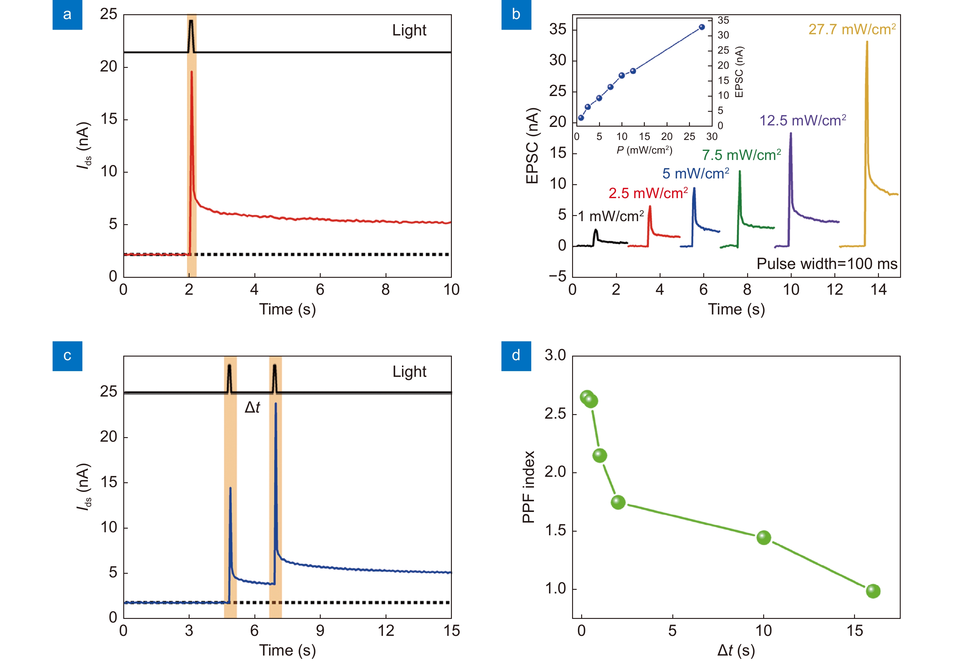
Figure 4.
LTP characteristics of the MoS2 synaptic transistor. The transient current (a), EPSC (b) and the extracted forgetting curve (c) from (a) after 10, 25, 50, 75 and 100 optical pulses. The transient current (d), A30/A1 (e) and the extracted forgetting curve (f) from (d) triggered by different spike frequency where A30 means the thirtieth EPSC. The black dashed line represents the initial current in (c) and (f) without optical stimuli.
-
Figure 5.
Schematic illustration of the Pavlovian conditioning and emotional effect on the MoS2 synaptic transistor. The classical Pavlovian conditioning under one training (E+L) (a) and ten trainings (b). (c) The transient current triggered by 30 optical spikes at the backgate of 0.1 V, 0 V and –0.1 V. (d) The maximum EPSC at different Vg.
-
Figure 6.
Neuromorphic imaging simulation. (a) Illustration of neuromorphic letter recognition. The stimulated letter recognition under STP (b), LTP with (c) or without (d) -Vg.


