
 E-mail Alert
 RSS
RSS
| Citation: |
Qi HX, Du ZC, Hu XY, Yang JY, Chu SS et al. High performance integrated photonic circuit based on inverse design method. Opto-Electron Adv 5, 210061 (2022). doi: 10.29026/oea.2022.210061

|
High performance integrated photonic circuit based on inverse design method
-
Abstract
The basic indexes of all-optical integrated photonic circuits include high-density integration, ultrafast response and ultra-low energy consumption. Traditional methods mainly adopt conventional micro/nano-structures. The overall size of the circuit is large, usually reaches hundreds of microns. Besides, it is difficult to balance the ultrafast response and ultra-low energy consumption problem, and the crosstalk between two traditional devices is difficult to overcome. Here, we propose and experimentally demonstrate an approach based on inverse design method to realize a high-density, ultrafast and ultra-low energy consumption integrated photonic circuit with two all-optical switches controlling the input states of an all-optical XOR logic gate. The feature size of the whole circuit is only 2.5 μm × 7 μm, and that of a single device is 2 μm × 2 μm. The distance between two adjacent devices is as small as 1.5 μm, within wavelength magnitude scale. Theoretical response time of the circuit is 150 fs, and the threshold energy is within 10 fJ/bit. We have also considered the crosstalk problem. The circuit also realizes a function of identifying two-digit logic signal results. Our work provides a new idea for the design of ultrafast, ultra-low energy consumption all-optical devices and the implementation of high-density photonic integrated circuits. -

-
References
[1] Floyd R, Hussain K, Mamun A, Gaevski M, Simin G et al. Photonics integrated circuits using AlxGa1-xN based UVC light-emitting diodes, photodetectors and waveguides. Appl Phys Express 13, 022003 (2020). doi: 10.7567/1882-0786/ab6410 [2] Zilkie AJ, Srinivasan P, Trita A, Schrans T, Yu GM et al. Multi-micron silicon photonics platform for highly manufacturable and versatile photonic integrated circuits. IEEE J Sel Top Quant Electron 25, 8200713 (2019). [3] Absil PP, Verheyen P, De Heyn P, Pantouvaki M, Lepage G et al. Silicon photonics integrated circuits: a manufacturing platform for high density, low power optical I/O’s. Opt Express 23, 9369–9378 (2015). doi: 10.1364/OE.23.009369 [4] Burgos CMV, Vamivakas N. Challenges in the path toward a scalable silicon photonics implementation of deep neural networks. IEEE J Quantum Electron 55, 8400110 (2019). [5] Feldmann J, Youngblood N, Karpov M, Gehring H, Li X et al. Parallel convolutional processing using an integrated photonic tensor core. Nature 589, 52–58 (2021). doi: 10.1038/s41586-020-03070-1 [6] Hegde RS. Photonics inverse design: pairing deep neural networks with evolutionary algorithms. IEEE J Sel Top Quant 26, 7700908 (2020). [7] Fathololoumi S, Hui D, Jadhav S, Chen J, Nguyen K et al. 1.6 Tbps silicon photonics integrated circuit and 800 Gbps photonic engine for switch co-packaging demonstration. J Lightwave Technol 39, 1155–1161 (2021). doi: 10.1109/JLT.2020.3039218 [8] Brodutch A, Marchildon R, Helmy AS. Dynamically reconfigurable sources for arbitrary Gaussian states in integrated photonics circuits. Opt Express 26, 17635–17648 (2018). doi: 10.1364/OE.26.017635 [9] Naweed A. Photonic coherence effects from dual-waveguide coupled pair of co-resonant microring resonators. Opt Express 23, 12573–12581 (2015). doi: 10.1364/OE.23.012573 [10] Zhang ZC, Ng GI, Hu T, Qiu HD, Guo X et al. Electromagnetically induced transparency-like effect in microring-Bragg gratings based coupling resonant system. Opt Express 24, 25665–25675 (2016). doi: 10.1364/OE.24.025665 [11] Azizpour MRJ, Soroosh M, Dalvand N, Seifi-Kavian Y. All-optical ultra-fast graphene-photonic crystal switch. Crystals 9, 461 (2019). doi: 10.3390/cryst9090461 [12] Zhang L, Sun YH, Li ZJ, Wang L, Cao SQ et al. Photonic crystal based on mott phase change material as all-optical bandgap switch and composite logic gate. Opt Mater 113, 110855 (2021). doi: 10.1016/j.optmat.2021.110855 [13] Chai Z, Hu XY, Yang H, Gong QH. All-optical tunable on-chip plasmon-induced transparency based on two surface-plasmon-polaritons absorption. Appl Phys Lett 108, 151104 (2016). doi: 10.1063/1.4946763 [14] Rutckaia V, Schilling J. Ultrafast low-energy all-optical switching. Nat Photonics 14, 4–6 (2020). doi: 10.1038/s41566-019-0571-7 [15] Davis TJ, Gómez DE, Eftekhari F. All-optical modulation and switching by a metamaterial of plasmonic circuits. Opt Lett 39, 4938–4941 (2014). doi: 10.1364/OL.39.004938 [16] Lotfi F, Sang-Nourpour N, Kheradmand R. Plasmonic all-optical switching based on metamaterial/metal waveguides with local nonlinearity. Nanotechnology 31, 015201 (2020). doi: 10.1088/1361-6528/ab44fc [17] Chai Z, Hu XY, Wang FF, Li C, Ao YT et al. Ultrafast on-chip remotely-triggered all-optical switching based on epsilon-near-zero nanocomposites. Laser Photonics Rev 11, 1700042 (2017). doi: 10.1002/lpor.201700042 [18] Pitris S, Mitsolidou C, Moralis-Pegios M, Alexoudi T, Pleros N. Crosstalk-aware wavelength-switched all-to-all optical interconnect using sub-optimal AWGRs. IEEE Photonics Technol Lett 31, 1507–1510 (2019). doi: 10.1109/LPT.2019.2935497 [19] Seyedi MA, Descos A, Chen CH, Fiorentino M, Penkler D et al. Crosstalk analysis of ring resonator switches for all-optical routing. Opt Express 24, 11668–11676 (2016). doi: 10.1364/OE.24.011668 [20] Michaels A, Yablonovitch E. Inverse design of near unity efficiency perfectly vertical grating couplers. Opt Express 26, 4766–4779 (2018). doi: 10.1364/OE.26.004766 [21] Piggott AY, Lu J, Babinec TM, Lagoudakis KG, Petykiewicz J et al. Inverse design and implementation of a wavelength demultiplexing grating coupler. Sci Rep 4, 7210 (2014). [22] Sun P, Van Vaerenbergh T, Fiorentino M, Beausoleil R. Adjoint-method-inspired grating couplers for CWDM O-band applications. Opt Express 28, 3756–3767 (2020). doi: 10.1364/OE.382986 [23] Piggott AY, Lu J, Lagoudakis KG, Petykiewicz J, Babinec TM et al. Inverse design and demonstration of a compact and broadband on-chip wavelength demultiplexer. Nat Photonics 9, 374–377 (2015). doi: 10.1038/nphoton.2015.69 [24] Su LG, Piggott AY, Sapra NV, Petykiewicz J, Vučković J. Inverse design and demonstration of a compact on-chip narrowband three-channel wavelength demultiplexer. ACS Photonics 5, 301–305 (2018). doi: 10.1021/acsphotonics.7b00987 [25] Chang WJ, Ren XS, Ao YQ, Lu LH, Cheng MF. Inverse design and demonstration of an ultracompact broadband dual-mode 3 dB power splitter. Opt Express 26, 24135–24144 (2018). doi: 10.1364/OE.26.024135 [26] Ma HS, Huang J, Zhang KW, Yang JB. Arbitrary-direction, multichannel and ultra-compact power splitters by inverse design method. Opt Commun 462, 125329 (2020). doi: 10.1016/j.optcom.2020.125329 [27] Chang WJ, Xu SY, Cheng MF, Liu DM, Zhang MM. Inverse design of a single-step-etched ultracompact silicon polarization rotator. Opt Express 28, 28343–28351 (2020). doi: 10.1364/OE.399052 [28] Lu QC, Wei W, Yan X, Shen B, Luo YB et al. Particle swarm optimized ultra-compact polarization beam splitter on silicon-on-insulator. Photonic Nanostruct Fundam Appl 32, 19–23 (2018). doi: 10.1016/j.photonics.2018.08.006 [29] Mirotznik MS, Prather DW, Mait JN, Beck WA, Shi SY et al. Three-dimensional analysis of subwavelength diffractive optical elements with the finite-difference time-domain method. Appl Opt 39, 2871–2880 (2000). doi: 10.1364/AO.39.002871 [30] Shi SY, Tao XD, Yang LQ, Prather DW. Analysis of diffractive optical elements using a nonuniform finite-difference time-domain method. Opt Eng 40, 503–510 (2001). doi: 10.1117/1.1355252 [31] Hughes TW, Minkov M, Williamson IAD, Fan SH. Adjoint method and inverse design for nonlinear nanophotonic devices. ACS Photonics 5, 4781–4787 (2018). doi: 10.1021/acsphotonics.8b01522 [32] Wang KY, Ren XS, Chang WJ, Lu LH, Liu DM et al. Inverse design of digital nanophotonic devices using the adjoint method. Photonics Res 8, 528–533 (2020). doi: 10.1364/PRJ.383887 [33] Deng Y, Ren SM, Fan KB, Malof JM, Padilla WJ. Neural-adjoint method for the inverse design of all-dielectric metasurfaces. Opt Express 29, 7526–7534 (2021). doi: 10.1364/OE.419138 -
Supplementary Information
Supplementary information for High performance integrated photonic circuit based on inverse design method 
-
Access History

Figures(7)
Tables(2)
Article Metrics


Export File
Citation
Qi HX, Du ZC, Hu XY, Yang JY, Chu SS et al. High performance integrated photonic circuit based on inverse design method. Opto-Electron Adv 5, 210061 (2022). doi: 10.29026/oea.2022.210061
Format
Content
 DownLoad:


-
Figure 1.
Design optimization process of the all-optical switch. (a) General configuration of the all-optical switch. (b) The initialization and discrete optimization permittivity distribution in the x-y two-dimensional cross-section, where bias=0 and bias=infinity.
-
Figure 2.
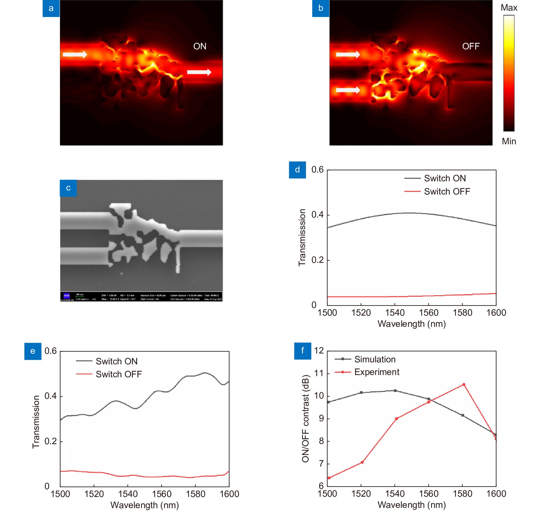
Characterization of the all-optical switch. (a) The “ON” state of normalized intensity distribution in the x-y plane from theoretical calculation. (b) The “OFF” state of normalized intensity distribution in the x-y plane from theoretical calculation. (c) Scanning electron microscopy (SEM) image of the all-optical switch. The size of the optimized area was 2 μm×2 μm. (d) Simulation results of the transmission of all-optical switch. (e) Experiment results of the normalized transmission of all-optical switch. (f) The simulation and experiment results of the all-optical switch ON/OFF contrast.
-
Figure 3.
Characterization of the all-optical switch. (a) The “OFF” state of normalized intensity distribution in the x-y plane from theoretical calculation at t=0 fs. (b–d) The “ON” state of normalized intensity distribution in the x-y plane from theoretical calculation at t=40 fs, 80 fs and 100 fs, respectively. (e) Transmission of the output of the all-optical switch under different delay time at 1500 nm-1600 nm. (f) Transmission of the output of the all-optical switch under different delay time at 1500 nm.
-
Figure 4.
Design optimization process of all-optical XOR logic gate. (a) General configuration of the all-optical XOR logic gate. (b) The initialization and discrete optimization permittivity distribution in the x-y two-dimensional cross-section, where bias=0 and bias=infinity.
-
Figure 5.
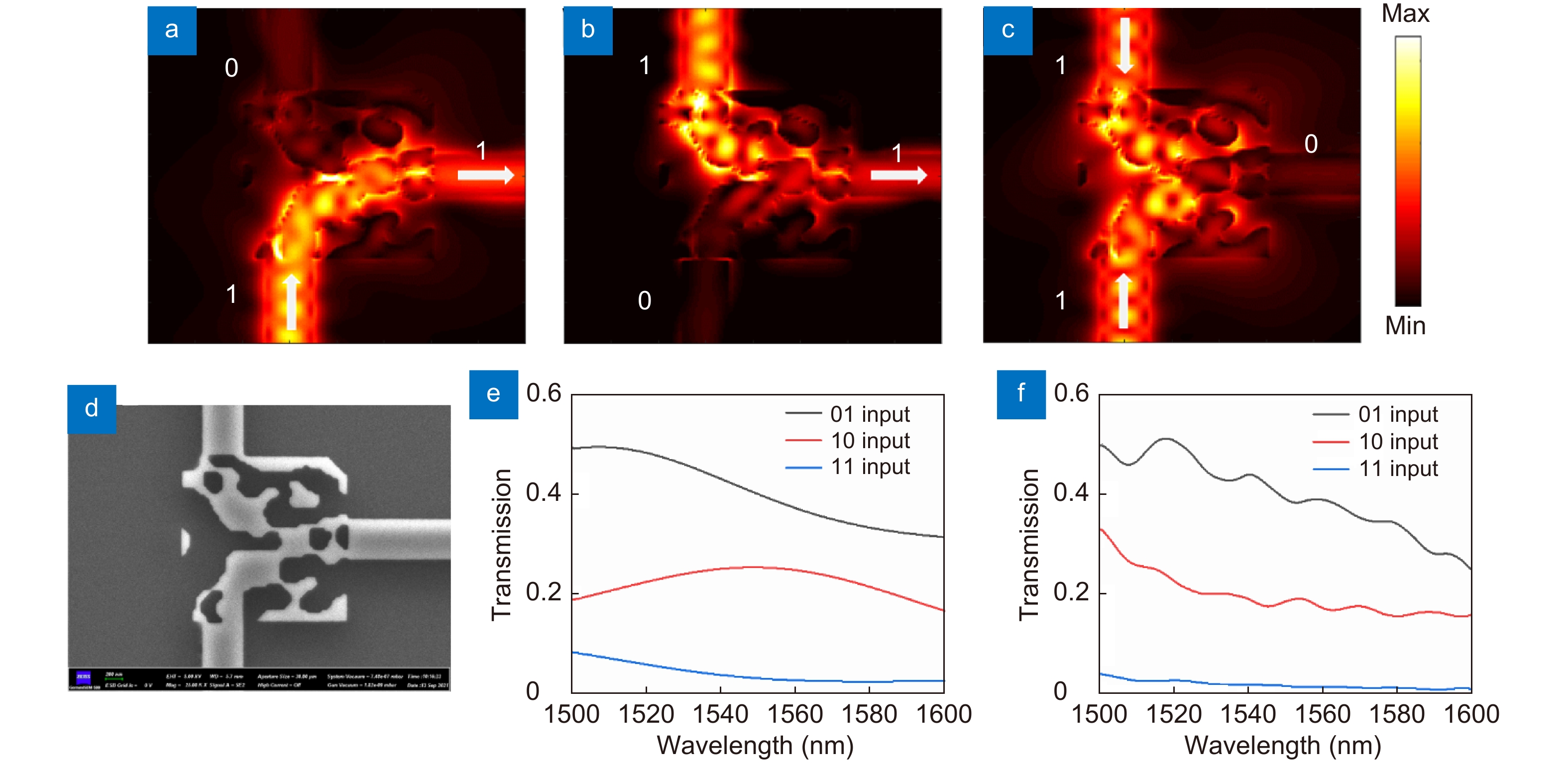
Characterization of the all-optical XOR logic gate. (a) The “01” input of normalized intensity distribution in the x-y plane from theoretical calculation. (b) The “10” input of normalized intensity distribution in the x-y plane from theoretical calculation. (c) The “11” input of normalized intensity distribution in the x-y plane from theoretical calculation. (d) Scanning electron microscopy (SEM)image of the XOR logic gate. The size of the optimized area was 2 μm×2 μm. (e) Simulation results of the transmission of all-optical switch. (f) Experiment results of the normalized transmission of all-optical XOR logic gate.
-
Figure 6.
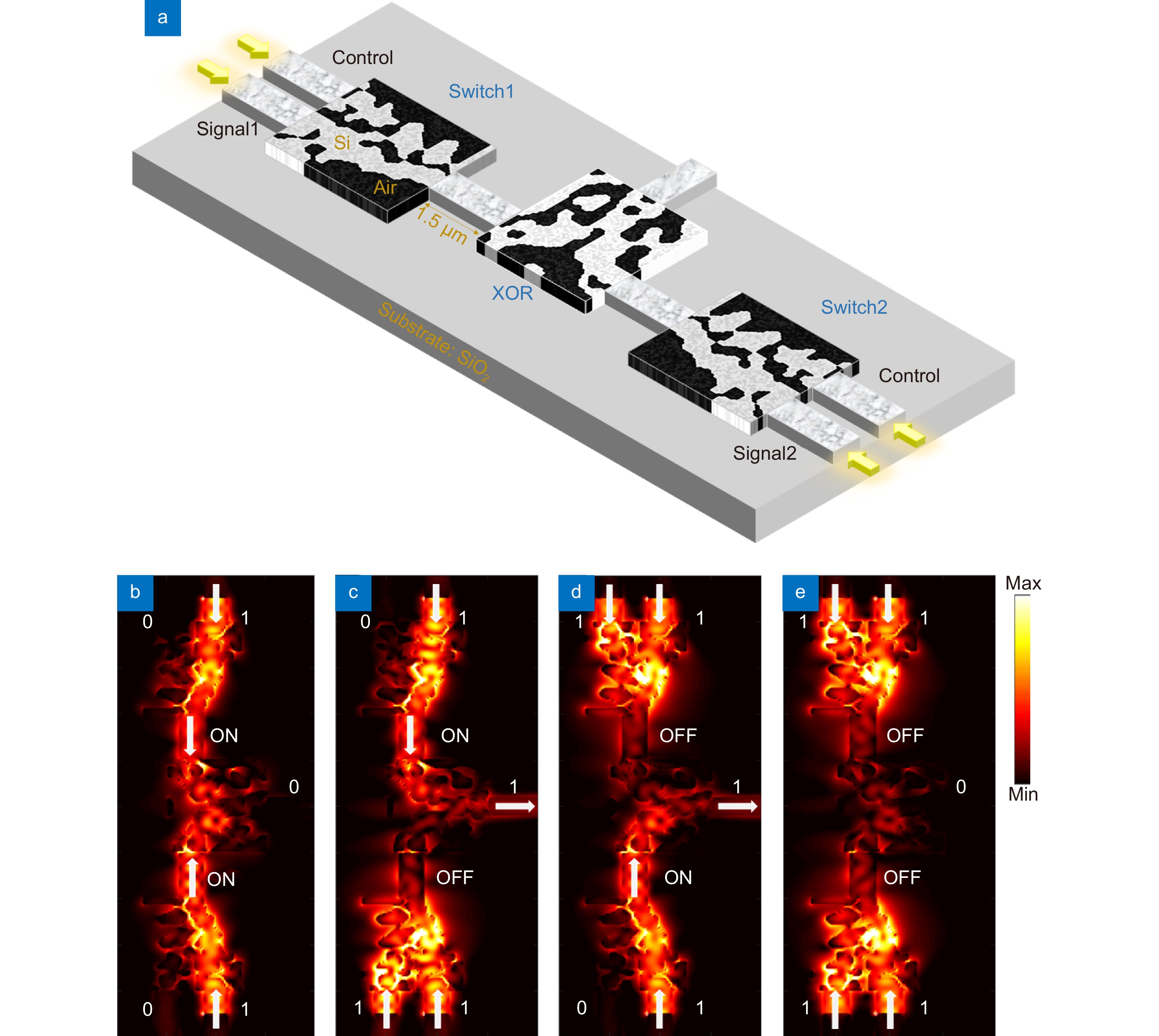
Characterization of the all-optical integrated circuit. (a) General configuration of the all-optical integrated circuit. (b) The “11” input (“ON” and ”ON” states) of normalized intensity distribution in the x-y plane from theoretical calculation. (c) The “10” input (“ON” and ”OFF” states) of normalized intensity distribution in the x-y plane from theoretical calculation. (d) The “01” input (“OFF” and ”ON” states) of normalized intensity distribution in the x-y plane from theoretical calculation. (e) The “00” input (“OFF” and ”OFF” states) of normalized intensity distribution in the x-y plane from theoretical calculation.
-
Figure 7.
Characterization of the all-optical integrated circuit. (a) Scanning electron microscopy (SEM) image of the all-optical integrated circuit. The size of the optimized area was 2.5 μm×7 μm. (b) Simulation results of the transmission of the all-optical integrated circuit. (c) Experiment results of the normalized transmission of the all-optical integrated circuit.


