
 E-mail Alert
 RSS
RSS
| Citation: |
He X, Liu DL, Wang HF, Zheng LH, Xu B et al. Field distribution of the Z2 topological edge state revealed by cathodoluminescence nanoscopy. Opto-Electron Adv 5, 210015 (2022). doi: 10.29026/oea.2022.210015

|
Field distribution of the Z2 topological edge state revealed by cathodoluminescence nanoscopy
-
Abstract
Photonic topological insulators with robust boundary states can enable great applications for optical communication and quantum emission, such as unidirectional waveguide and single-mode laser. However, because of the diffraction limit of light, the physical insight of topological resonance remains unexplored in detail, like the dark line that exists with the crystalline symmetry-protected topological edge state. Here, we experimentally observe the dark line of theZ2 photonic topological insulator in the visible range by photoluminescence and specify its location by cathodoluminescence characterization, and elucidate its mechanism with the p-d orbital electromagnetic field distribution which calculated by numerical simulation. Our investigation provides a deeper understanding ofZ2 topological edge states and may have great significance to the design of future on-chip topological devices.-
Keywords:
- photonic topological insulator /
- edge state /
- cathodoluminescence /
- TMDC
-

-
References
[1] Hasan MZ, Kane CL. Colloquium: topological insulators. Rev Mod Phys 82, 3045–3067 (2010). doi: 10.1103/RevModPhys.82.3045 [2] Tong MY, Hu YZ, Xie XN, Zhu XG, Wang ZY et al. Helicity-dependent THz emission induced by ultrafast spin photocurrent in nodal-line semimetal candidate Mg3Bi2. Opto-Electron Adv 3, 200023 (2020). doi: 10.29026/oea.2020.200023 [3] Zhang XJ, Xiao M, Cheng Y, Lu MH, Christensen J. Topological sound. Commun Phys 1, 97 (2018). doi: 10.1038/s42005-018-0094-4 [4] Zhang YB, Liu H, Cheng H, Tian JG, Chen SQ. Multidimensional manipulation of wave fields based on artificial microstructures. Opto-Electron Adv 3, 200002 (2020). doi: 10.29026/oea.2020.200002 [5] Ozawa T, Price HM, Amo A, Goldman N, Hafezi M et al. Topological photonics. Rev Mod Phys 91, 015006 (2019). doi: 10.1103/RevModPhys.91.015006 [6] Lu L, Joannopoulos JD, Soljačić M. Topological photonics. Nat Photonics 8, 821–829 (2014). doi: 10.1038/nphoton.2014.248 [7] Khanikaev AB, Shvets G. Two-dimensional topological photonics. Nat Photonics 11, 763–773 (2017). doi: 10.1038/s41566-017-0048-5 [8] Malkova N, Hromada I, Wang XS, Bryant G, Chen ZG. Observation of optical Shockley-like surface states in photonic superlattices. Opt Lett 34, 1633–1635 (2009). doi: 10.1364/OL.34.001633 [9] Wang Z, Chong YD, Joannopoulos JD, Soljačić M. Observation of unidirectional backscattering-immune topological electromagnetic states. Nature 461, 772–775 (2009). doi: 10.1038/nature08293 [10] Skirlo SA, Lu L, Soljačić M. Multimode one-way waveguides of large Chern numbers. Phys Rev Lett 113, 113904 (2014). doi: 10.1103/PhysRevLett.113.113904 [11] Khanikaev AB, Mousavi SH, Tse WK, Kargarian M, MacDonald AH et al. Photonic topological insulators. Nat Mater 12, 233–239 (2013). doi: 10.1038/nmat3520 [12] Hafezi M, Mittal S, Fan J, Migdall A, Taylor JM. Imaging topological edge states in silicon photonics. Nat Photonics 7, 1001–1005 (2013). doi: 10.1038/nphoton.2013.274 [13] Zhao H, Qiao XD, Wu TW, Midya B, Longhi S et al. Non-Hermitian topological light steering. Science 365, 1163–1166 (2019). doi: 10.1126/science.aay1064 [14] Cha J, Kim KW, Daraio C. Experimental realization of on-chip topological nanoelectromechanical metamaterials. Nature 564, 229–233 (2018). doi: 10.1038/s41586-018-0764-0 [15] He XT, Liang ET, Yuan JJ, Qiu HY, Chen XD et al. A silicon-on-insulator slab for topological valley transport. Nat Commun 10, 872 (2019). doi: 10.1038/s41467-019-08881-z [16] Kruk S, Poddubny A, Smirnova D, Wang L, Slobozhanyuk A et al. Nonlinear light generation in topological nanostructures. Nat Nanotechnol 14, 126–130 (2019). doi: 10.1038/s41565-018-0324-7 [17] St-Jean P, Goblot V, Galopin E, Lemaître A, Ozawa T et al. Lasing in topological edge states of a one-dimensional lattice. Nat Photonics 11, 651–656 (2017). doi: 10.1038/s41566-017-0006-2 [18] Harari G, Bandres MA, Lumer Y, Rechtsman MC, Chong YD et al. Topological insulator laser: theory. Science 359, eaar4003 (2018). doi: 10.1126/science.aar4003 [19] Bandres MA, Wittek S, Harari G, Parto M, Ren JH et al. Topological insulator laser: experiments. Science 359, eaar4005 (2018). doi: 10.1126/science.aar4005 [20] Ota Y, Katsumi R, Watanabe K, Iwamoto S, Arakawa Y. Topological photonic crystal nanocavity laser. Commun Phys 1, 86 (2018). doi: 10.1038/s42005-018-0083-7 [21] Barik S, Karasahin A, Flower C, Cai T, Miyake H et al. A topological quantum optics interface. Science 359, 666–668 (2018). doi: 10.1126/science.aaq0327 [22] Wu LH, Hu X. Scheme for achieving a topological photonic crystal by using dielectric material. Phys Rev Lett 114, 223901 (2015). doi: 10.1103/PhysRevLett.114.223901 [23] Barik S, Miyake H, DeGottardi W, Waks E, Hafezi M. Two-dimensionally confined topological edge states in photonic crystals. New J Phys 18, 113013 (2016). doi: 10.1088/1367-2630/18/11/113013 [24] Liu WJ, Hwang M, Ji ZR, Wang YH, Modi G et al. Z2 photonic topological insulators in the visible wavelength range for robust nanoscale photonics. Nano Lett 20, 1329–1335 (2020). doi: 10.1021/acs.nanolett.9b04813 [25] Parappurath N, Alpeggiani F, Kuipers L, Verhagen E. Direct observation of topological edge states in silicon photonic crystals: spin, dispersion, and chiral routing. Sci Adv 6, eaaw4137 (2020). doi: 10.1126/sciadv.aaw4137 [26] Yang ZQ, Shao ZK, Chen HZ, Mao XR, Ma RM. Spin-momentum-locked edge mode for topological vortex lasing. Phys Rev Lett 125, 013903 (2020). doi: 10.1103/PhysRevLett.125.013903 [27] Liu WJ, Ji ZR, Wang YH, Modi G, Hwang M et al. Generation of helical topological exciton-polaritons. Science 370, 600–604 (2020). doi: 10.1126/science.abc4975 [28] Sapienza R, Coenen T, Renger J, Kuttge M, van Hulst NF et al. Deep-subwavelength imaging of the modal dispersion of light. Nat Mater 11, 781–787 (2012). doi: 10.1038/nmat3402 [29] Brenny BJM, Beggs DM, van der Wel REC, Kuipers L, Polman A. Near-infrared spectroscopic cathodoluminescence imaging polarimetry on silicon photonic crystal waveguides. ACS Photonics 3, 2112–2121 (2016). doi: 10.1021/acsphotonics.6b00557 [30] Peng SY, Schilder NJ, Ni X, van de Groep J, Brongersma ML et al. Probing the band structure of topological silicon photonic lattices in the visible spectrum. Phys Rev Lett 122, 117401 (2019). doi: 10.1103/PhysRevLett.122.117401 [31] Zu S, Han TY, Jiang ML, Lin F, Zhu X et al. Deep-subwavelength resolving and manipulating of hidden chirality in achiral nanostructures. ACS Nano 12, 3908–3916 (2018). doi: 10.1021/acsnano.8b01380 [32] Zu S, Han TY, Jiang ML, Liu ZX, Jiang Q et al. Imaging of plasmonic chiral radiative local density of states with cathodoluminescence nanoscopy. Nano Lett 19, 775–780 (2019). doi: 10.1021/acs.nanolett.8b03850 [33] Siroki G, Huidobro PA, Giannini V. Topological photonics: from crystals to particles. Phys Rev B 96, 041408(R) (2017). doi: 10.1103/PhysRevB.96.041408 [34] Xia FN, Wang H, Xiao D, Dubey M, Ramasubramaniam A. Two-dimensional material nanophotonics. Nat Photonics 8, 899–907 (2014). doi: 10.1038/nphoton.2014.271 [35] Wu SF, Buckley S, Schaibley JR, Feng LF, Yan JQ et al. Monolayer semiconductor nanocavity lasers with ultralow thresholds. Nature 520, 69–72 (2015). doi: 10.1038/nature14290 [36] Zeng HL, Dai JF, Yao W, Xiao D, Cui XD. Valley polarization in MoS2 monolayers by optical pumping. Nat Nanotechnol 7, 490–493 (2012). doi: 10.1038/nnano.2012.95 [37] Huang CM, Wu SF, Sanchez AM, Peters JJP, Beanland R et al. Lateral heterojunctions within monolayer MoSe2-WSe2 semiconductors. Nat Mater 13, 1096–1101 (2014). doi: 10.1038/nmat4064 [38] Gan XT, Gao YD, Fai Mak K, Yao XW, Shiue RJ et al. Controlling the spontaneous emission rate of monolayer MoS2 in a photonic crystal nanocavity. Appl Phys Lett 103, 181119 (2013). doi: 10.1063/1.4826679 [39] Carminati R, Cazé A, Cao D, Peragut F, Krachmalnicoff V et al. Electromagnetic density of states in complex plasmonic systems. Surf Sci Rep 70, 1–41 (2015). doi: 10.1016/j.surfrep.2014.11.001 [40] Gorlach MA, Ni X, Smirnova DA, Korobkin D, Zhirihin D et al. Far-field probing of leaky topological states in all-dielectric metasurfaces. Nat Commun 9, 909 (2018). doi: 10.1038/s41467-018-03330-9 -
Supplementary Information
Supplementary information for Field distribution of the Z2 topological edge state revealed by cathodoluminescence nanoscopy

-
Access History
Figures(4)
Article Metrics

Export File
Citation
He X, Liu DL, Wang HF, Zheng LH, Xu B et al. Field distribution of the Z2 topological edge state revealed by cathodoluminescence nanoscopy. Opto-Electron Adv 5, 210015 (2022). doi: 10.29026/oea.2022.210015
Format
Content
 DownLoad:

-
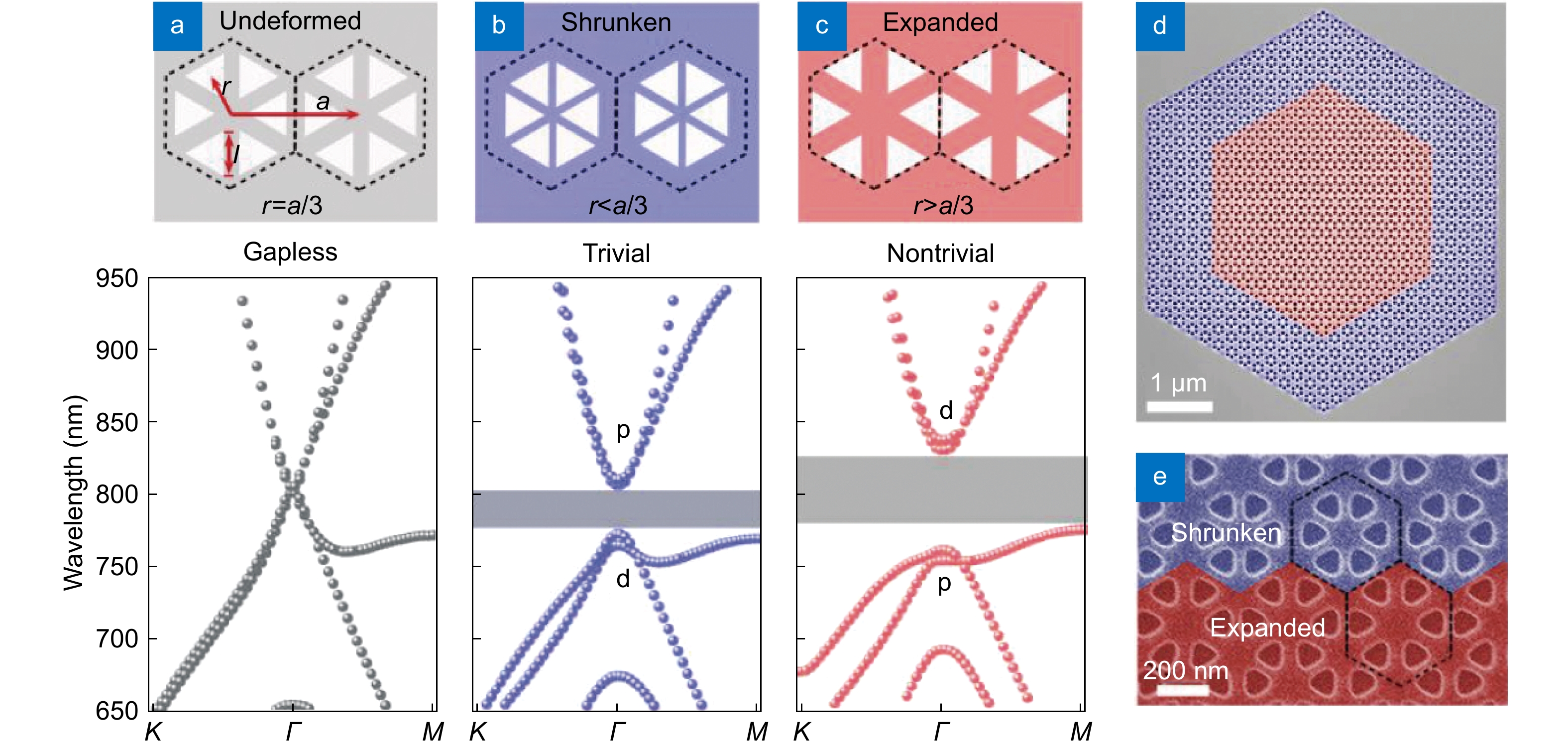
Figure 1.
The design and band structure of the proposed Z2 PTI. (a–c) Schematic of undeformed, shrunken, and expanded PhCs with their calculated band structures. The dashed hexagon outlines the structure unit cell, and the white triangle represents the hole area. The lattice constant a = 444 nm, the length of triangular hole l = 154 nm. The distance r between the unit cell center and triangular hole centroid for shrunken PhC is 138 nm, and for expanded PhC is 160 nm. The graphene-like band structure is formed when r = a/3 (undeformed), and topological trivial and non-trivial bandgaps can be opened at Γ point, when r < a/3 (shrunken) and r > a/3 (expanded), respectively. (d) Pseudo-colored SEM image of a fabricated structure. The outside shrunken and inside expanded PhCs are identified by blue and red regions, respectively. (e) Zoom-in SEM image of the interface area. Black dashed lines identify the unit cell of shrunken and expanded PhCs.
-
Figure 2.
Characterization of the Z2 topological edge state and its dark line. (a) Optical image of the fabricated Z2 PTI with a WSe2 monolayer transferred on the top. The interface between shrunken and expanded PhC regions, and the area of WSe2 monolayer fringe are marked with white and gray dashed lines, respectively. (b) PL spectra collected from the WSe2 monolayer upon the shrunken PhC (blue), expanded PhC (red), and near interface (green). The yellow shadow indicates the overlapped bandgap of shrunken and expanded PhCs. (c–e) PL mappings of bulk (expanded)-edge-bulk (shrunken) state at the resonance wavelength of 778 nm, 788 nm, and 802 nm. The defect triangle region of the WSe2 monolayer arises from the transferring process, like a wrinkle of the WSe2 monolayer, resulting in a bright triangle region in Fig. 2(c–e).
-
Figure 3.
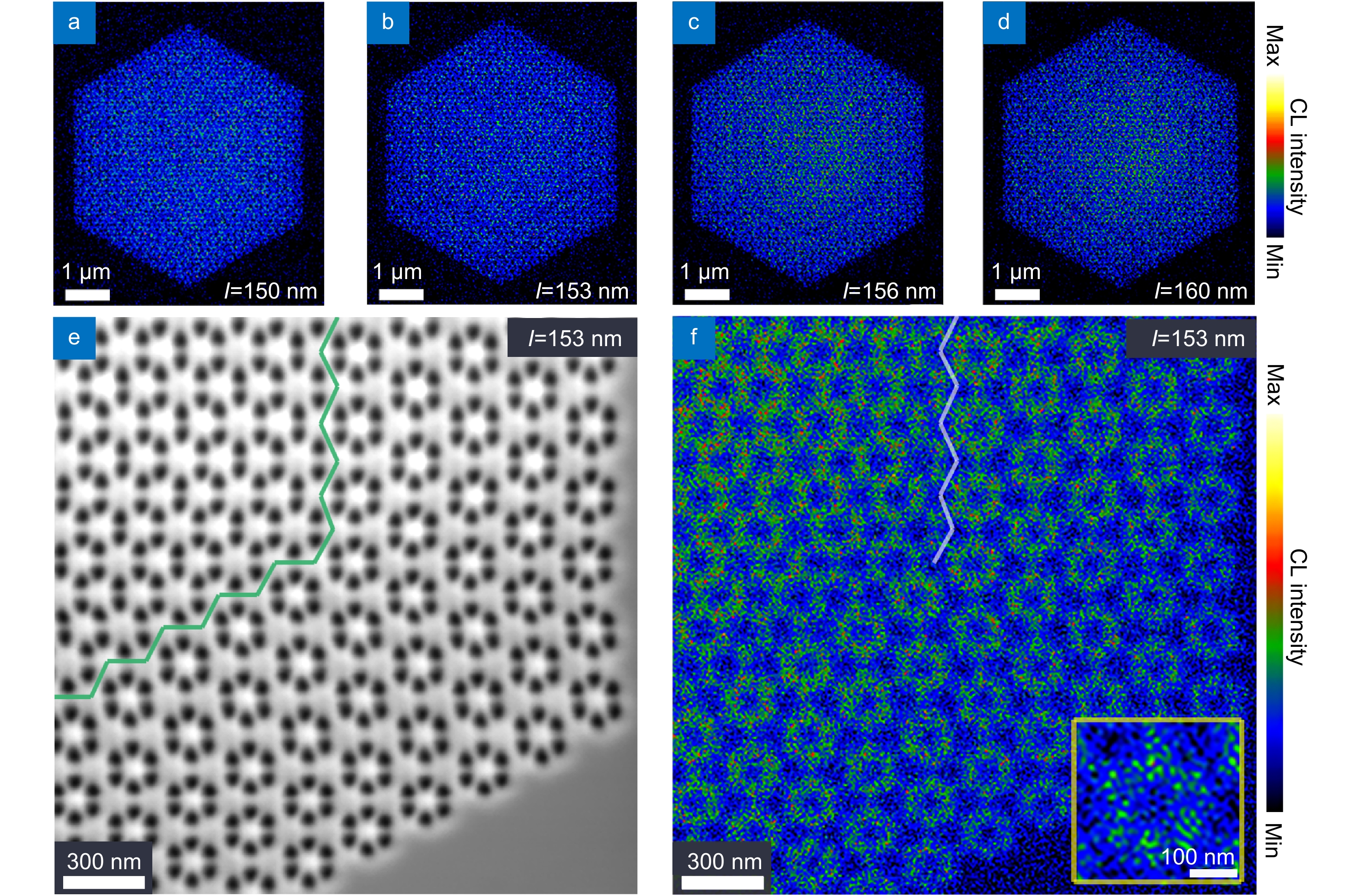
Deep-subwavelength LDOS imaging of the dark line of edge state. (a-d) CL mapping of four samples with increasing l to show the change of structure radiative LDOS. (e) Corner SEM image of the same sample in (b), the interface of two PhCs is marked with a solid green line. (f) Corresponding CL mapping of (e). The right part of the interface of two PhCs is marked with a solid white line. The inset is a detailed CL image of a single unit cell.
-
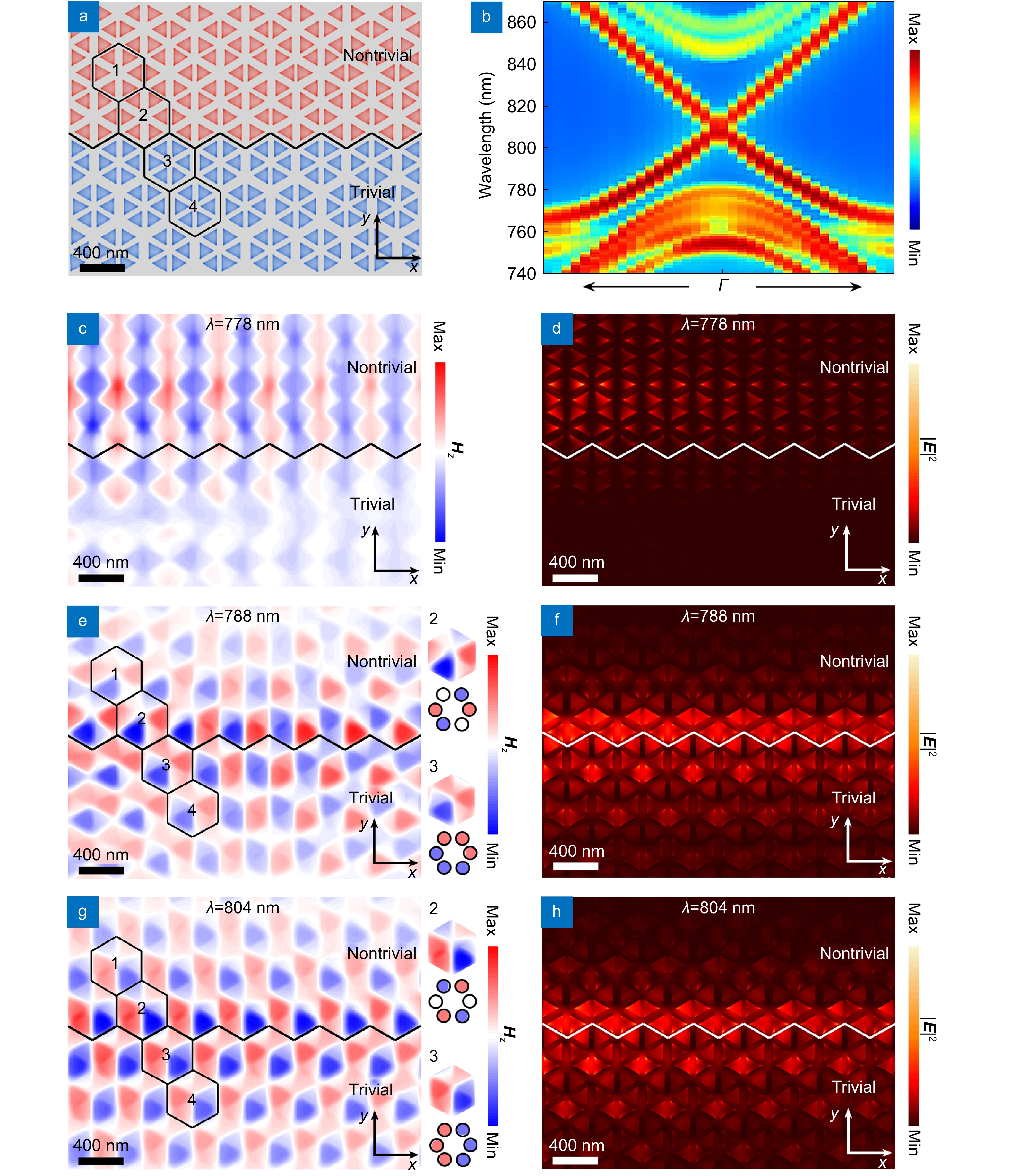
Figure 4.
Simulation of edge states. (a) Schematic of the interface that consists of expanded and shrunken PhCs. The interface of shrunken and expanded PhCs is marked as a zig-zag line. (b) Calculated band structure of the interface area. (c–d) Simulated expanded bulk state magnetic field (Hz) and electric intensity (|E|2) distributions at 778 nm (z = 0). (e–h) Simulated Z2 topological edge state magnetic field (Hz) and electric intensity (|E|2) distributions at 788 nm and 804 nm (z = 0). The upper (bottom) right-side of (e) and (g) shows an enlarged magnetic field of the unit cell 2 (3) and a general quadrupolar (dipolar) mode respectively. Parameters used in Fig. 4 are the same as parameters used in Fig. 1.


