
 E-mail Alert
 RSS
RSS
| Citation: |
Chen Z X, Yang Q X, Liu H L. Phase transition properties of the LIPSS induced by femtosecond laser direct writing on PMN-PT crystal[J]. Opto-Electron Eng, 2023, 50(3): 220275. doi: 10.12086/oee.2023.220275

|
Phase transition properties of the LIPSS induced by femtosecond laser direct writing on PMN-PT crystal
-
Abstract
In this paper, we propose a femtosecond laser-induced surface periodic structure (LIPSS) based on relaxed ferroelectric PMN-PT crystals. By changing the applied laser parameters, the period of the LIPSS structure is varied from 750 nm to 3 μm. Finally, the phase transition properties of the LIPSS structure are investigated by increasing the temperature. Compared to the phase transition properties of the substrate, the Curie temperature of the LIPSS structure is significantly reduced, and this will provide a possible new idea for the preparation of temperature-controlled modulators based on PMN-PT crystals.-
Keywords:
- femtosecond laser direct writing /
- LIPSS /
- PMN-PT crystal /
- phase transition
-

-
References
[1] Jia Y C, Wang S X, Chen F. Femtosecond laser direct writing of flexibly configured waveguide geometries in optical crystals: fabrication and application[J]. Opto-Electron Adv, 2020, 3(10): 190042. doi: 10.29026/oea.2020.190042 [2] Li L Q, Kong W J, Chen F. Femtosecond laser-inscribed optical waveguides in dielectric crystals: a concise review and recent advances[J]. Adv Photonics, 2022, 4(2): 024002. doi: 10.1117/1.AP.4.2.024002 [3] Li L Q, Li Z Q, Nie W J, et al. Femtosecond-laser-written S-curved waveguide in Nd: YAP crystal: fabrication and multi-gigahertz lasing[J]. J Light Technol, 2020, 38(24): 6845−6852. doi: 10.1109/JLT.2020.3015690 [4] Tan D Z, Sun X Y, Li Z L, et al. Effectively writing low propagation and bend loss waveguides in the silica glass by using a femtosecond laser[J]. Opt Lett, 2022, 47(18): 4766−4769. doi: 10.1364/OL.470670 [5] Yang Q X, Liu H L, He S, et al. Circular cladding waveguides in Pr: YAG fabricated by femtosecond laser inscription: Raman, luminescence properties and guiding performance[J]. Opto-Electron Adv, 2021, 4(2): 200005. doi: 10.29026/oea.2021.200005 [6] Xu X Y, Wang T X, Chen P C, et al. Femtosecond laser writing of lithium niobate ferroelectric nanodomains[J]. Nature, 2022, 609(7927): 496−501. doi: 10.1038/s41586-022-05042-z [7] Wu P F, Jiang X R, Zhang B, et al. Mode-controllable waveguide fabricated by laser-induced phase transition in KTN[J]. Opt Express, 2020, 28(17): 25633−25641. doi: 10.1364/OE.401407 [8] Zhang Q, Li M, Xu J, et al. Reconfigurable directional coupler in lithium niobate crystal fabricated by three-dimensional femtosecond laser focal field engineering[J]. Photonics Res, 2019, 7(5): 503−507. doi: 10.1364/PRJ.7.000503 [9] Lv H Y, Chu L R, Wang S X, et al. Layer-dependent nonlinear optical properties of two-dimensional InSe and its applications in waveguide lasers[J]. Opt Express, 2022, 30(13): 23986−23999. doi: 10.1364/OE.462811 [10] Xin C, Yang L, Li J W, et al. Conical hollow microhelices with superior swimming capabilities for targeted cargo delivery[J]. Adv Mater, 2019, 31(25): 1808226. doi: 10.1002/adma.201808226 [11] Chen W L, Yan Z, Tian J, et al. Flexible four-dimensional optical data storage enabled by single-pulse femtosecond laser irradiation in thermoplastic polyurethane[J]. Opt Lett, 2021, 46(13): 3211−3214. doi: 10.1364/OL.432092 [12] Lei Y H, Sakakura M, Wang L, et al. High speed ultrafast laser anisotropic nanostructuring by energy deposition control via near-field enhancement[J]. Optica, 2021, 8(11): 1365−1371. doi: 10.1364/OPTICA.433765 [13] Birnbaum M. Semiconductor surface damage produced by ruby lasers[J]. J Appl Phys, 1965, 36(11): 3688−3689. doi: 10.1063/1.1703071 [14] Li Y N, Wu Q, Yang M, et al. Uniform deep-subwavelength ripples produced on temperature controlled LiNbO3: Fe crystal surface via femtosecond laser ablation[J]. Appl Surf Sci, 2019, 478: 779−783. doi: 10.1016/j.apsusc.2019.02.037. [15] Zhang D S, Li X Z, Fu Y, et al. Liquid vortexes and flows induced by femtosecond laser ablation in liquid governing formation of circular and crisscross LIPSS[J]. Opto-Electron Adv, 2022, 5(2): 210066. doi: 10.29026/oea.2022.210066 [16] Zhang Y C, Jiang Q L, Long M Q, et al. Femtosecond laser-induced periodic structures: mechanisms, techniques, and applications[J]. Opto-Electron Sci, 2022, 1(6): 220005. doi: 10.29026/oes.2022.220005 [17] Ren Y Y, Zhang L M, Romero C, et al. Femtosecond laser irradiation on Nd: YAG crystal: surface ablation and high-spatial-frequency nanograting[J]. Appl Surf Sci, 2018, 441: 372−380. doi: 10.1016/j.apsusc.2018.01.217 [18] Huang J, Jiang L, Li X W, et al. Fabrication of highly homogeneous and controllable nanogratings on silicon via chemical etching-assisted femtosecond laser modification[J]. Nanophotonics, 2019, 8(5): 869−878. doi: 10.1515/nanoph-2019-0056 [19] Cho D H, Hong S H, Lee W J, et al. Colorful solar cells utilizing off-axis light diffraction via transparent nanograting structures[J]. Nano Energy, 2021, 80: 105550. doi: 10.1016/j.nanoen.2020.105550 [20] Fang Z, Jiang X D, Tian X, et al. Ultratransparent PMN-PT electro-optic ceramics and its application in optical communication[J]. Adv Opt Mater, 2021, 9(13): 2002139. doi: 10.1002/adom.202002139 [21] Deng C G, Ye L X, He C J, et al. Reporting excellent transverse piezoelectric and electro-optic effects in transparent rhombohedral PMN-PT single crystal by engineered domains[J]. Adv Mater, 2021, 33(43): 2103013. doi: 10.1002/adma.202103013 [22] Li Q, Liu Y B, Liu J F, et al. Enhanced piezoelectric properties and improved property uniformity in Nd-doped PMN-PT relaxor ferroelectric single crystals[J]. Adv Funct Mater, 2022, 32(25): 2201719. doi: 10.1002/adfm.202201719 [23] Piredda G, Stroj S, Ziss D, et al. Micro-machining of PMN-PT crystals with ultrashort laser pulses[J]. Appl Phys A, 2019, 125(3): 201. doi: 10.1007/s00339-019-2460-9 [24] Chen X, Liu D W, Liu S, et al. Optical induction and erasure of ferroelectric domains in tetragonal PMN-38PT crystals[J]. Adv Opt Mater, 2022, 10(4): 2102115. doi: 10.1002/adom.202102115 [25] Shen T L, Si J H, Chen T, et al. Fabrication of microgrooves in PMN-PT using femtosecond laser irradiation and acid etching[J]. Appl Opt, 2022, 61(21): 6234−6240. doi: 10.1364/AO.459556 [26] Sipe J E, Young J F, Preston J S, et al. Laser-induced periodic surface structure. I. Theory[J]. Phys Rev B, 1983, 27(2): 1141−1154. doi: 10.1103/PhysRevB.27.1141 -
Overview
With the development of modern manufacturing, the size of optical devices is gradually developing towards miniaturization, and integrated optics is also developing to become a topical area of research for many scholars. One of the methods used for producing micro/nano optical devices is femtosecond laser direct writing, a fine three-dimensional processing technique that has been extensively studied by many scholars for its applicability to most materials and can be applied to the fabrication of a wide range of optical devices. Micro/nano-optical devices prepared by femtosecond laser direct writing in crystals have been applied in a broad range of applications in different wavelengths. PMN-PT crystal with relaxed ferroelectric has attracted much attention in recent years for its superior piezoelectric property and large electromechanical coupling coefficient, and its application in the infrared band is more prominent, so the fabrication of the optical devices based on PMN-PT crystal has gradually become a relevant research hotspot. The LIPSS is one of the micro/nano-structures that can be processed by femtosecond laser direct writing. The LIPSS is prevalent in many materials and has been found in metals, semiconductors, dielectrics, etc. Similarly, LIPSS can be induced by femtosecond lasers in PMN-PT crystal. The LIPSS has a wide range of applications in the fields of anti-reflectivity, permanent coloration, and wettability. Nevertheless, the physical processes and the mechanisms involved in the formation of LIPSS have different interpretations in different materials. In this paper, we describe the LIPSS induced by femtosecond laser on the surface of the PMN-PT crystal and characterize it theoretically. We have achieved a change in the period of the LIPSS from 750 nm to 3000 nm after experimenting with different laser parameters. Afterward, we simultaneously obtained the phase transition of the LIPSS in PMN-PT crystal through temperature modulation, and this phase transition can be analyzed by the variation of the Raman spectra. At the same time, we have obtained the Curie temperature for the LIPSS structure that is approximately 10 ℃ lower than that of the PMN-PT crystal and have analyzed the phase transition process through the structural properties of the PMN-PT crystal. The results of our experiments and analyzes on the LIPSS in PMN-PT crystal reported in this paper can provide some experience for the subsequent development of the optical devices related to the LIPSS in PMN-PT crystal.
-
Access History

Export File
Citation
Chen Z X, Yang Q X, Liu H L. Phase transition properties of the LIPSS induced by femtosecond laser direct writing on PMN-PT crystal[J]. Opto-Electron Eng, 2023, 50(3): 220275. doi: 10.12086/oee.2023.220275
Format
Content
 DownLoad:
-
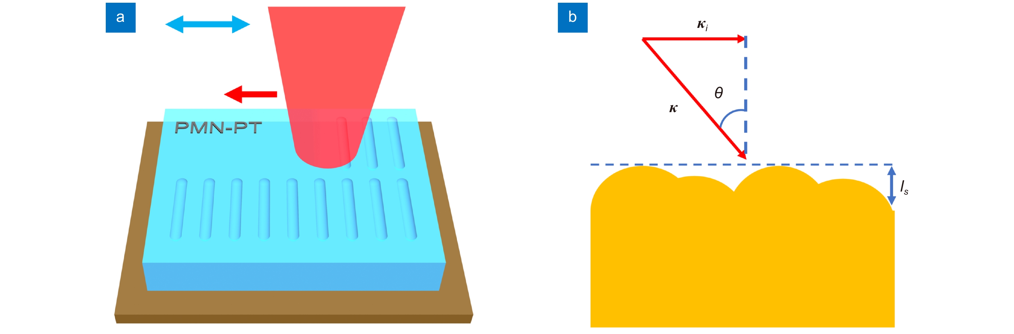
Figure 1.
Schematic diagram of femtosecond laser processing. (a) Schematic diagram of LIPSS in the PMN-PT crystal by femtosecond laser direct writing, the red arrow represents the direction of laser scanning, the blue arrow represents the direction of polarization of the laser; (b) Schematic diagram of the femtosecond laser-induced LIPSS
-
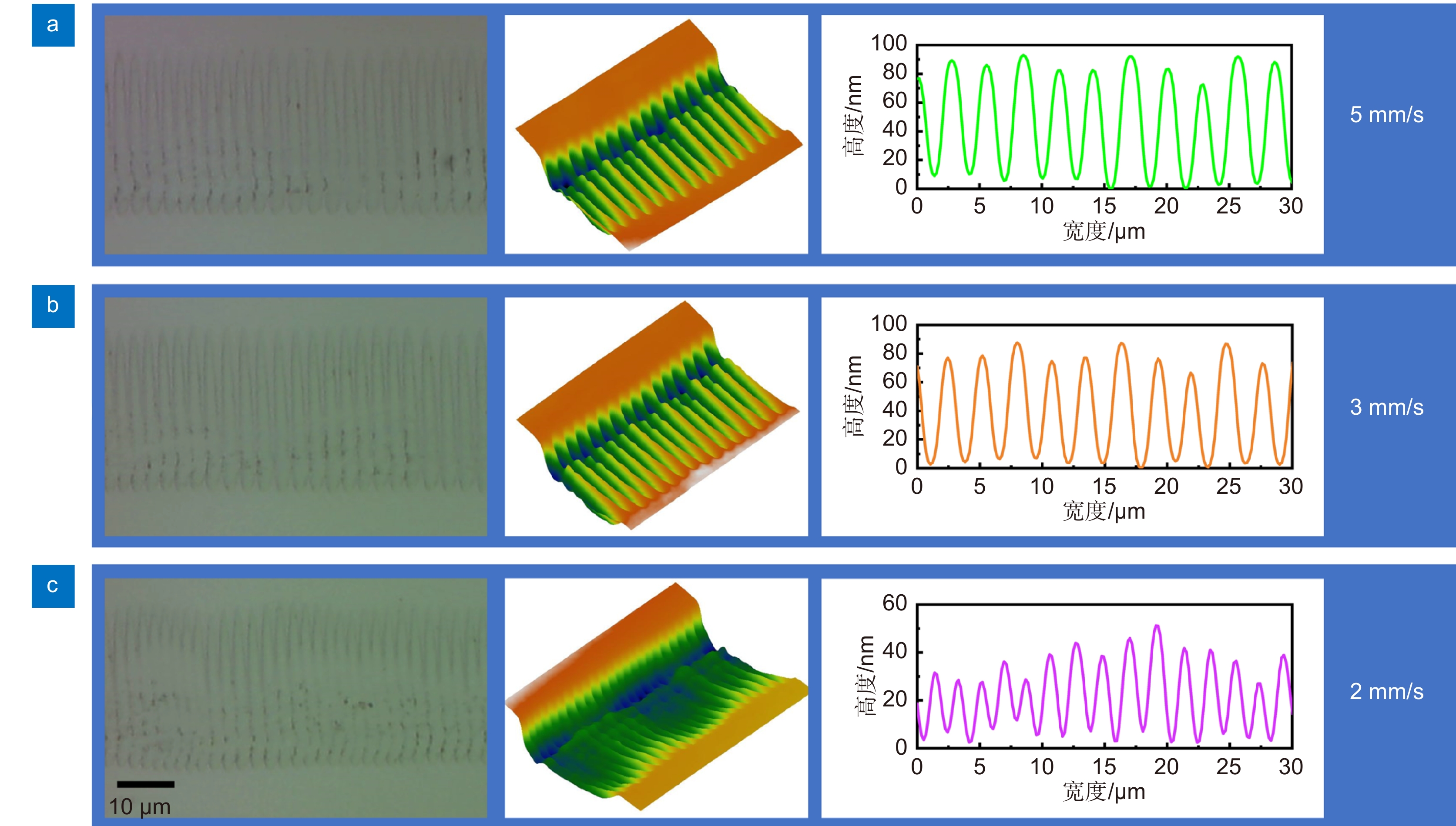
Figure 2.
Morphology of SWPSS induced by femtosecond laser. (a)~(c) SWPSS at velocities of 5 mm/s, 3 mm/s, and 2 mm/s respectively
-
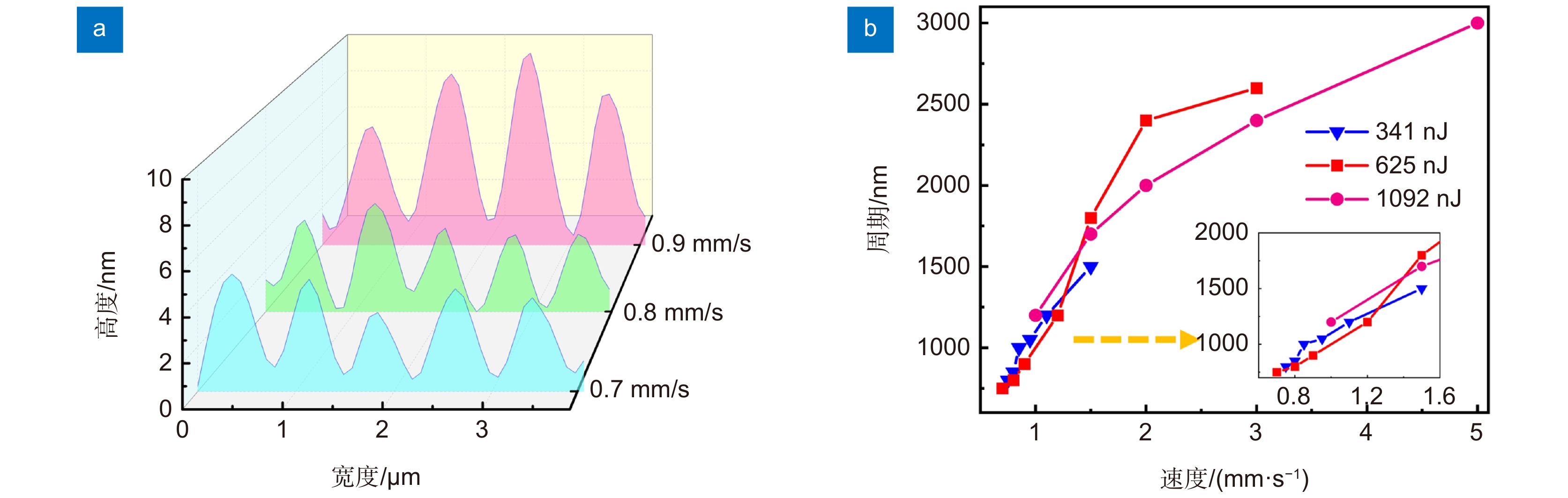
Figure 3.
(a) Morphology of the LSFL with velocities of 0.7 mm/s, 0.8 mm/s, and 0.9 mm/s respectively; (b) Period of LIPSS in relation to laser parameters
-
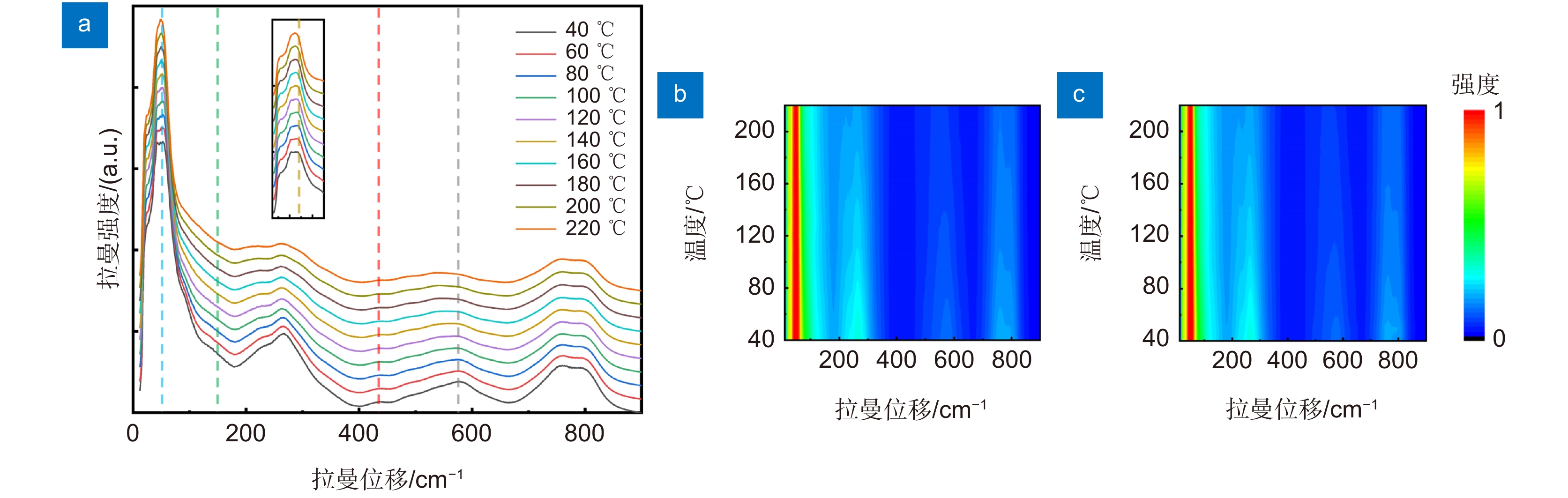
Figure 4.
(a) Raman spectra of the LIPSS with the variation of temperature, the inset shows the variation of the Raman spectra at the Raman shift near the 50 cm−1 ; (b) Intensity of Raman signal of the PMN-PT crystal with the variation of temperature; (c) Intensity of Raman signal of the LIPSS with the variation of temperature
- Figure .


