
 E-mail Alert
 RSS
RSS
-
摘要:
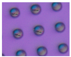
采用光刻胶热熔法制作具有特定尺寸的微透镜,制作的微透镜能将微透镜阵列技术应用于短波1 μm ~3 μm红外探测器中,有效地提高探测器件的光电性能。采用AZ P4620厚光刻胶,利用紫外光刻技术,对透镜制作中的前烘、曝光和显影、坚膜、热熔等工艺进行了深入细致的实验研究,确定了最优的工艺参数,实现了球冠直径在(5.5±0.5) μm,曲率半径3 μm的微透镜,且透镜有很好的均匀性和一致性,满足近红外探测器件的要求。
 Abstract:
A microlens with a specific size is fabricated by using melting photoresist, and the microlens can be applied to a shortwave 1 μm ~3 μm infrared detector, which can effectively improve the photoelectric performance of the detector. Using AZP4620 thick photoresist and UV lithography technology, the lens production in the soft bake, exposure and development, hardening, hot melt and other processes were carried out in-depth and detailed experimental study was done to determine the optimal process parameters. The micro-lens with a crown diameter of (5.5 ± 0.5) μm and a radius of curvature of 3 μm was realized. The lens has good uniformity and consistency to meet the requirements of near infrared detection device.
-
Key words:
- microlens array /
- melting photoresist /
- pre-baking /
- hot melt
-

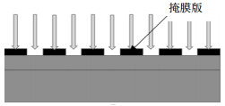
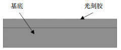
Abstract: Most of our domestic infrared detector’s photosensitive surface is less than the pixel surface area. A part ofthe incident light irradiates to the photosensitive area between the dead zone, and this part is not used but reflectedand scattered. The microlens array with specific size was fabricated by photoresist fusion method, then a microlensarray was used to converge to a 1 μm ~3 μm infrared detector, the surface area of the infrared detector can be expanded to reduce noise of the infrared detector and prevent incident light from entering the dead zone. The mainprocess steps include: substrate cleaning, coating and glue, soft baking, exposure and development, baking, hot melt,ion beam etching and so on. The specific process steps: first, in order to obtain the photoresist pattern required for themicromirror curvature, we chose the AZP4620 positive photoresist for the thick film, and the refractive index of thephotoresist was 1.64. Second, the substrate treatment, removing the substrate surface grease and other impurities toensure that the substrate and the photoresist had good adhesion. Third, the substrate was coated with a uniform photoresist, and the photoresist was placed under the mask plate which had been set in advance and subjected to UV exposure, the corresponding cylindrical colloid was formed by the development of the image; Fourth, the substrate putinto the rapid annealing furnace for hot-melt, the photoresist was heated in the rapid annealing furnace, the surfacearea of the melted photoresist would shrink to a minimum and the surface energy was the lowest due to the combinedaction of the surface tension and the substrate adhesion. After the hot melt getting a stable spherical crown microlensmust require photoresist cylinder that reduced the amount of gravity is equal to the increase in the amount of potential energy. In the experiment, not any size and the thickness of the cylindrical colloid can form good spherical surfaceshape after hot melt to meet the design requirements of spherical shape by the photoresist cylinder diameter size,height, and the infiltration degree of glue and basal decision. Photoresist as an amorphous polymer is composed of avariety of chemical composition. The melting point of the photoresist is not an accurate temperature, but a temperature range in which the state of the photoresist exhibits a liquid state. Because of the different types of photoresist, themelting point range is different. Finally, the uniform microlens array was obtained with an ion beam etch machine. Byoptimizing the temperature and time parameters of each step process, the microlens with a crown diameter of (5.5 ±0.5) μm and a radius of curvature of 3 μm was realized, the microlens had good uniformity and consistency, and theinfrared detection was carried out in the 1 μm ~3 μm band device requirements.
-

-

图 5 前烘温度和时间. (a)前烘温度60 ℃,时间45 min. (b)前烘温度85 ℃,时间20 min. (c)前烘100 ℃,时间8 min.
Figure 5. Pre-baking temperature and time. (a) Pre-baking temperature 60℃, time 45 min. (b) Pre-bakingtemperature 85℃, time 20 min.(c) Pre-baking temperature 100℃, time 8 min.
表 1 甩胶机设置参数.
Table 1. The parameter set by glue machine.
除湿剂旋转参数P17/Hz 旋转除湿剂所需时间的参数P81/s 涂光刻胶所需时间的参数P82/s 旋转光刻胶的参数P19/Hz 旋转光刻胶所需时间的参数P83/s 34 15 15 102 30  下载: 导出CSV
表 2 前烘温度100 ℃, 曝光25 s, 显影8~9 s
Table 2. Pre-baking temperature 100 ℃, exposure 25 s and development 8~9 s
前烘时间/min 6 7 8 9 10 11 15 20 25 胶的厚度/pm 3.34 3.56 3.13 3.07 2.98 2.97 2.89 2.85 2.86
下载: 导出CSV
表 3 前烘温度100 ℃, 曝光20 s, 显影8~9 s
Table 3. Pre-baking temperature 100 ℃, exposure 20 s and development 8~9 s
前烘时间/min 6 7 8 9 10 7 8 9 10 11 15 20 25 胶的厚度/pm 3.12 3.14 3.25 3.47 3.21 2.77 2.63 2.59 2.53
下载: 导出CSV
表 4 微透镜阵列热熔条件实验.
Table 4. Experimental study on melting conditions of microlens array.
热熔温度/℃ 热熔时间/s 热熔前上台面/pm 热熔前下台面/pm 热熔前高度/pm 球冠高度h/pm 球冠直径D/pm 热熔前体积V1/pm3 球冠体积V2/pm3 V2/V1/% 球冠曲率半径R = (4h2+D2)/8h 140 180 3.05 5.98 1.89 1.7 5.3 31.37 21.36 68.08 2.92 140 240 3.05 5.98 1.89 1.68 5.4 31.37 21.71 69.21 3.01 140 300 3.05 5.98 1.89 1.65 5.45 31.37 21.54 68.67 3.07 150 180 3.05 5.98 1.89 1.58 5.32 31.37 19.62 62.55 3.03 150 240 3.05 5.98 1.89 1.56 5.42 31.37 19.94 63.56 3.13 150 300 3.05 5.98 1.89 1.53 5.48 31.37 19.92 63.50 3.21 160 180 3.05 5.98 1.89 1.5 5.57 31.37 20.06 63.96 3.34 160 240 3.05 5.98 1.89 1.48 5.68 31.37 20.4 65.04 3.46 160 300 3.05 5.98 1.89 1.46 5.87 31.37 21.37 68.13 3.68
下载: 导出CSV
-
[1] 王峥一, 武伟璐, 牛邦玉.微透镜及其阵列研究概况[J].科技与创新, 2016(11):102-103. http://www.wanfangdata.com.cn/details/detail.do?_type=perio&id=wjsjxx201611079
[2] Oikawa M, Iga K, Sanada T, et al. Array of distributed-index planar micro-lenses prepared from ion exchange technique[J]. JapaneseJournal of Applied Physics, 1981, 20(4):L296-L298. http://cn.bing.com/academic/profile?id=70c5cebd8e0c3b0ad6bb422bb06f1997&encoded=0&v=paper_preview&mkt=zh-cn
[3] Totsu K, Fujishiro K, Tanaka S, et al. Fabrication of three-dimensional microstructure using maskless gray-scale lithography[J]. Sensors and Actuators A:Physical, 2006, 130-131:387-392. https://www.sciencedirect.com/science/article/pii/S092442470500717X
[4] Shiang J J, Faircloth T J, Duggal A R. Experimental demonstration of increased organic light emitting device output via volumetric light scattering[J]. Journal of Applied Physics, 2004, 95(5):2889-2895. doi: 10.1063/1.1644038
[5] Kim C S, Ahn S H, Jang D Y. Review:developments in micro/nanoscale fabrication by focused ion beams[J]. Vacuum, 2012, 86(8):1014-1035. doi: 10.1016/j.vacuum.2011.11.004
[6] 杨西, 杨玉华.化学气相沉积技术的研究与应用进展[J].甘肃水利水电技术, 2008, 44(3):211-213. http://industry.wanfangdata.com.cn/dl/Detail/Periodical?id=Periodical_gsslsdjs200803024
[7] 孙丰强, 蔡伟平, 李越, 等.基于二维胶体晶体刻蚀法的纳米颗粒阵列[J].物理, 2003, 32(4):223-227. http://edu.wanfangdata.com.cn/Periodical/Detail/wl200304003
Sun Fengqiang, Cai Weiping, Li Yue, et al. Nanoparticle array synthesized by two-dimensional colloid crystal lithography[J]. Physics, 2003, 32(4):223-227. http://edu.wanfangdata.com.cn/Periodical/Detail/wl200304003
[8] Hanarp P. Optical properties of nanometer disks, holes and rings prepared by colloidal lithography[D]. Göteborg: Chalmers University of Technology, 2003: 1-56.
[9] 甘代伟.微透镜阵列制作技术研究[J].装备制造技术, 2011(9):44-45, 49. http://cdmd.cnki.com.cn/Article/CDMD-10007-1016717695.htm
Gan Daiwei. Fabrication technology research of microlens array[J]. Equipment Manufacturing Technology, 2011(9):44-45, 49. http://cdmd.cnki.com.cn/Article/CDMD-10007-1016717695.htm
[10] Ni Z H, Wang H M, Kasim J, et al. Graphene thickness determination using reflection and contrast spectroscopy[J].Nano Letters, 2007, 7(9):2758-2763. doi: 10.1021/nl071254m
[11] Lim C S, Hong M H, Lin Y, et al. Microlens array fabrication by laser interference lithography for super-resolution surface nanopatterning[J]. Applied Physics Letters, 2006, 89(19):191125. doi: 10.1063/1.2374809
[12] 唐雄贵, 姚欣, 郭永康, 等.烘焙工艺条件对厚胶光刻面形的影响[J].微细加工技术, 2005(3):31-35. https://www.wenkuxiazai.com/doc/b6b89f4d2e3f5727a5e9628a-4.html
Tang Xionggui, Yao Xin, Guo Yongkang, et al. Effect of baking process conditions on surface profile of lithography for thick film resists[J]. Microfabrication Technology, 2005(3):31-35. https://www.wenkuxiazai.com/doc/b6b89f4d2e3f5727a5e9628a-4.html
[13] 刘德森.微小光学与微透镜阵列[M].北京:科学出版社, 2013:210-214.
-


 点击扫一扫
点击扫一扫
图(6)
表(4)
计量
- 文章访问数: 6177
- PDF下载数: 3729
- 施引文献: 0


