| Citation: | Jiang QL, Chen L, Liu JK, Zhang YC, Zhang SA et al. Periodic transparent nanowires in ITO film fabricated via femtosecond laser direct writing. Opto-Electron Sci 2, 220002 (2023). doi: 10.29026/oes.2023.220002 |
Periodic transparent nanowires in ITO film fabricated via femtosecond laser direct writing
-
Abstract
This paper reports the fabrication of regular large-area laser-induced periodic surface structures (LIPSSs) in indium tin oxide (ITO) films via femtosecond laser direct writing focused by a cylindrical lens. The regular LIPSSs exhibited good properties as nanowires, with a resistivity almost equal to that of the initial ITO film. By changing the laser fluence, the nanowire resistances could be tuned from 15 to 73 kΩ/mm with a consistency of ±10%. Furthermore, the average transmittance of the ITO films with regular LIPSSs in the range of 1200–2000 nm was improved from 21% to 60%. The regular LIPSS is promising for transparent electrodes of nano-optoelectronic devices—particularly in the near-infrared band. -

-
References
[1] Liu HY, Avrutin V, Izyumskaya N, Özgür Ü, Morkoç H. Transparent conducting oxides for electrode applications in light emitting and absorbing devices. Superlattice Microst 48, 458–484 (2010). doi: 10.1016/j.spmi.2010.08.011 [2] Exarhos GJ, Zhou XD. Discovery-based design of transparent conducting oxide films. Thin Solid Films 515, 7025–7052 (2007). doi: 10.1016/j.tsf.2007.03.014 [3] Ma ZZ, Li ZR, Liu K, Ye CR, Sorger VJ. Indium-tin-oxide for high-performance electro-optic modulation. Nanophotonics 4, 198–213 (2015). doi: 10.1515/nanoph-2015-0006 [4] Kim H, Gilmore CM, Piqué A, Horwitz JS, Mattoussi H et al. Electrical, optical, and structural properties of indium–tin–oxide thin films for organic light-emitting devices. J Appl Phys 86, 6451–6461 (1999). doi: 10.1063/1.371708 [5] Tahar RBH, Ban T, Ohya Y, Takahashi Y. Tin doped indium oxide thin films: electrical properties. J Appl Phys 83, 2631–2645 (1998). doi: 10.1063/1.367025 [6] Parra-Barranco J, García-García FJ, Rico V, Borrás A, López-Santos C et al. Anisotropic in-plane conductivity and dichroic gold plasmon resonance in plasma-assisted ITO thin films e-beam-evaporated at oblique angles. ACS Appl Mater Interfaces 7, 10993–11001 (2015). doi: 10.1021/acsami.5b02197 [7] Bonse J, Höhm S, Kirner SV, Rosenfeld A, Krüger J. Laser-induced periodic surface structures — a scientific evergreen. IEEE J Sel Top Quant Electron 23, 9000615 (2017). [8] Shimotsuma Y, Kazansky PG, Qiu JR, Hirao K. Self-organized nanogratings in glass irradiated by ultrashort light pulses. Phys Rev Lett 91, 247405 (2003). doi: 10.1103/PhysRevLett.91.247405 [9] Jia TQ, Chen H, Zhang YM. Photon absorption of conduction-band electrons and their effects on laser-induced damage to optical materials. Phys Rev B 61, 16522–16529 (2000). doi: 10.1103/PhysRevB.61.16522 [10] Zhang B, Tan DZ, Wang Z, Liu XF, Xu BB et al. Self-organized phase-transition lithography for all-inorganic photonic textures. Light Sci Appl 10, 93 (2021). doi: 10.1038/s41377-021-00534-5 [11] Lin ZY, Liu HG, Ji LF, Lin WX, Hong MH. Realization of ~10 nm features on semiconductor surfaces via femtosecond laser direct patterning in far field and in ambient air. Nano Lett 20, 4947–4952 (2020). doi: 10.1021/acs.nanolett.0c01013 [12] Zhang DS, Sugioka K. Hierarchical microstructures with high spatial frequency laser induced periodic surface structures possessing different orientations created by femtosecond laser ablation of silicon in liquids. Opto-Electron Adv 2, 190002 (2019). [13] Zhang DS, Wu LC, Ueki M, Ito Y, Sugioka K. Femtosecond laser shockwave peening ablation in liquids for hierarchical micro/nanostructuring of brittle silicon and its biological application. Int J Extrem Manuf 2, 045001 (2020). doi: 10.1088/2631-7990/abb5f3 [14] Zhao B, Zheng X, Lei YH, Xie HB, Zou TT et al. High-efficiency-and-quality nanostructuring of molybdenum surfaces by orthogonally polarized blue femtosecond lasers. Appl Surf Sci 572, 151371 (2022). doi: 10.1016/j.apsusc.2021.151371 [15] Chen L, Cao KQ, Li YL, Liu JK, Zhang SA et al. Large-area straight, regular periodic surface structures produced on fused silica by the interference of two femtosecond laser beams through cylindrical lens. Opto-Electron Adv 4, 200036 (2021). doi: 10.29026/oea.2021.200036 [16] Zhang YC, Jiang QL, Cao KQ, Chen TQ, Cheng K et al. Extremely regular periodic surface structures in a large area efficiently induced on silicon by temporally shaped femtosecond laser. Photonics Res 9, 839–847 (2021). doi: 10.1364/PRJ.418937 [17] Zhou R, Huang TT, Lu YY, Hong MH. Tunable coloring via post-thermal annealing of laser-processed metal surface. Appl Sci 8, 1716 (2018). doi: 10.3390/app8101716 [18] Liu HG, Lin WX, Hong MH. Surface coloring by laser irradiation of solid substrates. APL Photonics 4, 051101 (2019). doi: 10.1063/1.5089778 [19] Chen L, Cao KQ, Liu JK, Jia TQ, Li YL et al. Surface birefringence of regular periodic surface structures produced on glass coated with an indium tin oxide film using a low-fluence femtosecond laser through a cylindrical lens. Opt Express 28, 30094–30106 (2020). doi: 10.1364/OE.402037 [20] Zou TT, Zhao B, Xin W, Wang FY, Xie HB et al. Birefringent response of graphene oxide film structurized via femtosecond laser. Nano Res 15, 4490–4499 (2022). doi: 10.1007/s12274-021-3505-x [21] Cunha A, Serro AP, Oliveira V, Almeida A, Vilar R et al. Wetting behaviour of femtosecond laser textured Ti–6Al–4V surfaces. Appl Surf Sci 265, 688–696 (2013). doi: 10.1016/j.apsusc.2012.11.085 [22] Zhao YZ, Su YL, Hou XY, Hong MH. Directional sliding of water: biomimetic snake scale surfaces. Opto-Electron Adv 4, 210008 (2021). doi: 10.29026/oea.2021.210008 [23] Su YL, Zhao YZ, Jiang SY, Hou XY, Hong MH. Anisotropic superhydrophobic properties of bioinspired surfaces by laser ablation of metal substrate inside water. Adv Mater Interfaces 8, 2100555 (2021). doi: 10.1002/admi.202100555 [24] Reinhardt HM, Maier P, Kim HC, Rhinow D, Hampp N. Nanostructured transparent conductive electrodes for applications in harsh environments fabricated via nanosecond laser‐induced periodic surface structures (LIPSS) in indium–tin oxide films on glass. Adv Mater Interfaces 6, 1900401 (2019). [25] Pan AF, Wang WJ, Liu B, Mei XS, Yang HZ et al. Formation of high-spatial-frequency periodic surface structures on indium-tin-oxide films using picosecond laser pulses. Mater Des 121, 126–135 (2017). doi: 10.1016/j.matdes.2017.02.055 [26] Liu P, Wang WJ, Pan AF, Xiang Y, Wang DP. Periodic surface structures on the surface of indium tin oxide film obtained using picosecond laser. Opt Laser Technol 106, 259–264 (2018). doi: 10.1016/j.optlastec.2018.04.019 [27] Solodar A, Cerkauskaite A, Drevinskas R, Kazansky PG, Abdulhalim I. Ultrafast laser induced nanostructured ITO for liquid crystal alignment and higher transparency electrodes. Appl Phys Lett 113, 081603 (2018). doi: 10.1063/1.5040692 [28] Cerkauskaite A, Drevinskas R, Solodar A, Abdulhalim I, Kazansky PG. Form-birefringence in ITO thin films engineered by ultrafast laser nanostructuring. ACS Photonics 4, 2944–2951 (2017). doi: 10.1021/acsphotonics.7b01082 [29] Miccoli I, Edler F, Pfnür H, Tegenkamp C. The 100th anniversary of the four-point probe technique: the role of probe geometries in isotropic and anisotropic systems. J Phys Condens Matter 27, 223201 (2015). doi: 10.1088/0953-8984/27/22/223201 [30] Hong S, Lee H, Yeo J, Ko SH. Digital selective laser methods for nanomaterials: from synthesis to processing. Nano Today 11, 547–564 (2016). doi: 10.1016/j.nantod.2016.08.007 [31] Zhang FZ, Chen L, Zhang YC, Jiang QL, Feng DH et al. High-performance birefringence of periodic nanostructures in FTO thin film fabricated by IR-UV femtosecond laser. Front Phys 10, 861389 (2022). doi: 10.3389/fphy.2022.861389 [32] Cao KQ, Chen L, Wu HC, Liu JK, Cheng K et al. Large-area commercial-grating-quality subwavelength periodic ripples on silicon efficiently fabricated by gentle ablation with femtosecond laser interference via two cylindrical lenses. Opt Laser Technol 131, 106441 (2020). doi: 10.1016/j.optlastec.2020.106441 [33] Cheng K, Liu JK, Cao KQ, Chen L, Zhang YC et al. Ultrafast dynamics of single-pulse femtosecond laser-induced periodic ripples on the surface of a gold film. Phys Rev B 98, 184106 (2018). doi: 10.1103/PhysRevB.98.184106 [34] Zhou K, Jia X, Jia TQ, Cheng K, Cao KQ et al. The influences of surface plasmons and thermal effects on femtosecond laser-induced subwavelength periodic ripples on Au film by pump-probe imaging. J Appl Phys 121, 104301 (2017). doi: 10.1063/1.4978375 [35] Bian QM, Yu XM, Zhao BZ, Chang ZH, Lei ST. Femtosecond laser ablation of indium tin-oxide narrow grooves for thin film solar cells. Opt Laser Technol 45, 395–401 (2013). doi: 10.1016/j.optlastec.2012.06.018 [36] Fernandes SA, Schoeps B, Kowalick K, Nett R, Esen C et al. Femtosecond laser ablation of ITO/ZnO for thin film solar cells. Phys Procedia 41, 802–809 (2013). doi: 10.1016/j.phpro.2013.03.151 [37] Cheng CW, Lee IM, Chen JS. Femtosecond laser processing of indium-tin-oxide thin films. Opt Lasers Eng 69, 1–6 (2015). [38] Hertwig A, Martin S, Krüger J, Kautek W. Interaction area dependence of the ablation threshold of ion-doped glass. Thin Solid Films 453–454, 527–530 (2004). [39] Jia TQ, Baba M, Suzuki M, Ganeev RA, Kuroda H et al. Fabrication of two-dimensional periodic nanostructures by two-beam interference of femtosecond pulses. Opt Express 16, 1874–1878 (2008). doi: 10.1364/OE.16.001874 [40] Kim H, Piqué A, Horwitz JS, Mattoussi H, Murata H et al. Indium tin oxide thin films for organic light-emitting devices. App Phys Lett 74, 3444–3446 (1999). doi: 10.1063/1.124122 [41] Zhao J, Ding XH, Miao JH, Hu JF, Wan H et al. Improvement in light output of ultraviolet light-emitting diodes with patterned double-layer ITO by laser direct writing. Nanomaterials 9, 203 (2019). doi: 10.3390/nano9020203 [42] Shigesato Y, Hayashi Y, Haranoh T. Doping mechanisms of tin‐doped indium oxide films. Appl Phys Lett 61, 73–75 (1992). doi: 10.1063/1.107673 [43] Jia JJ, Takaya A, Yonezawa T, Yamasaki K, Nakazawa H et al. Carrier densities of Sn-doped In2O3 nanoparticles and their effect on X-ray photoelectron emission. J Appl Phys 125, 245303 (2019). doi: 10.1063/1.5096364 [44] Petukhov IA, Shatokhin AN, Putilin FN, Rumyantseva MN, Kozlovskii VF et al. Pulsed laser deposition of conductive indium tin oxide thin films. Inorg Mater 48, 1020–1025 (2012). doi: 10.1134/S0020168512100068 -
Supplementary Information
Supplementary information Periodic transparent nanowires in ITO film fabricated via femtosecond laser direct writing 
-
Access History

Article Metrics
-
Figure 1.
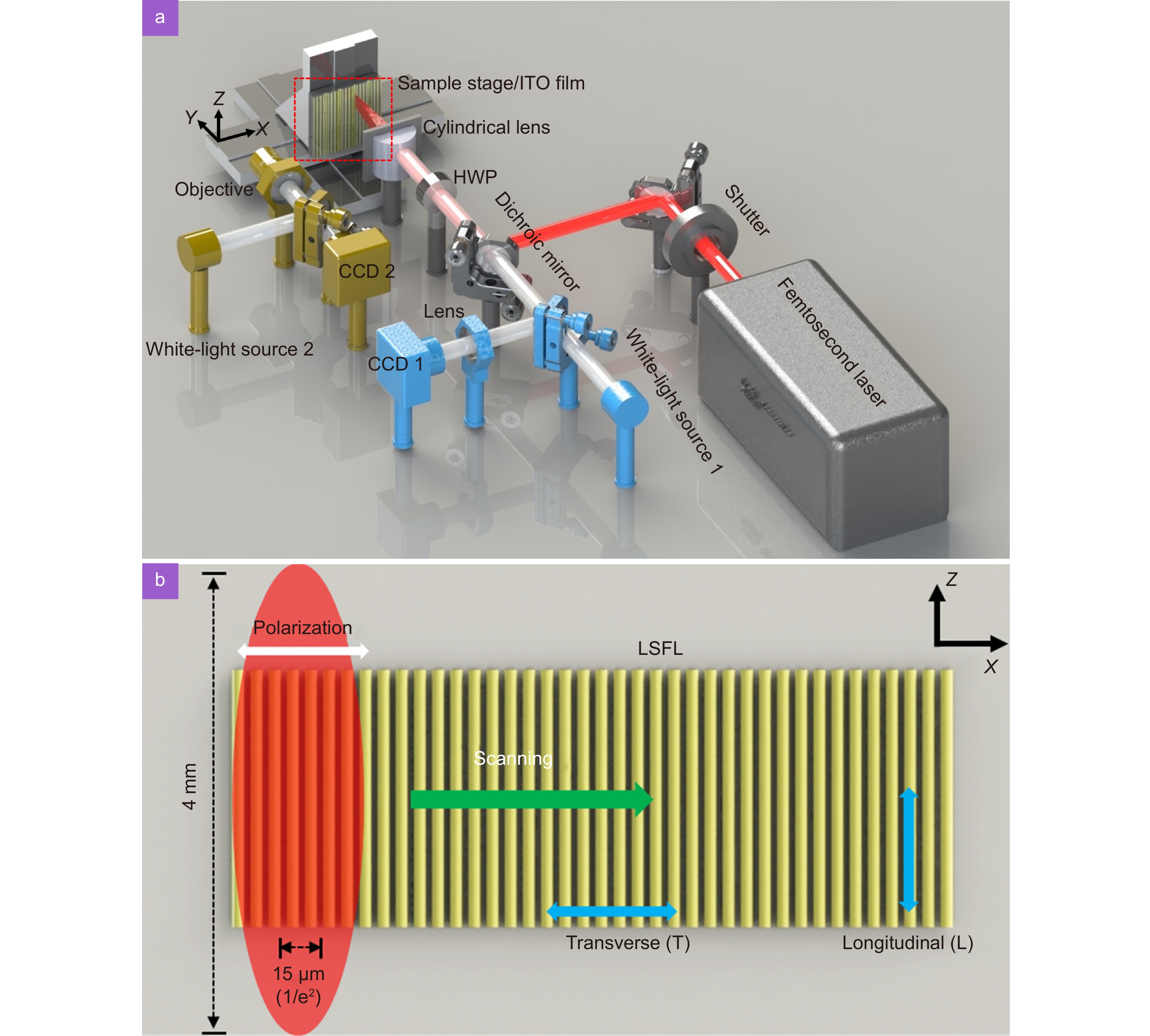
(a) Experimental system for direct writing of LIPSS in ITO films by a femtosecond laser. (b) Schematics of laser polarization, focal spot, scanning direction, transverse and longitudinal directions. HWP: half-wave plate, CCD: charge-coupled device.
-
Figure 2.
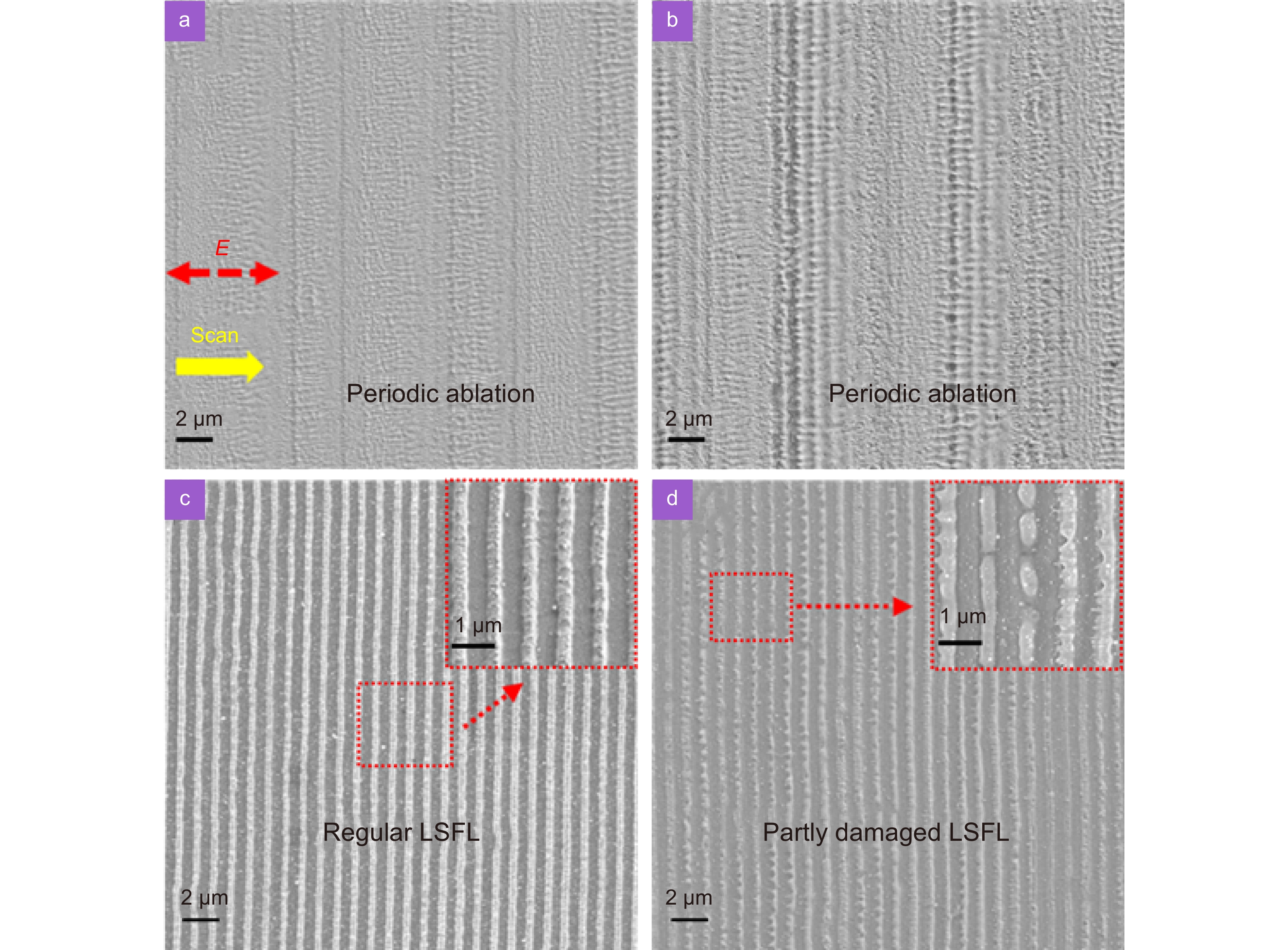
SEM images of ITO films irradiated by lasers with different fluences. (a) 0.212 J/cm2, (b) 0.446 J/cm2, (c) 0.531 J/cm2, and (d) 0.679 J/cm2. The inset shows an enlarged view of the area indicated by the red square. The scanning speed was 3 mm/s. The scanning direction and the direction of the electric field E are shown in (a).
-
Figure 3.
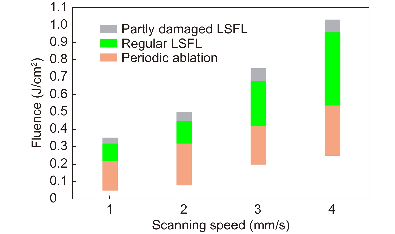
Laser fluences and scanning speeds for the three types of surface morphologies.
-
Figure 4.
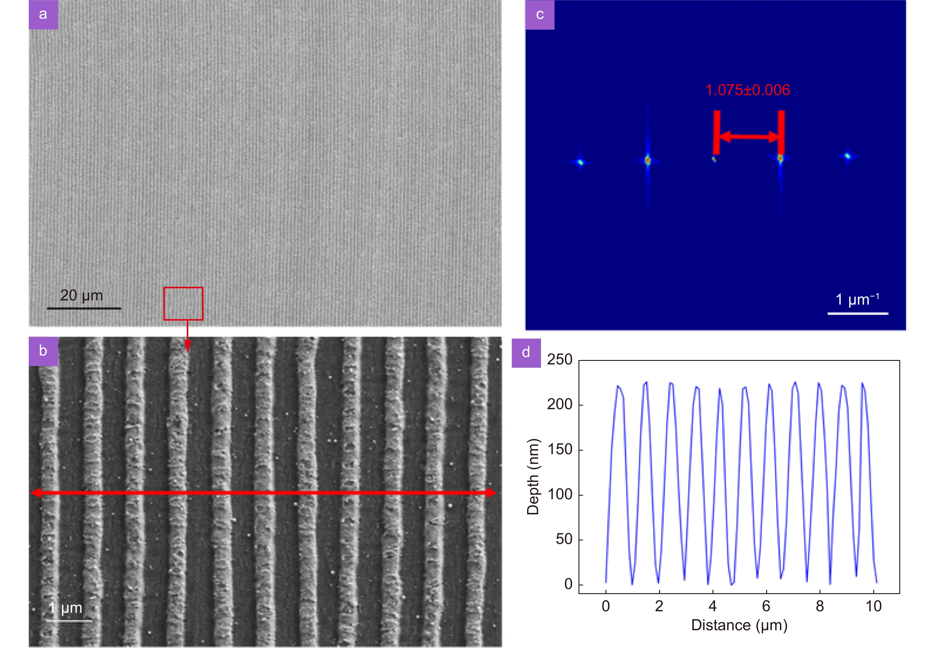
(a) SEM image of a large-area regular LSFL. (b) Enlarged image of the red square in (a). (c) Fourier transform image of (b). (d) Cross-sectional profile of the confocal optical micrograph of (b).
-
Figure 5.
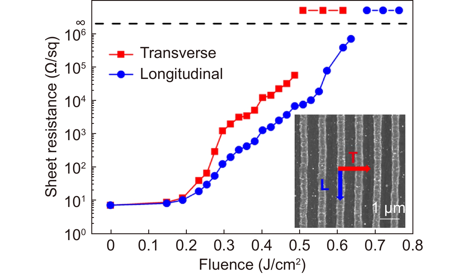
Sheet resistance of ITO film after laser direct writing with different fluences at a constant scanning speed of 3 mm/s.
-
Figure 6.
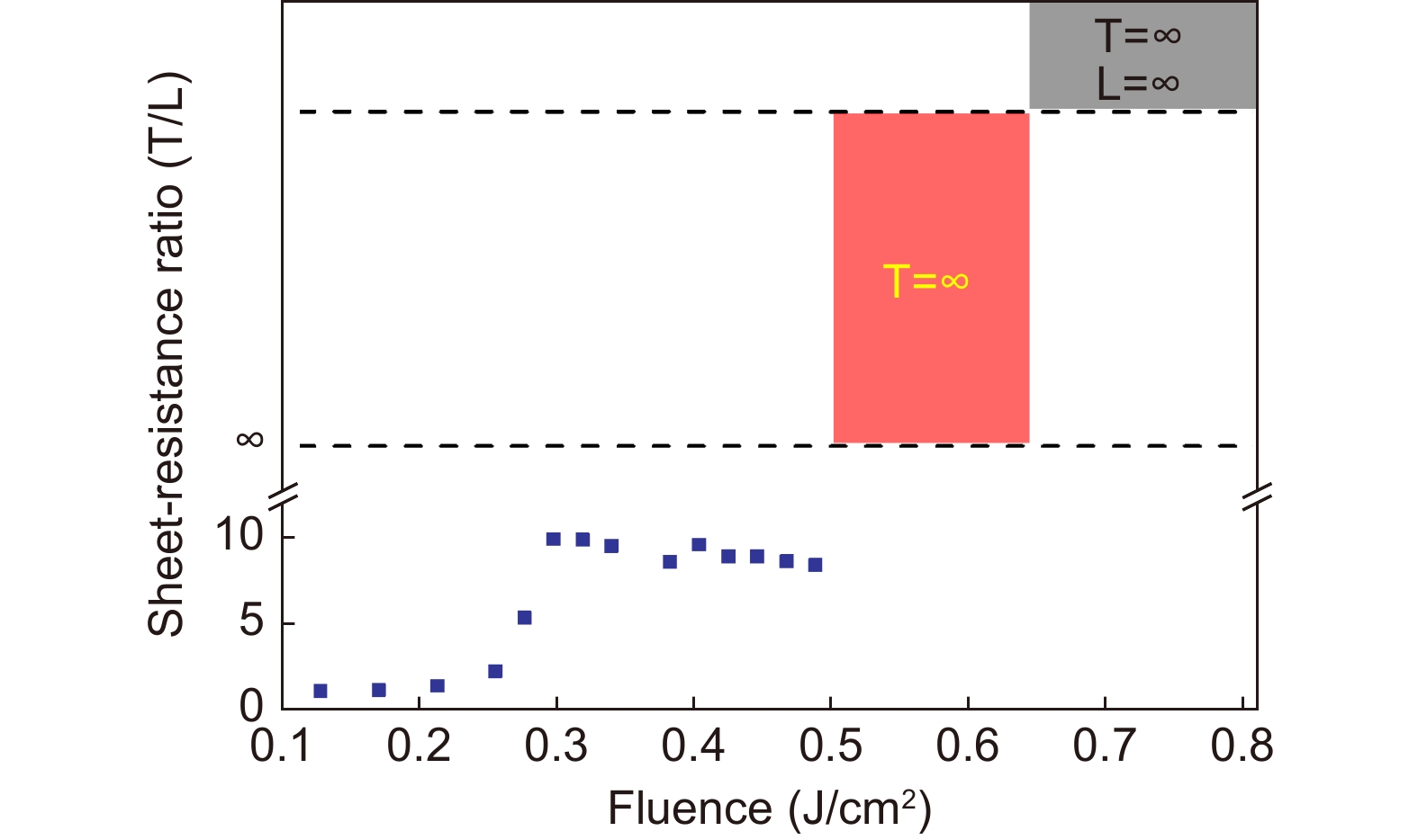
Ratio of the sheet resistance along the transverse (T) and longitudinal (L) directions with respect to the laser fluence at a constant scanning speed of 3 mm/s.
-
Figure 7.
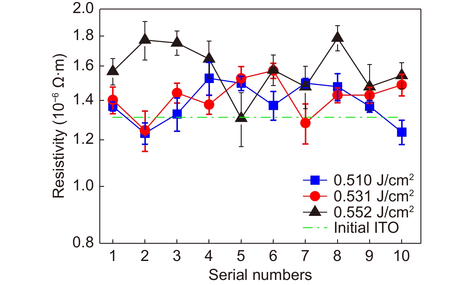
Resistivities of nanowires fabricated using lasers with different fluences.
-
Figure 8.
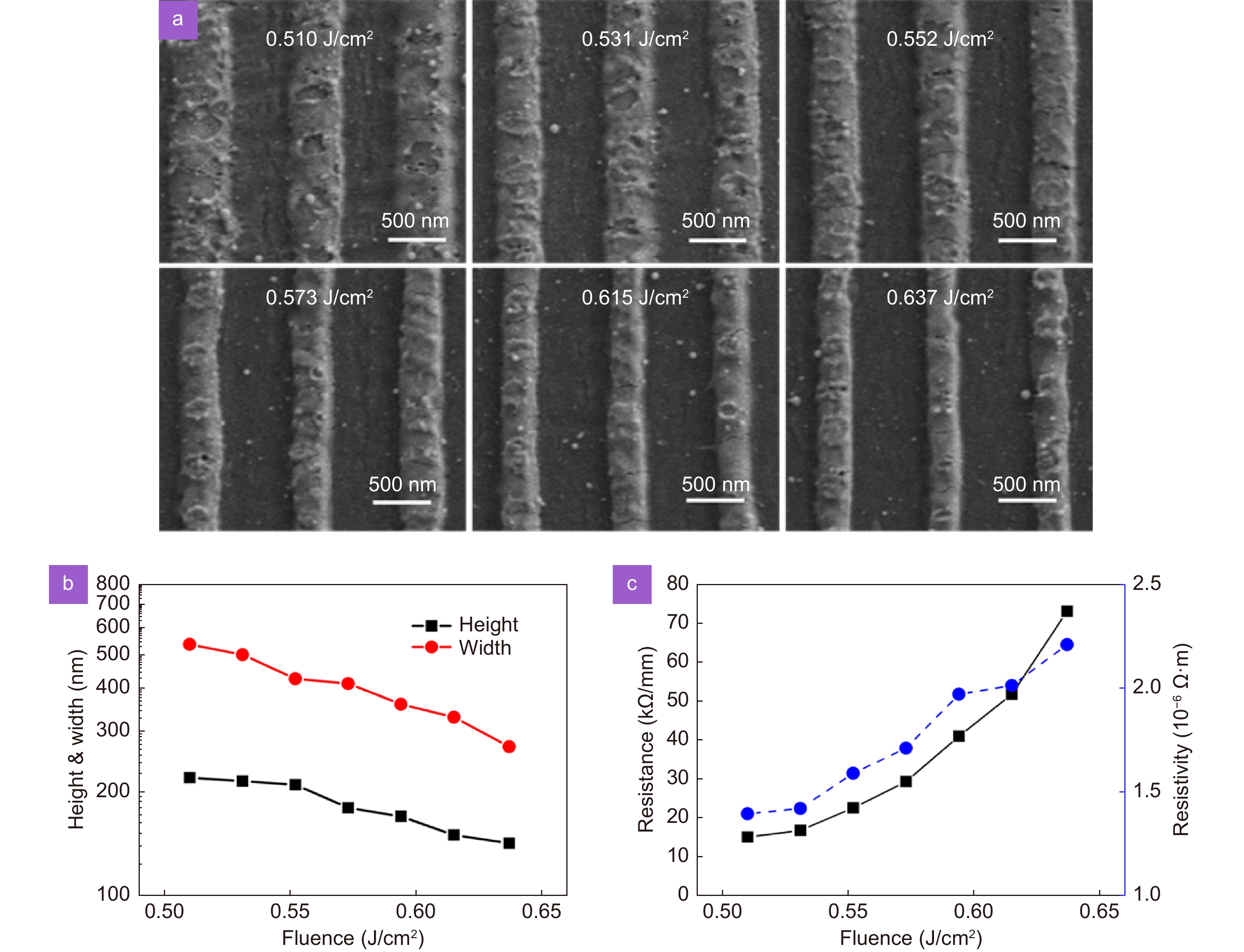
(a) SEM images of nanowires fabricated via laser direct writing with different fluences. (b) Height and width of nanowires with respect to the laser fluence. (c) Unit resistance and resistivity of nanowires with respect to the laser fluence.
-
Figure 9.
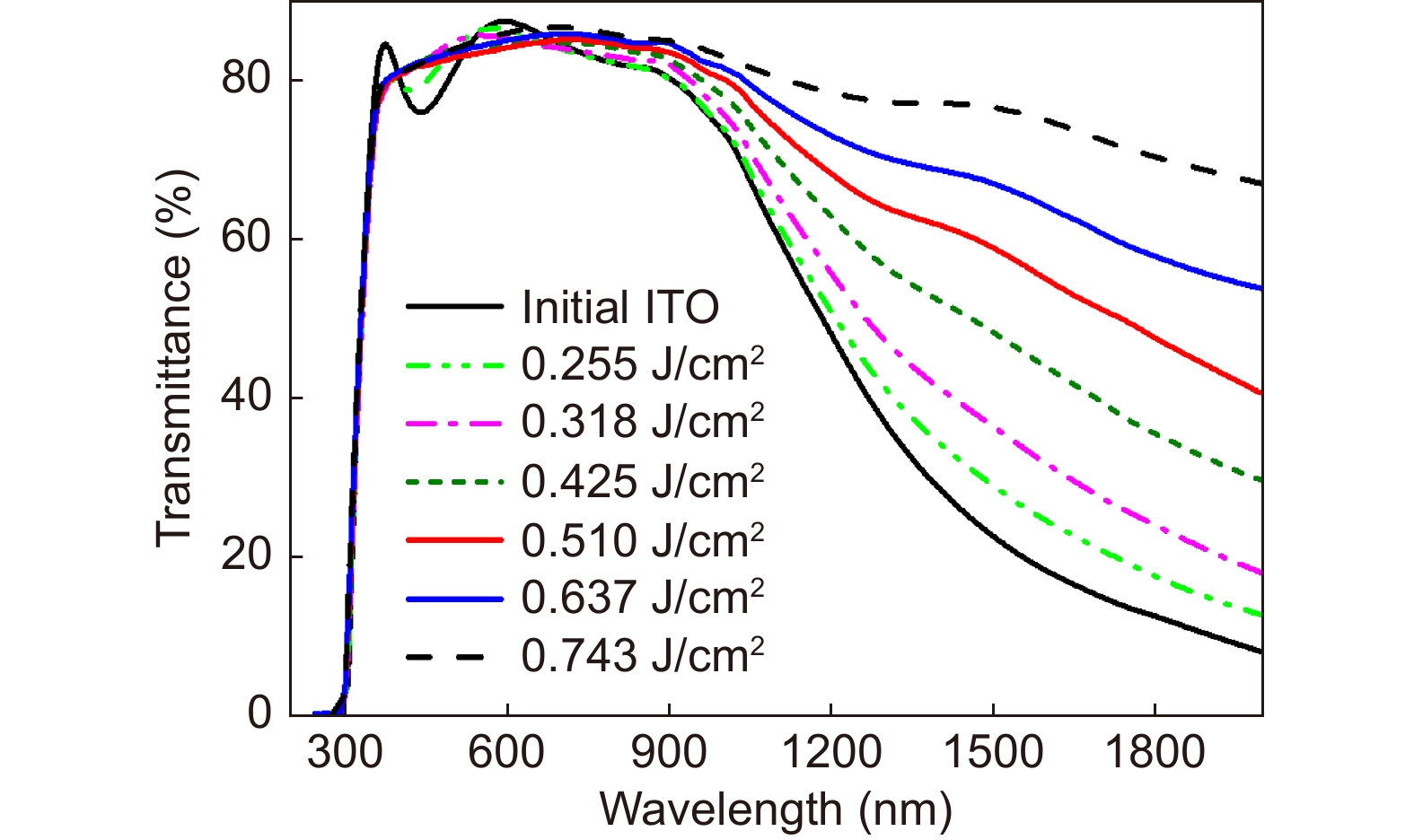
Transmission spectra of the ITO film after laser direct writing with different fluences at a constant scanning speed of 3 mm/s.
-
Figure 10.
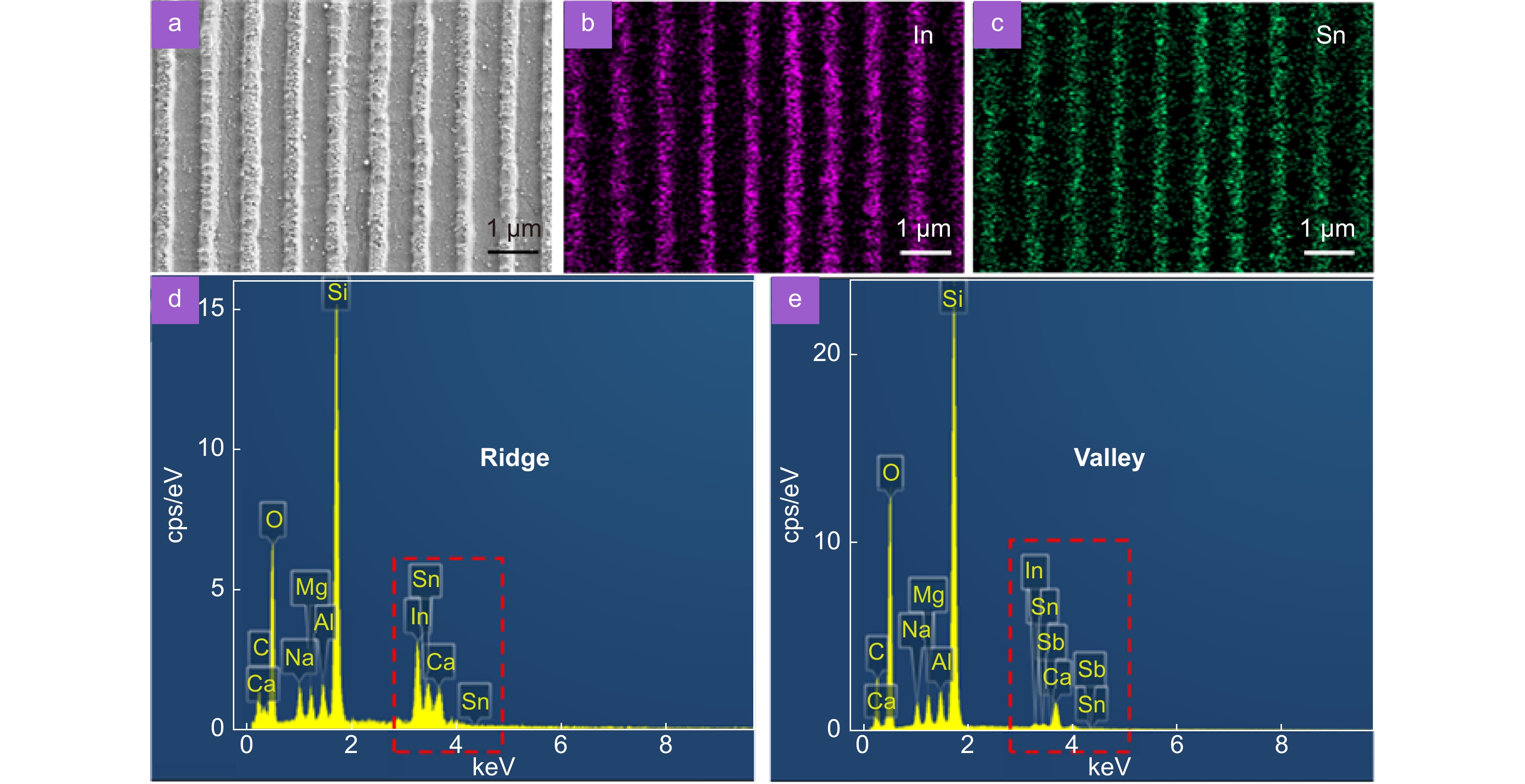
(a–c) Distributions of In and Sn for the ITO film with the LSFL; the scale bar represents 1 μm. Map sum spectra for the (d) ridge and (e) valley of the LSFL.
-
Figure 11.
Concentrations of In and Sn and the In/Sn ratio at the (a) ridge and (b) valley of the LSFL with respect to the laser fluence.
-
Figure 12.
(a) Distributions of In and Sn and (b) resistivity and sheet resistance for ITO films with different thicknesses.

 E-mail Alert
 RSS
RSS


 DownLoad:
