
 E-mail Alert
 RSS
RSS
| Citation: |

|
Light-triggered interfacial charge transfer and enhanced photodetection in CdSe/ZnS quantum dots/MoS2 mixed-dimensional phototransistors
-
Abstract
Mix-dimensional van der Waals heterostructures (vdWHs) have inspired worldwide interests and efforts in the field of advanced electronics and optoelectronics. The fundamental understanding of interfacial charge transfer is of vital importance for guiding the design of functional optoelectronic applications. In this work, type-II 0D-2D CdSe/ZnS quantum dots/MoS2 vdWHs are designed to study the light-triggered interfacial charge behaviors and enhanced optoelectronic performances. From spectral measurements in both steady and transient states, the phenomena of suppressed photoluminescence (PL) emissions, shifted Raman signals and changed PL lifetimes provide strong evidences of efficient charge transfer at the 0D-2D interface. A series of spectral evolutions of heterostructures with various QDs overlapping concentrations at different laser powers are analyzed in details, which clarifies the dynamic competition between exciton and trion during an efficient doping of 3.9×1013 cm−2. The enhanced photoresponses (1.57×10⁴ A·W–1) and detectivities (2.86×10¹¹ Jones) in 0D/2D phototransistors further demonstrate that the light-induced charge transfer is still a feasible way to optimize the performance of optoelectronic devices. These results are expected to inspire the basic understanding of interfacial physics at 0D/2D interfaces, and shed the light on promoting the development of mixed-dimensional optoelectronic devices in the near future.-
Keywords:
- heterostructure /
- phototransistor /
- MoS2 /
- quantum dots
-

-
References
[1] Zhang Z, Lin P, Liao QL, Kang Z, Si HN et al. Graphene-based mixed-dimensional van der Waals heterostructures for advanced optoelectronics. Adv Mater 31, 1806411 (2019). doi: 10.1002/adma.201806411 [2] Jariwala D, Marks TJ, Hersam MC. Mixed-dimensional van der Waals heterostructures. Nat Mater 16, 170–181 (2017). doi: 10.1038/nmat4703 [3] Zeng QS, Liu Z. Novel optoelectronic devices: transition-metal-dichalcogenide-based 2D heterostructures. Adv Electron Mater 4, 1700335 (2018). doi: 10.1002/aelm.201700335 [4] Hu C, Dong DD, Yang XK, Qiao KK, Yang D et al. Synergistic effect of hybrid PbS quantum dots/2D-WSe2 toward high performance and broadband phototransistors. Adv Funct Mater 27, 1603605 (2017). doi: 10.1002/adfm.201603605 [5] Song XF, Liu XH, Yu DJ, Huo CX, Ji JP et al. Boosting two-dimensional MoS2/CsPbBr3 photodetectors via enhanced light absorbance and interfacial carrier separation. ACS Appl Mater Interfaces 10, 2801–2809 (2018). doi: 10.1021/acsami.7b14745 [6] Yang TF, Wang X, Zheng BY, Qi ZY, Ma C et al. Ultrahigh-performance optoelectronics demonstrated in ultrathin perovskite-based vertical semiconductor heterostructures. ACS Nano 13, 7996–8003 (2019). doi: 10.1021/acsnano.9b02676 [7] Li F, Feng YX, Li ZW, Ma C, Qu JY et al. Rational kinetics control toward universal growth of 2D vertically stacked heterostructures. Adv Mater 31, 1901351 (2019). doi: 10.1002/adma.201901351 [8] Prins F, Goodman AJ, Tisdale WA. Reduced dielectric screening and enhanced energy transfer in single- and few-layer MoS2. Nano Lett 14, 6087–6091 (2014). doi: 10.1021/nl5019386 [9] Lin Z, Carvalho BR, Kahn E, Lv RT, Rao R et al. Defect engineering of two-dimensional transition metal dichalcogenides. 2D Mater 3, 22002 (2016). doi: 10.1088/2053-1583/3/2/022002 [10] Bertolazzi S, Bonacchi S, Nan GJ, Pershin A, Beljonne D et al. Engineering chemically active defects in monolayer MoS2 transistors via ion-beam irradiation and their healing via vapor deposition of alkanethiols. Adv Mater 29, 1606760 (2017). doi: 10.1002/adma.201606760 [11] Nguyen DA, Oh HM, Duong NT, Bang S, Yoon SJ et al. Highly enhanced photoresponsivity of a monolayer WSe2 photodetector with nitrogen-doped graphene quantum dots. ACS Appl Mater Interfaces 10, 10322–10329 (2018). doi: 10.1021/acsami.7b18419 [12] Li ZW, Liu CX, Rong X, Luo Y, Cheng HT et al. Tailoring MoS2 valley-polarized photoluminescence with super chiral near-field. Adv Mater 30, 1801908 (2018). doi: 10.1002/adma.201801908 [13] Li ZW, Li Y, Han TY, Wang XL, Yu Y et al. Tailoring MoS2 exciton-plasmon interaction by optical spin-orbit coupling. ACS Nano 11, 1165–1171 (2017). doi: 10.1021/acsnano.6b06834 [14] Ying HT, Li X, Wang HM, Wang YR, Hu X et al. Band structure engineering in MoS2 based heterostructures toward high-performance phototransistors. Adv Opt Mater 8, 2000430 (2020). doi: 10.1002/adom.202000430 [15] Hou HL, Zhang XW. Rational design of 1D/2D heterostructured photocatalyst for energy and environmental applications. Chem Eng J 395, 125030 (2020). doi: 10.1016/j.cej.2020.125030 [16] Konstantatos G, Badioli M, Gaudreau L, Osmond J, Bernechea M et al. Hybrid graphene–quantum dot phototransistors with ultrahigh gain. Nat Nanotech 7, 363–368 (2012). doi: 10.1038/nnano.2012.60 [17] Zheng DS, Wang JL, Hu WD, Liao L, Fang HH et al. When nanowires meet ultrahigh ferroelectric field−high-performance full-depleted nanowire photodetectors. Nano Lett 16, 2548–2555 (2016). doi: 10.1021/acs.nanolett.6b00104 [18] Luo WJ, Weng QC, Long MS, Wang P, Gong F et al. Room-temperature single-photon detector based on single nanowire. Nano Lett 18, 5439–5445 (2018). doi: 10.1021/acs.nanolett.8b01795 [19] Kufer D, Lasanta T, Bernechea M, Koppens FHL, Konstantatos G. Interface engineering in hybrid quantum dot–2D phototransistors. ACS Photonics 3, 1324–1330 (2016). doi: 10.1021/acsphotonics.6b00299 [20] Bessonov AA, Allen M, Liu YL, Malik S, Bottomley J et al. Compound quantum dot-perovskite optical absorbers on graphene enhancing short-wave infrared photodetection. ACS Nano 11, 5547–5557 (2017). doi: 10.1021/acsnano.7b00760 [21] Kagan CR, Lifshitz E, Sargent EH, Talapin DV. Building devices from colloidal quantum dots. Science 353, aac5523 (2016). doi: 10.1126/science.aac5523 [22] Wang HM, Li CH, Fang PF, Zhang ZL, Zhang JZ. Synthesis, properties, and optoelectronic applications of two-dimensional MoS2 and MoS2-based heterostructures. Chem Soc Rev 47, 6101–6127 (2018). doi: 10.1039/C8CS00314A [23] Subbaiah YPV, Saji KJ, Tiwari A. Atomically thin MoS2: a versatile nongraphene 2D material. Adv Funct Mater 26, 2046–2069 (2016). doi: 10.1002/adfm.201504202 [24] Cheng YC, Li HJW, Liu B, Jiang LY, Liu M et al. Vertical 0D-perovskite/2D-MoS2 van der Waals heterojunction phototransistor for emulating photoelectric-synergistically classical pavlovian conditioning and neural coding dynamics. Small 16, 2005217 (2020). doi: 10.1002/smll.202005217 [25] Wu HL, Kang Z, Zhang ZH, Zhang Z, Si HN et al. Interfacial charge behavior modulation in perovskite quantum dot-monolayer MoS2 0D-2D mixed-dimensional van der Waals heterostructures. Adv Funct Mater 28, 1802015 (2018). doi: 10.1002/adfm.201802015 [26] Wu HL, Si HN, Zhang ZH, Kang Z, Wu PW et al. All-inorganic perovskite quantum dot-monolayer MoS2 mixed-dimensional van der Waals heterostructure for ultrasensitive photodetector. Adv Sci 5, 1801219 (2018). doi: 10.1002/advs.201801219 [27] Zhang LW, Shen SL, Li M, Li LY, Zhang JB et al. Strategies for air-stable and tunable monolayer MoS2-based hybrid photodetectors with high performance by regulating the fully inorganic trihalide perovskite nanocrystals. Adv Opt Mater 7, 1801744 (2019). doi: 10.1002/adom.201801744 [28] Luo P, Zhuge FW, Wang FK, Lian LY, Liu KL et al. PbSe quantum dots sensitized high-mobility Bi2O2Se nanosheets for high-performance and broadband photodetection beyond 2 μm. ACS Nano 13, 9028–9037 (2019). doi: 10.1021/acsnano.9b03124 [29] Tang X, Lai KWC. Graphene/HgTe quantum-dot photodetectors with gate-tunable infrared response. ACS Appl Nano Mater 2, 6701–6706 (2019). doi: 10.1021/acsanm.9b01587 [30] Nikitskiy I, Goossens S, Kufer D, Lasanta T, Navickaite G et al. Integrating an electrically active colloidal quantum dot photodiode with a graphene phototransistor. Nat Commun 7, 11954 (2016). doi: 10.1038/ncomms11954 [31] Liu H, Wang C, Wang T, Hu XM, Liu DM et al. Controllable interlayer charge and energy transfer in perovskite quantum dots/transition metal dichalcogenide heterostructures. Adv Mater Interfaces 6, 1901263 (2019). doi: 10.1002/admi.201901263 [32] Zhang SK, Wang XD, Chen Y, Wu GJ, Tang YC et al. Ultrasensitive hybrid MoS2-ZnCdSe quantum dot photodetectors with high gain. ACS Appl Mater Interfaces 11, 23667–23672 (2019). doi: 10.1021/acsami.9b03971 [33] Ahn S, Chen WJ, Moreno-Gonzalez MA, Lockett M, Wang JY et al. Enhanced charge transfer and responsivity in hybrid quantum dot/graphene photodetectors using ZnO as intermediate electron-collecting layer. Adv Electron Mater 6, 2000014 (2020). doi: 10.1002/aelm.202000014 [34] Ye GL, Gong YJ, Lin JH, Li B, He YM et al. Defects engineered monolayer MoS2 for improved hydrogen evolution reaction. Nano Lett 16, 1097–1103 (2016). doi: 10.1021/acs.nanolett.5b04331 [35] Li SS, Lin YC, Zhao W, Wu J, Wang Z et al. Vapor-liquid-solid growth of monolayer MoS2 nanoribbons. Nat Mater 17, 535–542 (2018). doi: 10.1038/s41563-018-0055-z [36] Liu P, Zhu XQ, Feng C, Huang M, Li J et al. Enhanced p-type behavior in the hybrid structure of graphene quantum dots/2D-WSe2. Appl Phys Lett 111, 111603 (2017). doi: 10.1063/1.4989598 [37] Cho H, Jeong SH, Park MH, Kim YH, Wolf C et al. Overcoming the electroluminescence efficiency limitations of perovskite light-emitting diodes. Science 350, 1222–1225 (2015). doi: 10.1126/science.aad1818 [38] Ning ZJ, Gong XW, Comin R, Walters G, Fan FJ et al. Quantum-dot-in-perovskite solids. Nature 523, 324–328 (2015). doi: 10.1038/nature14563 [39] Cho IW, Ryu MY. Enhancement of luminescence properties and stability in perovskite hybrid structure with CdSe/ZnS quantum dots. APL Mater 7, 051112 (2019). doi: 10.1063/1.5097331 [40] Cho IW, Ryu MY. Effect of energy transfer on the optical properties of surface-passivated perovskite films with CdSe/ZnS quantum dots. Sci Rep 9, 18433 (2019). doi: 10.1038/s41598-019-54860-1 [41] Lanzafame JM, Miller RJD, Muenter AA, Parkinson BA. Ultrafast charge-transfer dynamics at tin disulfide surfaces. J Phys Chem 96, 2820–2826 (1992). doi: 10.1021/j100186a008 [42] Shi HY, Yan RS, Bertolazzi S, Brivio J, Gao B et al. Exciton dynamics in suspended monolayer and few-layer MoS2 2D crystals. ACS Nano 7, 1072–1080 (2013). doi: 10.1021/nn303973r [43] Liu B, Zhao WJ, Ding ZJ, Verzhbitskiy I, Li LJ et al. Engineering bandgaps of monolayer MoS2 and WS2 on fluoropolymer substrates by electrostatically tuned many-body effects. Adv Mater 28, 6457–6464 (2016). doi: 10.1002/adma.201504876 [44] Mak KF, He KL, Lee C, Lee GH, Hone J et al. Tightly bound trions in monolayer MoS2. Nat Mater 12, 207–211 (2013). doi: 10.1038/nmat3505 [45] Suh J, Park TE, Lin DY, Fu DY, Park J et al. Doping against the native propensity of MoS2: degenerate hole doping by cation substitution. Nano Lett 14, 6976–6982 (2014). doi: 10.1021/nl503251h [46] Ross JS, Wu SF, Yu HY, Ghimire NJ, Jones AM et al. Electrical control of neutral and charged excitons in a monolayer semiconductor. Nat Commun 4, 1474 (2013). doi: 10.1038/ncomms2498 [47] Mouri S, Miyauchi Y, Matsuda K. Tunable photoluminescence of monolayer MoS2 via chemical doping. Nano Lett 13, 5944–5948 (2013). doi: 10.1021/nl403036h [48] Li L, Wang WK, Chai Y, Li HQ, Tian ML et al. Few-layered PtS2 phototransistor on h-BN with high gain. Adv Funct Mater 27, 1701011 (2017). doi: 10.1002/adfm.201701011 [49] Island OJ, Blanter SI, Buscema M, van der Zant HSJ, Castellanos-Gomez A. Gate controlled photocurrent generation mechanisms in high-gain In2Se3 phototransistors. Nano Lett 15, 7853–7858 (2015). doi: 10.1021/acs.nanolett.5b02523 -
Supplementary Information
Supplementary information for Light-triggered interfacial charge transfer and enhanced photodetection in CdSe/ZnS quantum dots/MoS2 mixed-dimensional phototransistors 
-
Access History
Figures(5)
Article Metrics


Export File
Citation
Format
Content
 DownLoad:


-
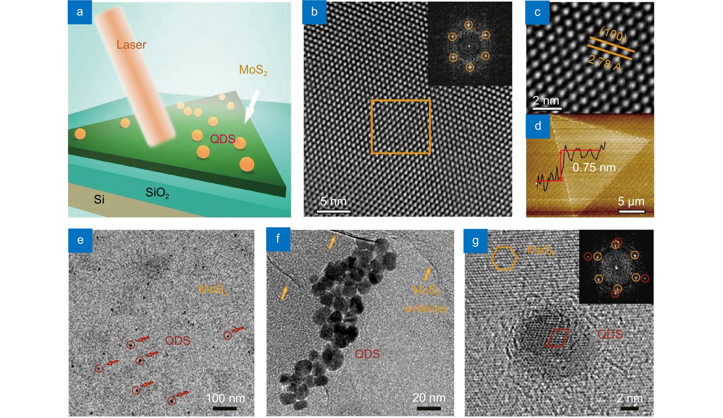
Figure 1.
Schematic view and TEM characterizations of MoS2 monolayer and CdSe/ZnS QDs. (a) Schematic view of mixed-dimensional QD/MoS2 heterostructures on SiO2/Si substrate under the excitation of a laser. (b) High-resolution TEM (HRTEM) image of MoS2 monolayer with the scale bar of 5 nm. The inset shows the corresponding selected area electron diffraction (SAED) pattern, where the diffraction points are arranged in a hexagonal structure. (c) Enlarged FFT image of the marked area in a rectangular region in (b). The lattice spacing is 2.78 Å. (d) The AFM image of MoS2 monolayer with clear surface, and the height of MoS2 is observed to be 0.75 nm. Low-resolution (e) and high-resolution (f) TEM images of QD/MoS2 heterostructures, where scale bars are 100 nm and 20 nm, respectively. The red arrows and circles in (e) are QDs on MoS2 monolayer, and the orange arrows in (f) are the wrinkles of MoS2 flakes. (g) The HRTEM image of QD/MoS2 structures with a scale bar of 2 nm. Inset shows two sets of SAED patterns.
-
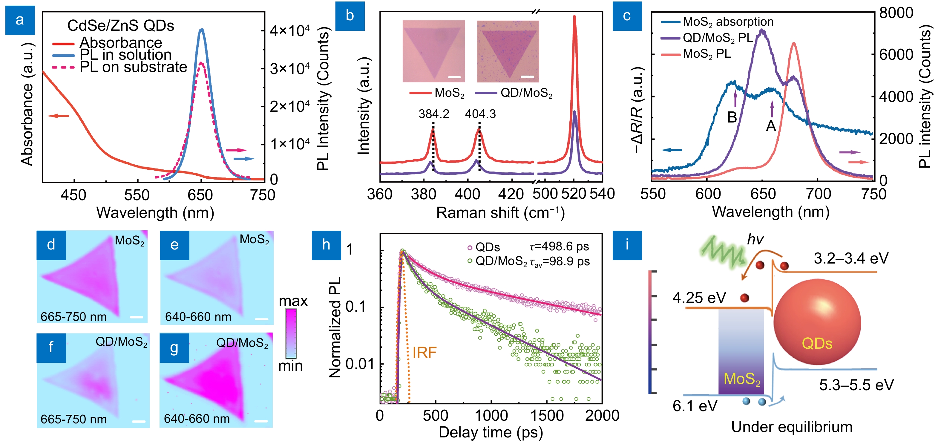
Figure 2.
Optical and spectral characteristics of QDs, MoS2 monolayer and mixed-dimensional vdWHs. (a) The UV-visible absorption spectrum (orange) of CdSe/ZnS QDs in 0.2 mg·L−1 solution. PL spectra of QDs in solution (blue) and on SiO2/Si substrate (dotted line). (b) Raman spectra of MoS2 monolayer and QD/MoS2 heterostructures. E12g and A1g modes are 384.2 cm−1 and 404.3 cm−1 for MoS2 monolayer, respectively, and the E12g peak shifts blue to 383.3 cm−1 in heterostructures. Insets present the optical microscopy images of MoS2 monolayer and heterostructure. The scale bars are 6 μm. (c) The absorption (black) and PL (red) spectra of MoS2 monolayer. The PL intensity maps of MoS2 monolayer are measured at the spectral ranges of (d) 665−750 nm and (e) 640−660 nm. The PL intensity maps of heterostructures with 0.025 mg·L−1 QDs are measured at the spectral ranges of (f) 665−750 nm and (g) 640−660 nm. All the scale bars in mapping images are 5 μm. (h) Time-resolved photoluminescence (TRPL) spectra of QDs and QD/MoS2 heterostructures. The average lifetimes of QDs and heterostrutures are 498.6 ps and 98.9 ps, respectively. (i) The schematic view of energy band for QD/MoS2 heterostructures under the light excitation.
-
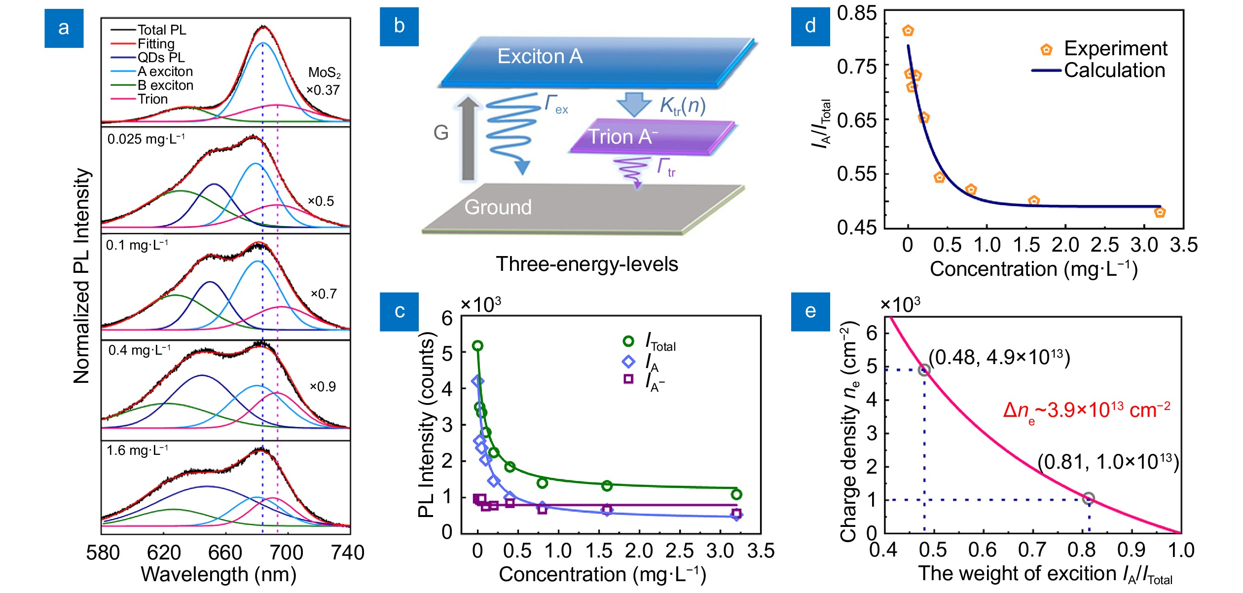
Figure 3.
Analysis of PL spectral evolution of heterostructures at various doping densities. (a) Normalized PL spectra of QD/MoS2 heterostructures with different QD concentrations. The total PL spectra (red) can be fitted well with several components, involving QD exciton (dark blue), MoS2 exciton A (blue), trion (pink) and exciton B (green). (b) Schematic view of the three-energy-levels including exciton, trion and ground states, where the trion is generated from the exciton. (c) Diagram of PL intensity of total intensity (ITotal), exciton (IA) and trion (IA-). Fitting curves match well with experimental results. (d) The weight ratio of exciton (IA/ITotal) as a function of concentration. (e) Calculations of charge density (ne) based on the law of mass action model. The electron density of charge transfer (Δne) is determined as 3.9×1013 cm−2.
-
Figure 4.
Laser-power dependent spectral modulation of QDs, MoS2 and their heterostructures. PL spectra change of (a) MoS2 monolayer and (b) QDs at various laser powers. (c) Analysis of PL spectral shapes in QD/MoS2 heterostructure with the excitation of various laser powers. The total PL peak consists of QD exciton (green), MoS2 exciton (A, blue), trion (A-, purple) and B exciton, and they can be fitted well in the shape of Lorentzian curves. (d) Plots of normalized PL intensity of exciton and trion as a function of laser powers. The relationship of PL intensity (I) and laser power (P) can be fitted as I=(P)m. (e) Schematic of exciton generation and emission at low and high laser powers.
-
Figure 5.
Optoelectronic performance of the vdWHs phototransistor compared with a pristine MoS2 phototransistor. (a) Schematic view of the phototransistor device, and the inset is an optical image of the as-prepared device with the scale bar of 10 μm. (b) Transfer characteristics of two devices in the dark and under the illuminations (from 0.11 nW to 34.75 nW) at Vds=1 V. (c) Transfer characteristics in dark (dotted line) and under the illumination (solid line, Peff = 34.7 nW) at Vg=0 V. (d) Photoresponsivities and (e) specific detectivities of two devices as a function of effective powers at Vg=60 V, respectively. (f) Time-dependent photoresponses under the pulsed illumination powers (from 0.11 nW to 19.78 nW) over multiple cycles at Vds=1 V. (g) The rise and fall times in photocurrent extracted from figure (f) under the illumination of 0.11 nW. (h) The photocurrent curves of vdWHs device with various QDs concentrations.


