
 E-mail Alert
 RSS
RSS
| Citation: |
Wu J, Qin F, Li X P. Atomically thin Fresnel zone plate with broadband focusing property[J]. Opto-Electron Eng, 2022, 49(4): 220011. doi: 10.12086/oee.2022.220011

|
Atomically thin Fresnel zone plate with broadband focusing property
-
Abstract
The planar diffractive lens in zone plate-type configuration plays important roles in the modern optical system, especially in the advanced optical imaging system. Most of them are constructed with opaque metal or dielectric materials with a high refractive index, which restricts the integration possibility for the miniaturized photonic systems. In this work, we proposed and experimentally demonstrated an atomic thin Fresnel zone plate device with 2D semiconductor material. Based on the loss-assisted phase modulation mechanism, an extraordinary phase modulation capability in the entire visible region has been achieved by an atomic thin MoS2 sheet. By utilizing the femtosecond laser scribing technique, a binary phase Fresnel zone plate has been fabricated on the atomic thin MoS2 sheet. The diffraction-limited focusing property in broadband has been demonstrated in simulation and experiments. Combining with the direct bandgap property of the monolayer MoS2 material, this phenomenon may pave the road for the integrated optical system.-
Keywords:
- 2D materials /
- phase singularity /
- loss-assisted /
- Fresnel zone plate /
- integrateable
-

-
References
[1] Di Fabrizio E, Romanato F, Gentili M, et al. High-efficiency multilevel zone plates for keV X-rays[J]. Nature, 1999, 401(6756): 895−898. doi: 10.1038/44791 [2] Liu T, Tan J B, Liu J, et al. Modulation of a super-Gaussian optical needle with high-NA Fresnel zone plate[J]. Opt Lett, 2013, 38(15): 2742−2745. doi: 10.1364/OL.38.002742 [3] Wang H T, Hao C L, Lin H, et al. Generation of super-resolved optical needle and multifocal array using graphene oxide metalenses[J]. Opto-Electron Adv, 2021, 4(2): 200031. [4] Wang J, Qin F, Zhang D H, et al. Subwavelength superfocusing with a dipole-wave-reciprocal binary zone plate[J]. Appl Phys Lett, 2013, 102(6): 061103. doi: 10.1063/1.4791581 [5] Rogers E T F, Lindberg J, Roy T, et al. A super-oscillatory lens optical microscope for subwavelength imaging[J]. Nat Mater, 2012, 11(5): 432−435. doi: 10.1038/nmat3280 [6] Wang Q, Rogers E T F, Gholipour B, et al. Optically reconfigurable metasurfaces and photonic devices based on phase change materials[J]. Nat Photonics, 2016, 10(1): 60−65. doi: 10.1038/nphoton.2015.247 [7] Qin F, Huang K, Wu J F, et al. A supercritical lens optical label‐free microscopy: sub‐diffraction resolution and ultra‐long working distance[J]. Adv Mater, 2017, 29(8): 1602721. doi: 10.1002/adma.201602721 [8] Tang D L, Wang C T, Zhao Z Y, et al. Ultrabroadband superoscillatory lens composed by plasmonic metasurfaces for subdiffraction light focusing[J]. Laser Photonics Rev, 2015, 9(6): 713−719. doi: 10.1002/lpor.201500182 [9] Wang C T, Tang D L, Wang Y Q, et al. Super-resolution optical telescopes with local light diffraction shrinkage[J]. Sci Rep, 2015, 5(1): 18485. doi: 10.1038/srep18485 [10] Huang K, Qin F, Liu H, et al. Planar diffractive lenses: fundamentals, functionalities, and applications[J]. Adv Mater, 2018, 30(26): 1704556. doi: 10.1002/adma.201704556 [11] Berry M, Zheludev N, Aharonov Y, et al. Roadmap on superoscillations[J]. J Opt, 2019, 21(5): 053002. doi: 10.1088/2040-8986/ab0191 [12] Fang W, Lei J, Zhang P D, et al. Multilevel phase supercritical lens fabricated by synergistic optical lithography[J]. Nanophoton, 2020, 9(6): 1469−1477. doi: 10.1515/nanoph-2020-0064 [13] Ouyang X, Xu Y, Xian M C, et al. Synthetic helical dichroism for six-dimensional optical orbital angular momentum multiplexing[J]. Nat Photonics, 2021, 15(12): 901−907. doi: 10.1038/s41566-021-00880-1 [14] Zhu L W, Cao Y Y, Chen Q Q, et al. Near-perfect fidelity polarization-encoded multilayer optical data storage based on aligned gold nanorods[J]. Opto-Electron Adv, 2021, 4(11): 210002. doi: 10.29026/oea.2021.210002 [15] Liu T, Shen T, Yang S M, et al. Subwavelength focusing by binary multi-annular plates: design theory and experiment[J]. J Opt, 2015, 17(3): 035610. doi: 10.1088/2040-8978/17/3/035610 [16] Liu T, Liu J, Zhang H, et al. Efficient optimization of super-oscillatory lens and transfer function analysis in confocal scanning microscopy[J]. Opt Commun, 2014, 319: 31−35. doi: 10.1016/j.optcom.2013.12.054 [17] Zhang Z X, Li Z Y, Lei J, et al. Environmentally robust immersion supercritical lens with an invariable sub-diffraction-limited focal spot[J]. Opt Lett, 2021, 46(10): 2296−2299. doi: 10.1364/OL.425361 [18] Huang K, Liu H, Garcia-Vidal F J, et al. Ultrahigh-capacity non-periodic photon sieves operating in visible light[J]. Nat Commun, 2015, 6(1): 7059. doi: 10.1038/ncomms8059 [19] Zhao X N, Hu J P, Lin Y, et al. Ultra-broadband achromatic imaging with diffractive photon sieves[J]. Sci Rep, 2016, 6(1): 28319. doi: 10.1038/srep28319 [20] Gao J, Yan S K, Zhou Y, et al. Polarization-conversion microscopy for imaging the vectorial polarization distribution in focused light[J]. Optica, 2021, 8(7): 984−994. doi: 10.1364/OPTICA.422836 [21] Fan Z B, Shao Z K, Xie M Y, et al. Silicon nitride metalenses for close-to-one numerical aperture and wide-angle visible imaging[J]. Phys Rev Appl, 2018, 10(1): 014005. doi: 10.1103/PhysRevApplied.10.014005 [22] Khorasaninejad M, Capasso F. Metalenses: versatile multifunctional photonic components[J]. Science, 2017, 358(6367): eaam8100. doi: 10.1126/science.aam8100 [23] Yang J, Wang Z, Wang F, et al. Atomically thin optical lenses and gratings[J]. Light Sci Appl, 2016, 5(3): e16046. doi: 10.1038/lsa.2016.46 [24] Liu C H, Zheng J J, Colburn S, et al. Ultrathin van der Waals metalenses[J]. Nano Lett, 2018, 18(11): 6961−6966. doi: 10.1021/acs.nanolett.8b02875 [25] Wang Z Y, Yang T S, Zhang Y P, et al. Flat lenses based on 2D perovskite nanosheets[J]. Adv Mater, 2020, 32(30): 2001388. doi: 10.1002/adma.202001388 [26] Li H, Zhang Q, Yap C C R, et al. From bulk to monolayer MoS2: evolution of Raman scattering[J]. Adv Funct Mater, 2012, 22(7): 1385−1390. doi: 10.1002/adfm.201102111 [27] Li Z W, Yang W, Huang M, et al. Light-triggered interfacial charge transfer and enhanced photodetection in CdSe/ZnS quantum dots/MoS2 mixed-dimensional phototransistors[J]. Opto-Electron Adv, 2021, 4(9): 210017. doi: 10.29026/oea.2021.210017 [28] Wang X D, Wang P, Wang J L, et al. Ultrasensitive and broadband MoS2 photodetector driven by ferroelectrics[J]. Adv Mater, 2015, 27(42): 6575−6581. doi: 10.1002/adma.201503340 [29] Radisavljevic B, Radenovic A, Brivio J, et al. Single-layer MoS2 transistors[J]. Nat Nanotechnol, 2011, 6(3): 147−150. doi: 10.1038/nnano.2010.279 [30] Mak K F, Lee C, Hone J, et al. Atomically thin MoS2: a new direct-gap semiconductor[J]. Phys Rev Lett, 2010, 105(13): 136805. doi: 10.1103/PhysRevLett.105.136805 [31] van de Groep J, Song J H, Celano U, et al. Exciton resonance tuning of an atomically thin lens[J]. Nat Photonics, 2020, 14(7): 426−430. doi: 10.1038/s41566-020-0624-y [32] Qin F, Liu B Q, Zhu L W, et al. π-phase modulated monolayer supercritical lens[J]. Nat Commun, 2021, 12(1): 32. doi: 10.1038/s41467-020-20278-x [33] Wang Y W, Deng Z L, Hu D J, et al. Atomically thin noble metal dichalcogenides for phase-regulated meta-optics[J]. Nano Lett, 2020, 20(11): 7811−7818. doi: 10.1021/acs.nanolett.0c01805 [34] Liu H L, Shen C C, Su S H, et al. Optical properties of monolayer transition metal dichalcogenides probed by spectroscopic ellipsometry[J]. Appl Phys Lett, 2014, 105(20): 201905. doi: 10.1063/1.4901836 -
Overview
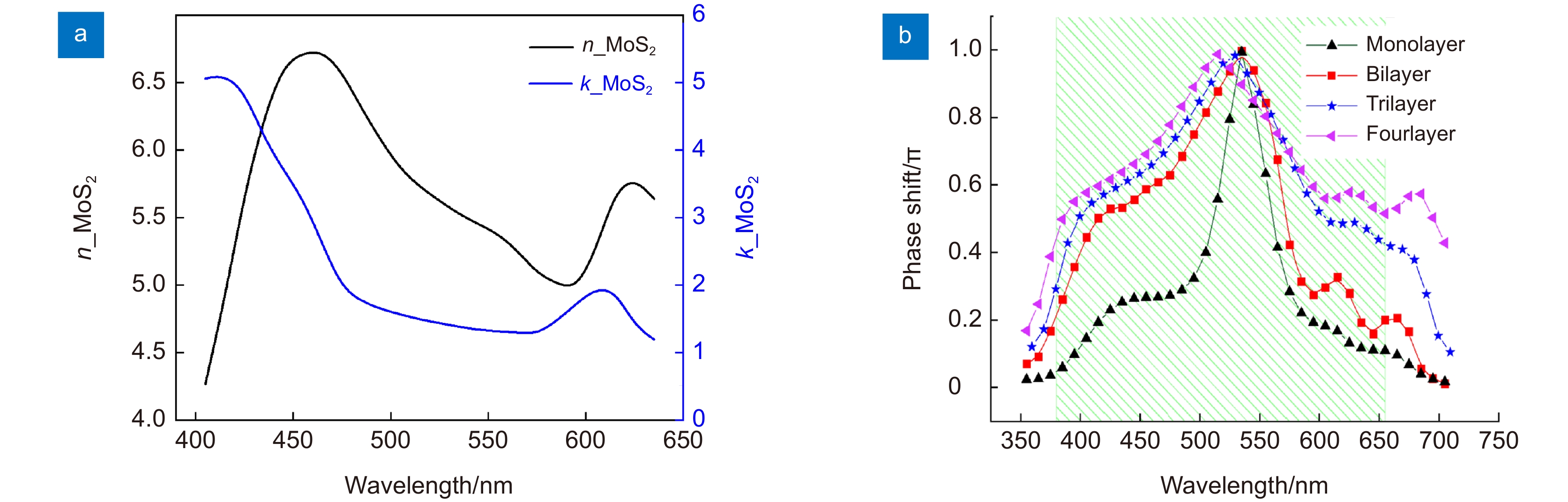
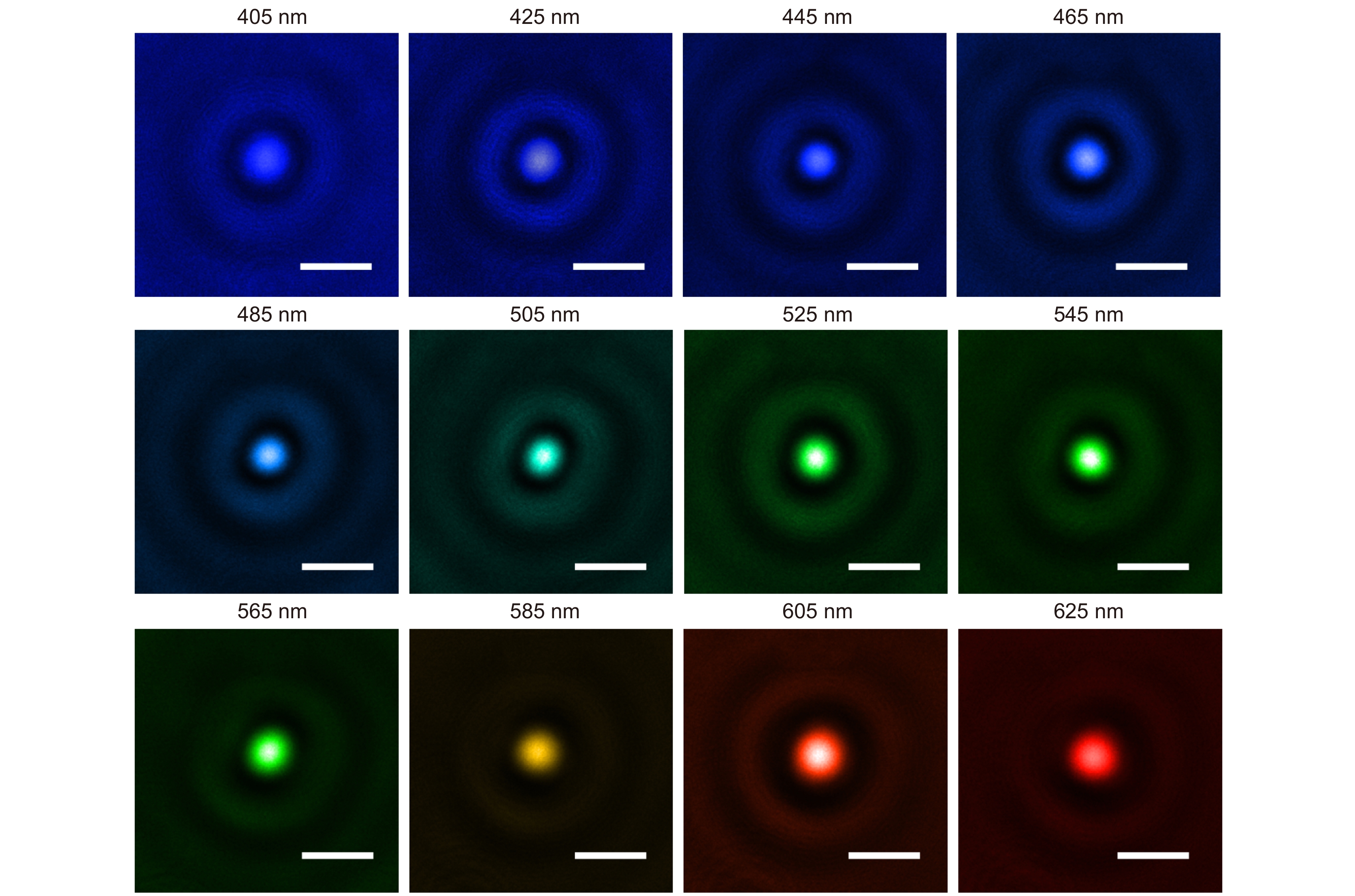
Although the diffractive lens with the photon-sieve and the metasurface metasurface type have been severely investigated in recently year, zone plate plate-type constructed with a series concentric phase and amplitude belts is still the most commonly used configuration, and have been frequently used in many applications including space telescope, high high-performance microscope object, projection illumination system, etc. Nevertheless, the integration possibility of such components in the opto-electronic circuits remains a challenge, due to the configuration of the incompatible materials configuration constructed with the opaque metal or dielectric materials with high refractive index. Two-dimensional transition -metal dichalcogenides (2D TMD) have attracted massive attention recently. As their typical representative, Molybdenum disulfide (MoS2) has been intensively investigated and shown extremely high quantum efficiency in photocurrent generation and photo-luminescence process owing to its unique photon-electronic characteristics. However, their capability for wavefront engineering has less been appreciated by far, due to the insufficient phase modulation capability when the thickness of the MoS2 sheet is decreased to atomic layers. In this work, we proposed and experimentally demonstrated an atomic thin Fresnel zone plate device. Based on the loss-assisted phase modulation mechanism, an extraordinary phase modulation of π phase shift for the optimized wavelength of 535 nm has been achieved by a monolayer MoS2 sheet with a thickness of 0.67 nm. Unlike the phase shift that comes from the dielectric or plasmonic resonator which highly rely relies on the spatial dimension of the resonator itself, the loss-assisted phase only determined by the basic configuration scheme has no obvious connection with the geometric size of the scribed pattern. Therefore, such an original phase shift mechanism can be applied for the creation of diffractive optical devices more conveniently. By utilizing the femtosecond laser scribing technique, a binary phase Fresnel zone plate has been fabricated on a monolayer and bilayer MoS2 sheet. The FZP is composed of 8 scribed concentric belts on the MoS2 sheet to form the alternating π and 0 phase zones between the scribed and un-scribed region. The radii of the zone belt are given by the standard FZP equation for satisfying the construction interference at the desired focal position. Experimentally measured results shown that a diffraction diffraction-limited focal spot with a focusing efficiency of around 5% has been obtained by the monolayer FZP device, which is notably outperforms the reported monolayer TMD lens with a focusing efficiency of 0.08%. Benefitting from the unique k dispersion property of the MoS2 sheet, such a significant phase modulation property could be extended to broadband through increasing the thickness of MoS2 from monolayer to bilayer. The simulation results shown that a 0.2π and above phase shift could be achieved in the wavelength region from blue to red light. The broadband focusing property have has been demonstrated in simulation and experiments from the wavelength of 405 nm to 635 nm. Combining with the direct bandgap property of the monolayer MoS2 material, this phenomenon may pave the road for the integrated opto-electronic system.
-
Access History
Figures(8)
Tables(1)
Article Metrics

Export File
Citation
Wu J, Qin F, Li X P. Atomically thin Fresnel zone plate with broadband focusing property[J]. Opto-Electron Eng, 2022, 49(4): 220011. doi: 10.12086/oee.2022.220011
Format
Content
 DownLoad:


-
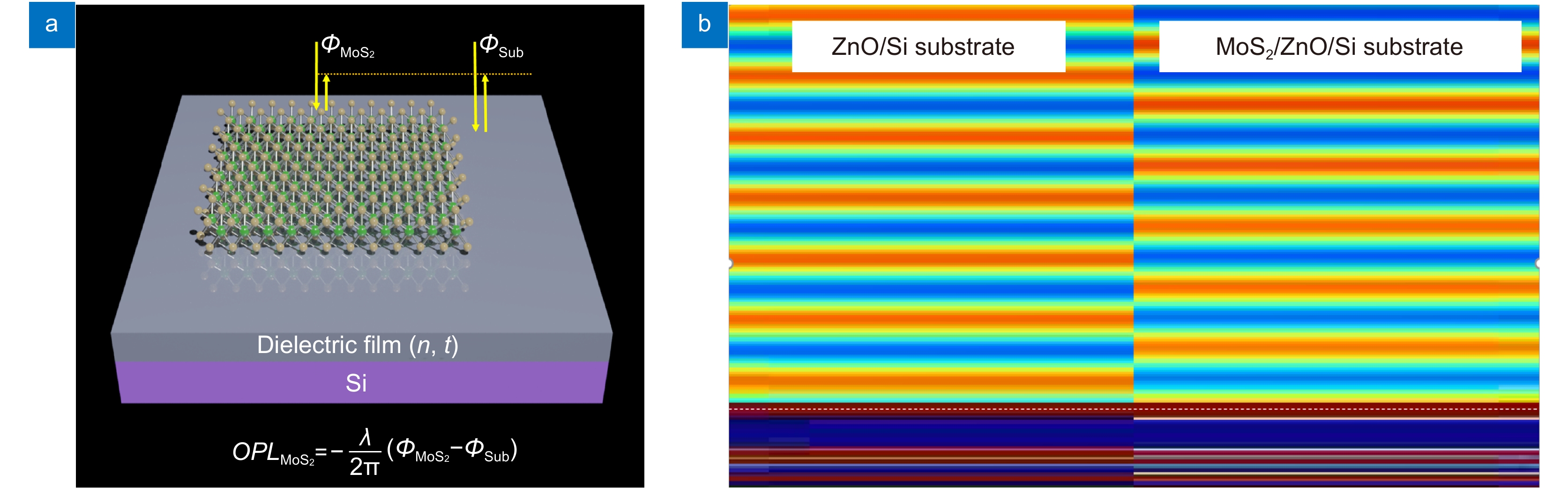
Figure 1.
Schematical shown of the loss-assisted phase shift mechanism.
-
Figure 2.
(a) The optical image; (b) SEM image; (c) Raman mapping image of the atomical thin Fresnel zone plate fabricated by laser scribing technique
-
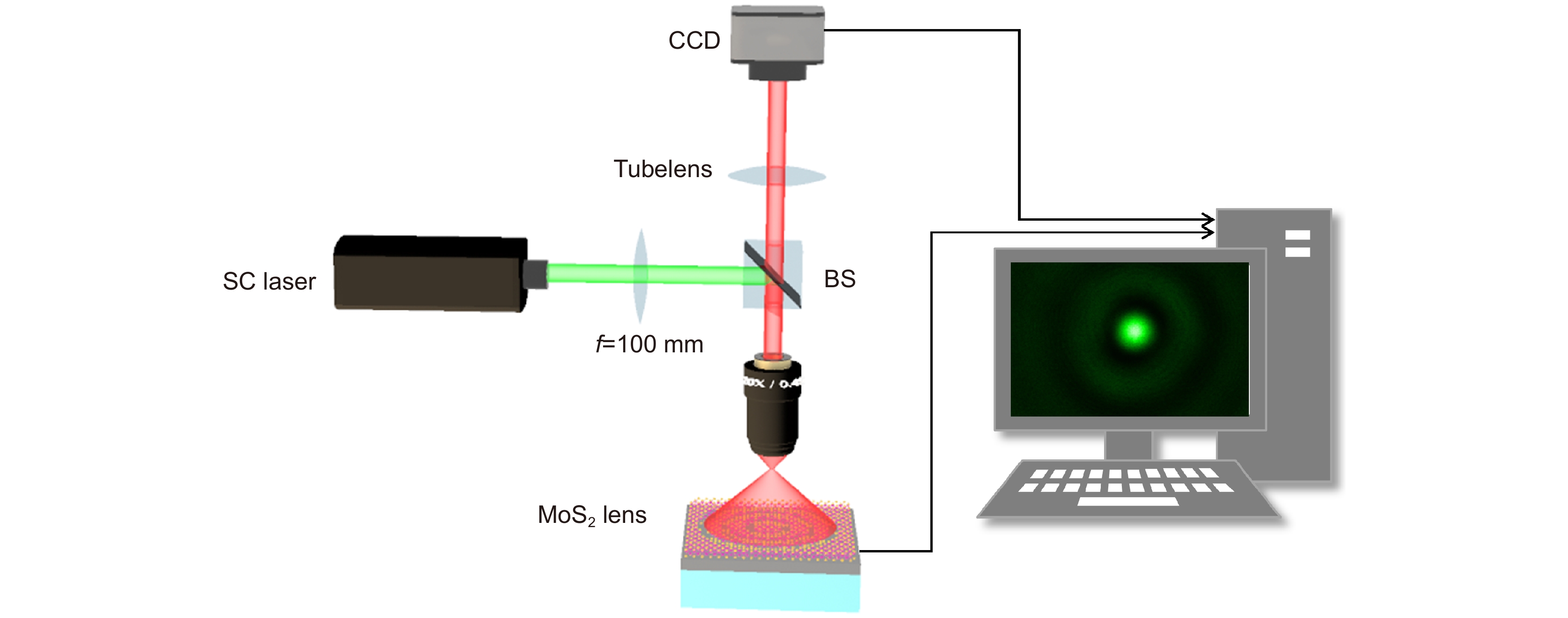
Figure 3.
Schematic diagram of the optical characterization system
-
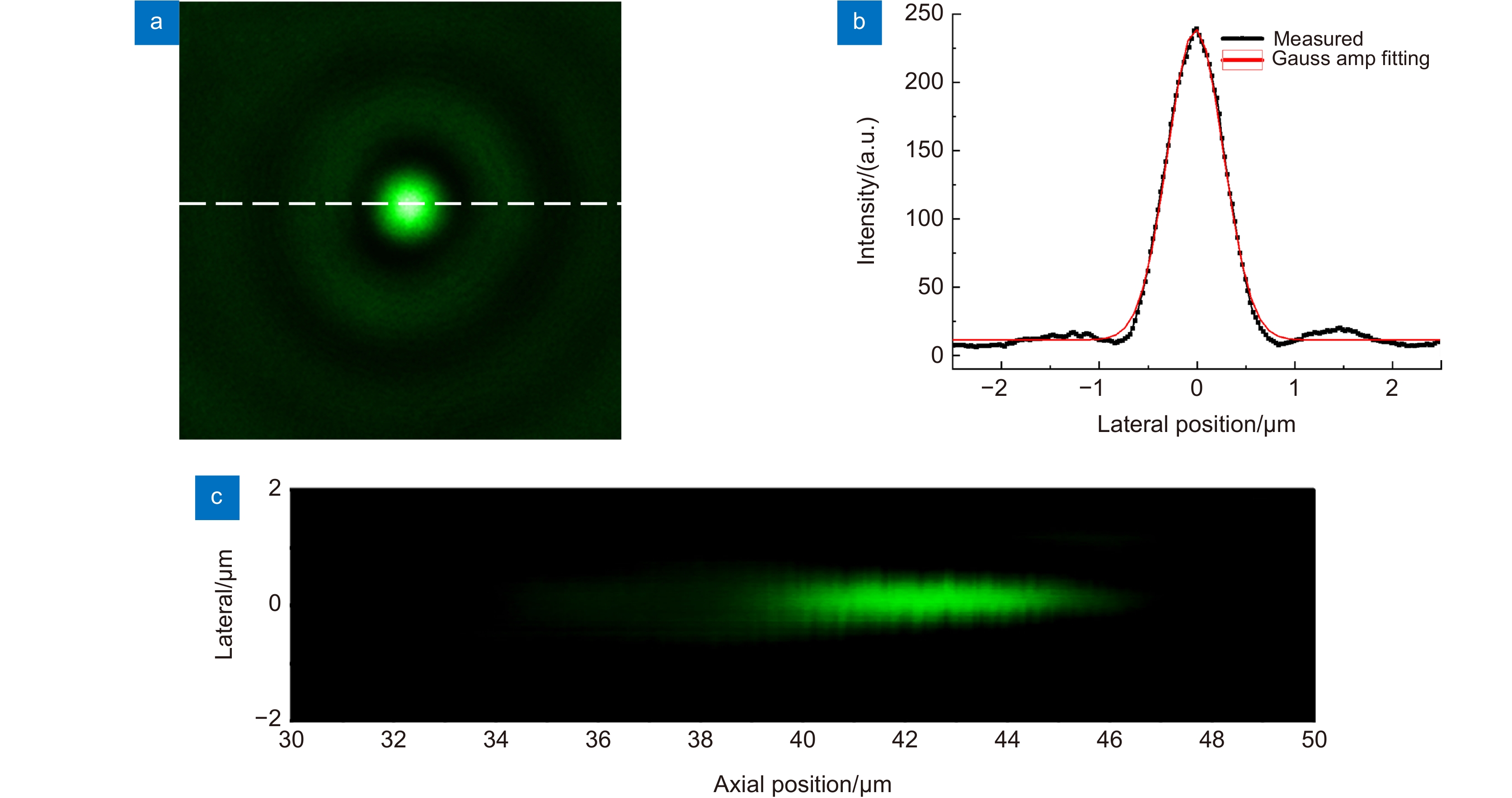
Figure 4.
The focusing property in 535 nm wavelength of the monolayer Fresnel zone plate.
-
Figure 5.
Broadband response of the phase modulation property of the 2D MoS2 sheet.
-
Figure 6.
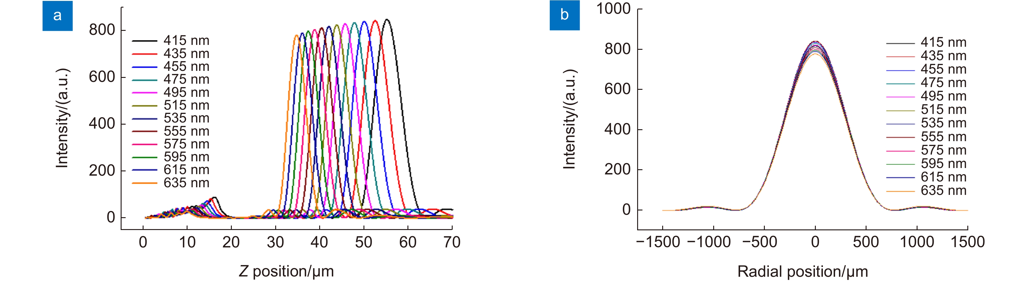
Simulation results of the broadband focusing properties.
-
Figure 7.
Measured broadband focusing property of the atomic thin planar diffractive lens.
- Figure .


