
 E-mail Alert
 RSS
RSS
| Citation: |

|
-
Abstract
In many application scenarios, silicon (Si) photonics favors the integration of III-V gain material onto Si substrate to realize the on-chip light source. In addition to the current popular integration approaches of III-V-on-Si wafer bonding or direct heteroepitaxial growth, a newly emerged promising solution of epitaxial regrowth on bonded substrate has attracted a lot of interests. High-quality III-V material realization and successful laser demonstrations show its great potential to be a promising integration platform for low-cost, high-integration density and highly scalable active-passive photonic integration on Si. This paper reviews recent research work on this regrowth on bonded template platform including template developments, regrown material characterizations and laser demonstrations. The potential advantages, opportunities and challenges of this approach are discussed.-
Keywords:
- Si photonics /
- III-V-on-Si laser /
- photonic integration /
- epitaxy regrowth
-

-
References
[1] Wirths S, Geiger R, von den Driesch N, Mussler G, Stoica T et al. Lasing in direct-bandgap GeSn alloy grown on Si. Nat Photon 9, 88–92 (2015). doi: 10.1038/nphoton.2014.321 [2] von den Driesch N, Stange D, Rainko D, Povstugar I, Zaumseil P et al. Advanced GeSn/SiGeSn group IV heterostructure lasers. Adv Sci 5, 1700955 (2018). doi: 10.1002/advs.201700955 [3] Margetis J, Zhou YY, Dou W, Grant PC, Alharthi B et al. All group-IV SiGeSn/GeSn/SiGeSn QW laser on Si operating up to 90 K. Appl Phys Lett 113, 221104 (2018). doi: 10.1063/1.5052563 [4] Lin SY, Zheng XZ, Yao J, Djordjevic SS, Cunningham JE et al. Efficient, tunable flip-chip-integrated III-V/Si hybrid external-cavity laser array. Opt Express 24, 21454–21462 (2016). doi: 10.1364/OE.24.021454 [5] Liang D, Roelkens G, Baets R, Bowers JE. Hybrid integrated platforms for silicon photonics. Materials 3, 1782–1802 (2010). doi: 10.3390/ma3031782 [6] Zhang C, Zhang SJ, Peters JD, Bowers JE. 8 × 8 × 40 Gbps fully integrated silicon photonic network on chip. Optica 3, 785–786 (2016). doi: 10.1364/OPTICA.3.000785 [7] Wang ZC, Tian B, Pantouvaki M, Guo WM, Absil P et al. Room-temperature InP distributed feedback laser array directly grown on silicon. Nat Photon 9, 837–842 (2015). doi: 10.1038/nphoton.2015.199 [8] Wang ZC, van Gasse K, Moskalenko V, Latkowski S, Bente E et al. A III-V-on-Si ultra-dense comb laser. Light Sci Appl 6, e16260 (2017). doi: 10.1038/lsa.2016.260 [9] Wirths S, Mayer B, Schmid H, Lörtscher E, Sousa M et al. Room temperature lasing from monolithically integrated GaAs microdisks on Si. In 2017 Conference on Lasers and Electro-Optics Europe & European Quantum Electronics Conference (IEEE, 2017); http://doi.org/10.1109/CLEOE-EQEC.2017.8086366. [10] Wirths S, Mayer BF, Schmid H, Sousa M, Gooth J et al. Room-temperature lasing from monolithically integrated GaAs microdisks on silicon. ACS Nano 12, 2169–2175 (2018). doi: 10.1021/acsnano.7b07911 [11] Mauthe S, Triviño NV, Baumgartner Y, Sousa M, Caimi D et al. InP-on-Si optically pumped microdisk lasers via monolithic growth and wafer bonding. IEEE J Sel Top Quantum Electron 25, 8300507 (2019). [12] Chen SM, Li W, Wu J, Jiang Q, Tang MC et al. Electrically pumped continuous-wave III–V quantum dot lasers on silicon. Nat Photon 10, 307–311 (2016). doi: 10.1038/nphoton.2016.21 [13] Liu AY, Zhang C, Norman J, Snyder A, Lubyshev D et al. High performance continuous wave 1.3 μm quantum dot lasers on silicon. Appl Phys Lett 104, 041104 (2014). doi: 10.1063/1.4863223 [14] Wan YT, Norman J, Li Q, Kennedy MJ, Liang D et al. 13 μm submilliamp threshold quantum dot micro-lasers on Si. Optica 4, 940–944 (2017). doi: 10.1364/OPTICA.4.000940 [15] Liu ST, Wu XR, Jung D, Norman JC, Kennedy MJ et al. High-channel-count 20 GHz passively mode-locked quantum dot laser directly grown on Si with 4.1 Tbit/s transmission capacity. Optica 6, 128–134 (2019). doi: 10.1364/OPTICA.6.000128 [16] Wan YT, Zhang S, Norman JC, Kennedy MJ, He W et al. Directly modulated single-mode tunable quantum dot lasers at 1.3 μm. Laser Photon Rev 14, 1900348 (2020). doi: 10.1002/lpor.201900348 [17] Wan YT, Norman JC, Tong YY, Kennedy MJ, He W et al. 1.3 μm quantum dot-distributed feedback lasers directly grown on (001) Si. Laser Photon Rev 14, 2000037 (2020). doi: 10.1002/lpor.202000037 [18] Jung D, Herrick R, Norman J, Turnlund K, Jan C et al. Impact of threading dislocation density on the lifetime of InAs quantum dot lasers on Si. Appl Phys Lett 112, 153507 (2018). doi: 10.1063/1.5026147 [19] Matsuo S, Takeda K, Sato T, Notomi M, Shinya A et al. Room-temperature continuous-wave operation of lateral current injection wavelength-scale embedded active-region photonic-crystal laser. Opt Express 20, 3773–3780 (2012). doi: 10.1364/OE.20.003773 [20] Matsuo S, Fujii T, Hasebe K, Takeda K, Sato T et al. Directly modulated buried heterostructure DFB laser on SiO2/Si substrate fabricated by regrowth of InP using bonded active layer. Opt Express 22, 12139–12147 (2014). doi: 10.1364/OE.22.012139 [21] Fujii T, Sato T, Takeda K, Hasebe K, Kakitsuka T et al. Epitaxial growth of InP to bury directly bonded thin active layer on SiO2/Si substrate for fabricating distributed feedback lasers on silicon. IET Optoelectron 9, 151–157 (2015). doi: 10.1049/iet-opt.2014.0138 [22] Nishi H, Fujii T, Diamantopoulos NP, Takeda K, Kanno E et al. Monolithic integration of an 8-channel directly modulated membrane-laser array and a SiN AWG Filter on Si. In 2018 Optical Fiber Communication Conference (OSA, 2018); http://doi.org/10.1364/ofc.2018.th3b.2 [23] Aihara T, Hiraki T, Fujii T, Takeda K, Tsuchizawa T et al. 56-Gbit/s operations of mach-zehnder modulators using 300-μm-long membrane InGaAsP phase shifters and SiN waveguides on Si. In 2019 Optical Fiber Communications Conference and Exhibition (IEEE, 2019); http://doi.org/10.1364/ofc.2019.m4a.3 [24] Sugiyama H, Nishiyama T, Kamada N, Onuki Y, Han X et al. Low threshold current of GaInAsP laser grown on directly bonded InP/Si substrate. In 2017 Conference on Lasers and Electro-Optics Pacific Rim (IEEE, 2017); http://doi.org/10.1109/CLEOPR.2017.8119024. [25] Periyanayagam GK, Nishiyama T, Kamada N, Onuki Y, Shimomura K. Lasing characteristics of 1.2 μm GaInAsP LD on InP/Si substrate. Phys Status Solidi (A) 215, 1700357 (2018). doi: 10.1002/pssa.201700357 [26] Tsushima K, Uchida K, Han X, Sugiyama H, Aikawa M et al. Lasing characteristics of GalnAsP SCH MQW high-mesa laser on silicon substrate. In 2019 24th OptoElectronics and Communications Conference (OECC) and 2019 International Conference on Photonics in Switching and Computing (IEEE, 2019); http://doi.org/10.23919/PS.2019.8818102. [27] Sugiyama H, Uchida K, Han X, Periyanayagam GK, Aikawa M et al. MOVPE grown GaInAsP/GaInAsP SCH-MQW laser diode on directly-bonded InP/Si substrate. J Cryst Growth 507, 93–97 (2019). doi: 10.1016/j.jcrysgro.2018.10.024 [28] Hu YT, Liang D, Zhang C, Kurczveil G, Huang X et al. Electrically-pumped 1.31 μm MQW lasers by direct epitaxy on wafer-bonded InP-on-SOI substrate. In 2018 IEEE Photonics Conference (IEEE, 2018); http://doi.org/10.1109/IPCon.2018.8527345 [29] Hu YT, Liang D, Mukherjee K, Li YL, Zhang C et al. III/V-on-Si MQW lasers by using a novel photonic integration method of regrowth on a bonding template. Light Sci Appl 8, 93 (2019). doi: 10.1038/s41377-019-0202-6 [30] Hu YT, Liang D, Kurczveil G, Beausoleil RG. A bonded template-assisted monolithic integration platform. Proc SPIE 11184, 111840O (2019). doi: 10.1117/12.2539077 [31] Besancon C, Vaissiere N, Dupré C, Fournel F, Sanchez L et al. Epitaxial growth of high-quality AlGaInAs-based active structures on a directly bonded InP-SiO2/Si substrate. Phys Status Solidi (A) 217, 1900523 (2020). doi: 10.1002/pssa.201900523 [32] Besancon C, Cerulo G, Néel D, Vaissiere N, Make D et al. Comparison of AlGaInAs-based laser behavior grown on hybrid InP-SiO2/Si and InP substrates. IEEE Photon Technol Lett 32, 469–472 (2020). doi: 10.1109/lpt.2020.2979254 [33] Liang D, Huang X, Kurczveil G, Fiorentino M, Beausoleil RG. Integrated finely tunable microring laser on silicon. Nat Photon 10, 719–722 (2016). doi: 10.1038/nphoton.2016.163 [34] Norman JC, Jung D, Zhang ZY, Wan YT, Liu ST et al. A review of high-performance quantum dot lasers on silicon. IEEE J Quantum Electron 55, 2000511 (2019). [35] Besancon C, Fanneau P, Néel D, Cerulo G, Vaissiere N et al. Laser array covering 155 nm wide spectral band achieved by selective area growth on silicon wafer. In 2020 European Conference on Optical Communications (IEEE, 2020); http://doi.org/10.1109/ECOC48923.2020.9333230. [36] Matsumoto K, Kishikawa J, Nishiyama T, Kanke T, Onuki Y et al. Room-temperature operation of GaInAsP lasers epitaxially grown on wafer-bonded InP/Si substrate. Appl Phys Express 9, 062701 (2016). doi: 10.7567/APEX.9.062701 [37] Kallarasan PG, Nishiyama T, Kamada N, Onuki Y, Shimomura K. 1.5μm laser diode on InP/Si substrate by epitaxial growth using direct bonding method. In 2017 Conference on Lasers and Electro-Optics (IEEE, 2017); http://doi.org/10.1364/CLEO_AT.2017.JTu5A.108. [38] Aihara T, Hiraki T, Takeda K, Hasebe K, Fujii T et al. Lateral current injection membrane buried heterostructure lasers integrated on 200-nm-thick Si waveguide. In 2018 Optical Fiber Communications Conference and Exposition (IEEE, 2018); http://doi.org/10.1364/ofc.2018.w3f.4. [39] Moscoso-Mártir A, Merget F, Mueller J, Hauck J, Romero-García S et al. Hybrid silicon photonics flip-chip laser integration with vertical self-alignment. In 2017 Conference on Lasers and Electro-Optics Pacific Rim (IEEE, 2017); http://doi.org/10.1109/CLEOPR.2017.8118971. [40] Zhang C, Bowers JE. Silicon photonic terabit/s network-on-chip for datacenter interconnection. Opt Fiber Technol 44, 2–12 (2018). doi: 10.1016/j.yofte.2017.12.007 [41] Huang R, Lan T, Li C, Li J, Wang ZY. Investigation of the blistering and exfoliation mechanism of GaAs wafers and SiO2/Si3N4/GaAs Wafers by He+ and H+ implantation. Crystals 10, 520 (2020). doi: 10.3390/cryst10060520 -
Access History
Figures(13)
Tables(2)
Article Metrics


Export File
Citation
Format
Content
 DownLoad:
-
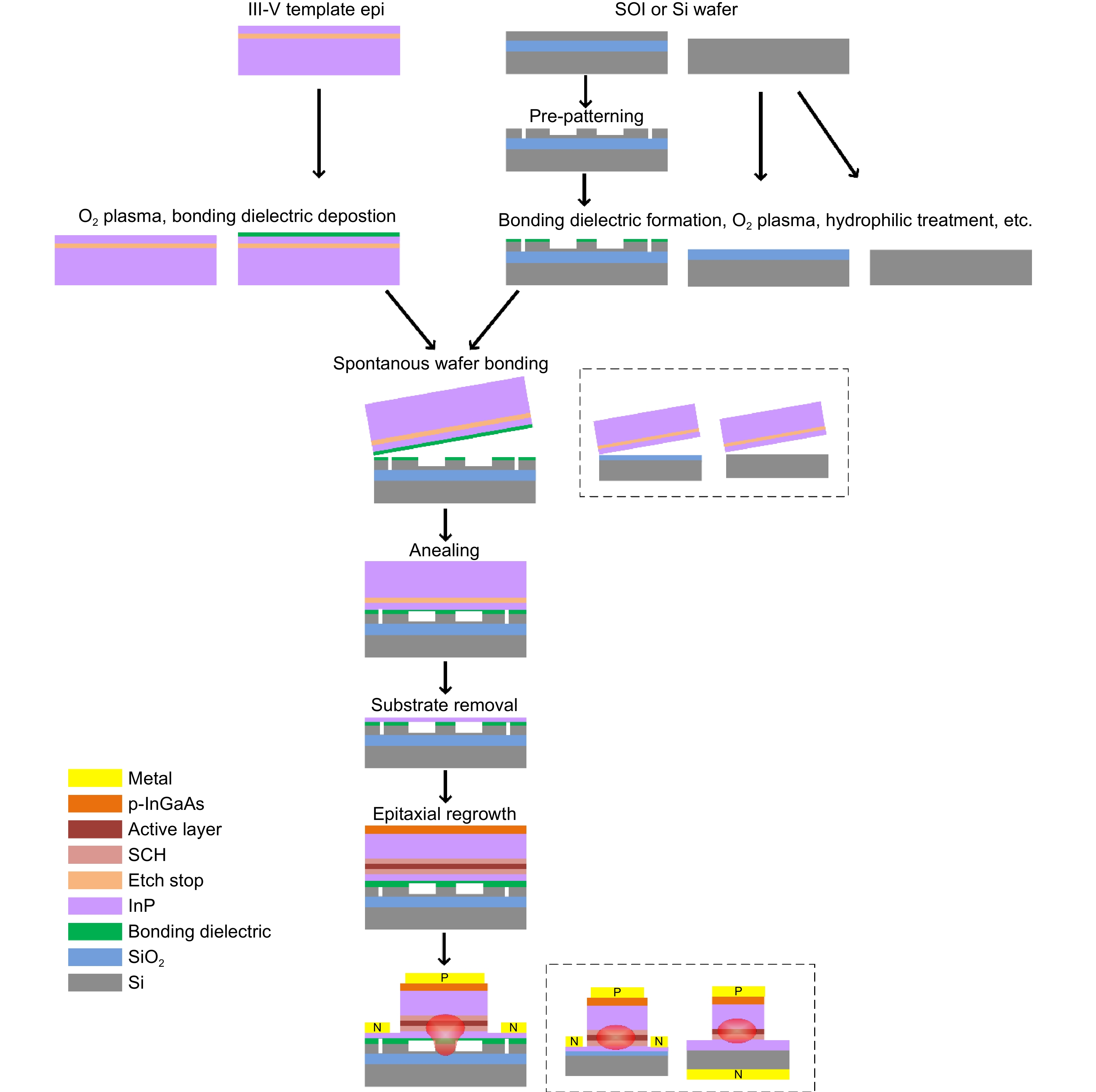
Figure 1.
A schematic drawing of the process flow for the advanced heterogeneous integration by using regrowth on III-V-on-Si bonding template.
-
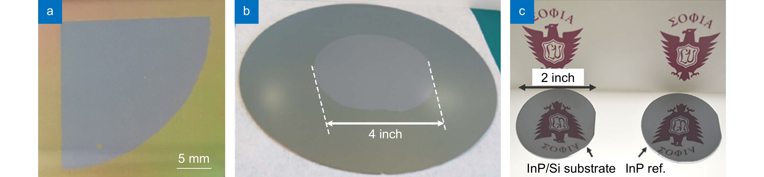
Figure 2.
Pictures of the fabricated InP-on-Si bonded wafers from HPE, III-V Lab and Sophia University. Figure repoduced with permisson from: (a) ref.29, under a Creative Commons Attribution 4.0 International License; (b) ref.31, (c) ref.25, John Wiley and Sons.
-
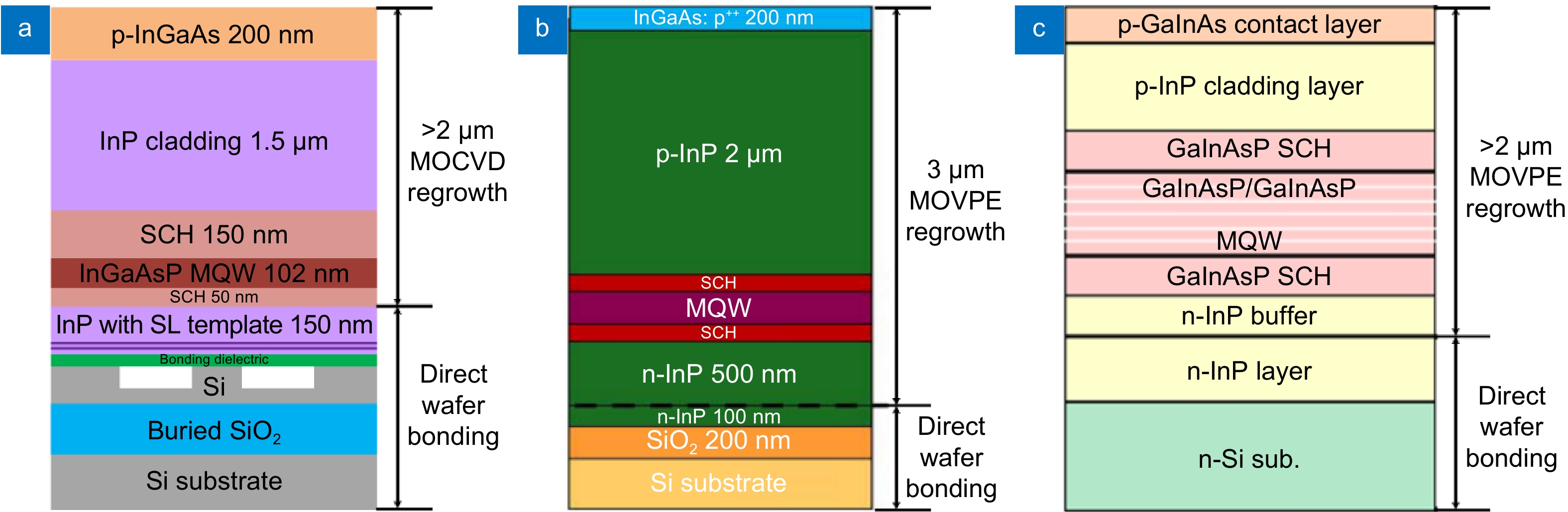
Figure 3.
Epitaxial regrowth laser structures on bonded templates from HPE, III-V Lab and Sophia University. Figure repoduced with permisson from: (a) ref.29, under a Creative Commons Attribution 4.0 International License; (b) ref.32, (c) ref.26, IEEE.
-
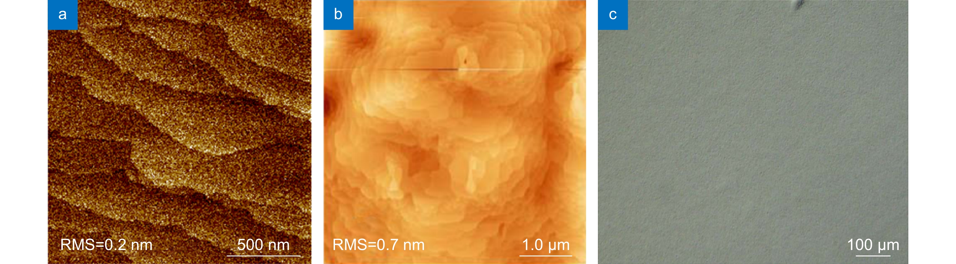
Figure 4.
AFM images and Nomarski microscope image of the epitaxial regrowth on bonded substrate from HPE, III-V Lab and Sophia University. Figure repoduced with permisson from: (a) ref.29,under a Creative Commons Attribution 4.0 International License; (b) ref.32, (c) ref.26, IEEE.
-
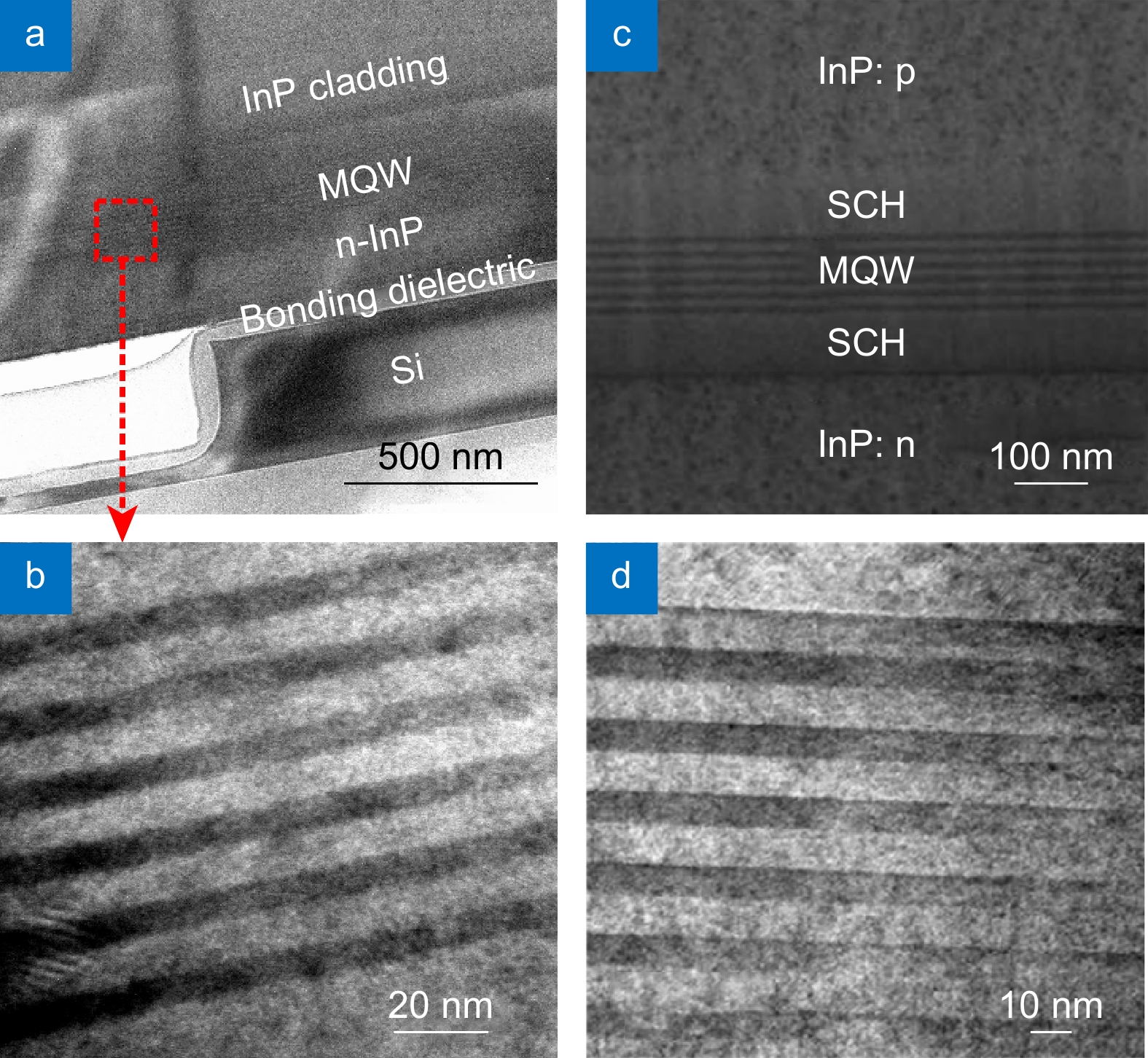
Figure 5.
Cross-sectional TEM (or STEM) images of the MQW or bulk epitaxy on the bonded substrate from HPE and III-V Lab. Figure repoduced with permisson from: (a, b) ref.29, under a Creative Commons Attribution 4.0 International License; (c) ref.32, IEEE; (d) ref.31, John Wiley and Sons.
-
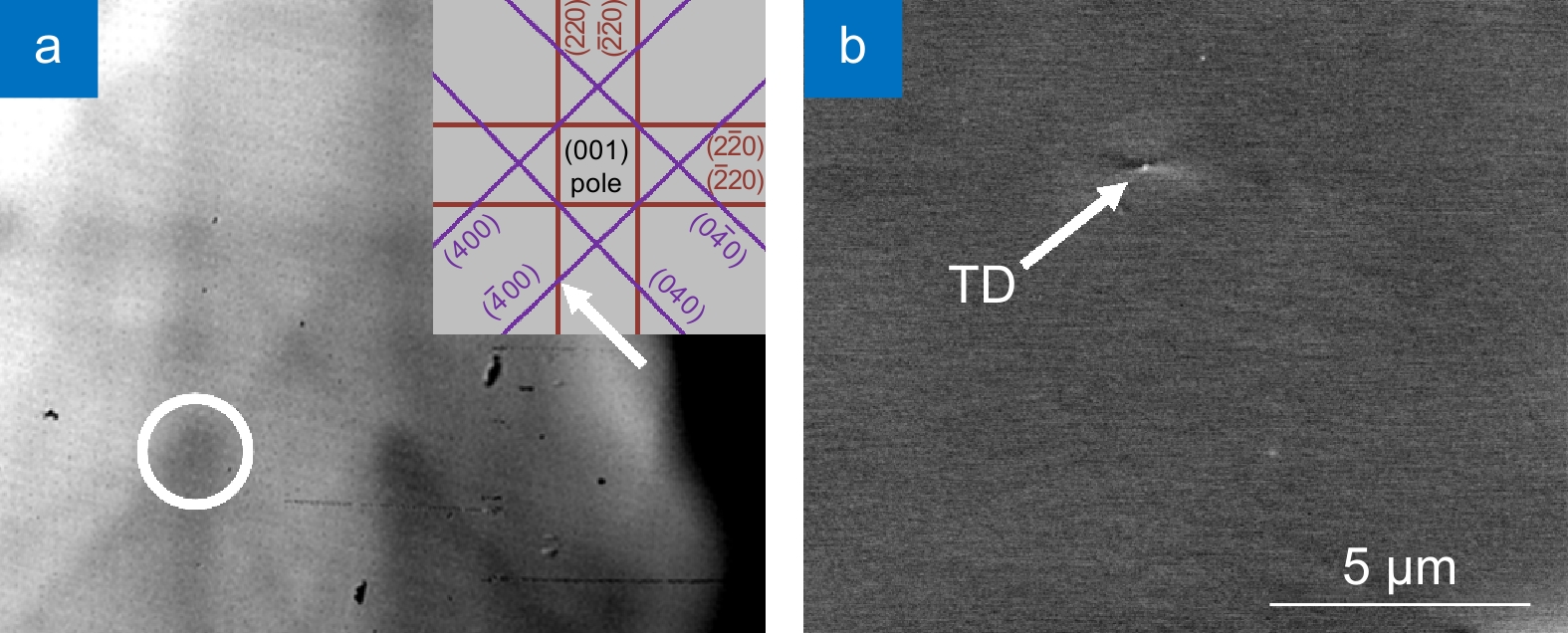
Figure 6.
(a) The electron channeling patterns corresponding to the three-beam (400) and (220) imaging conditions that were used in ECCI characterization. (b) A representative ECCI image with only one TD. Figure repoduced with permisson from ref.29, under a Creative Commons Attribution 4.0 International License.
-
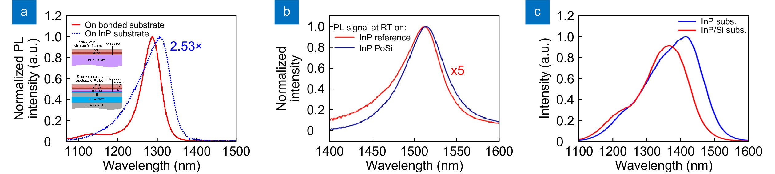
Figure 7.
The PL measurements at room temperature for the epitaxy on both InP and the bonded substrate from HPE, III-V Lab and Sophia University. Figure repoduced with permisson from: (a) ref.29, under a Creative Commons Attribution 4.0 International License; (b) ref.32, (c) ref.26, IEEE.
-
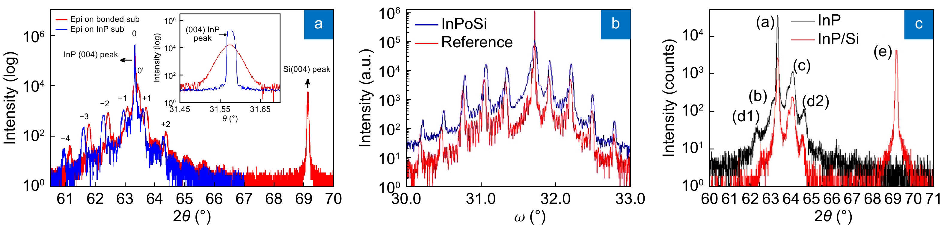
Figure 8.
XRD measurements on the epitaxy samples that from the three different research groups. Figure repoduced with permisson from: (a) ref.29, under a Creative Commons Attribution 4.0 International License; (b) ref.31, John Wiley and Sons; (c) ref.27, Elsevier.
-
Figure 9.
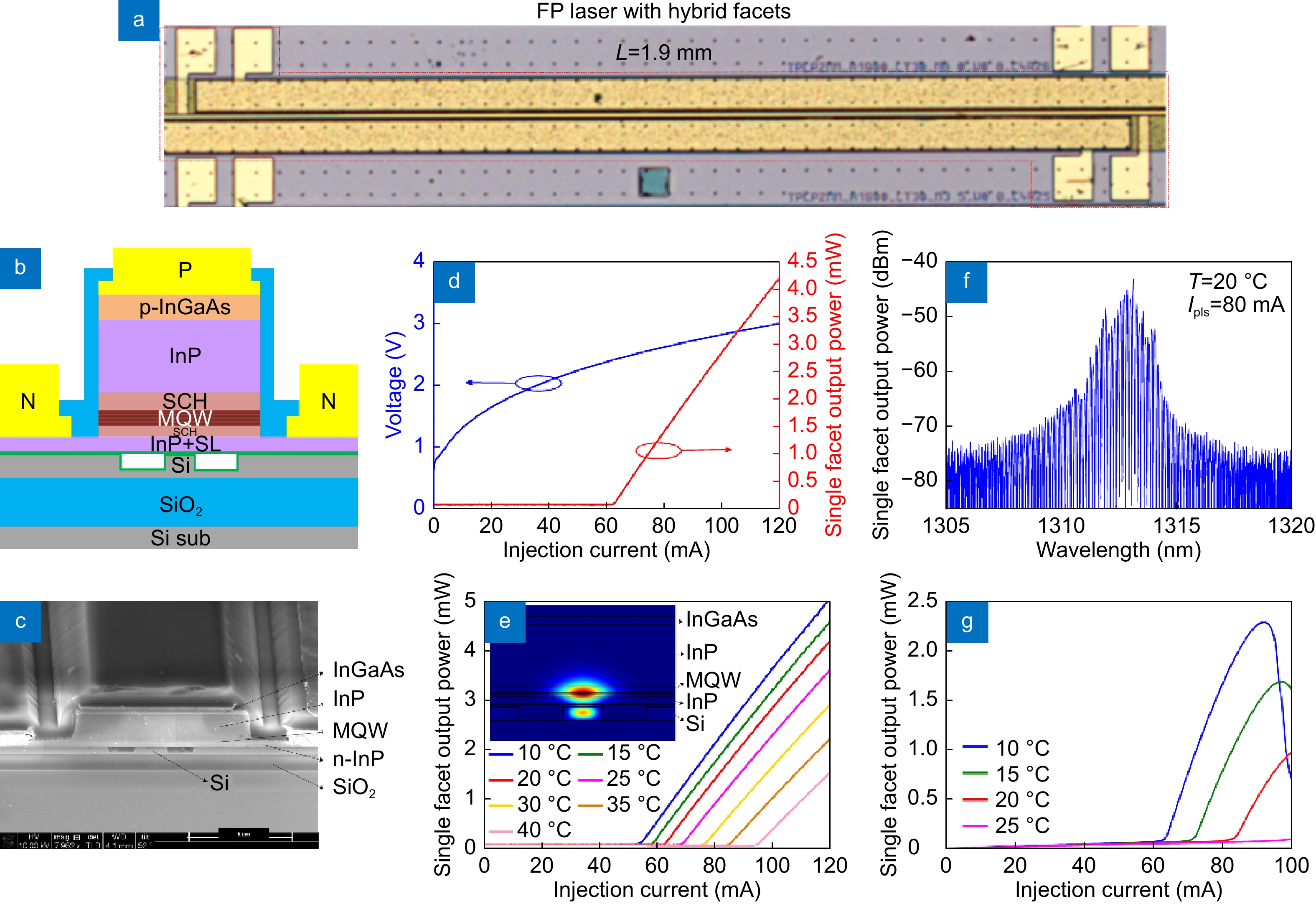
(a) A microscope image of a FP laser with hybrid facets. (b) Schematic drawing of the device cross-section and (c) SEM of the hybrid facet. (d) RT pulsed LIV. (e) Pulsed LI up to 40 °C (inset: mode profile at facets). (f) Device spetrum. (g) cw LI up to 25 °C. Figure repoduced with permisson from ref.29, under a Creative Commons Attribution 4.0 International License.
-
Figure 10.
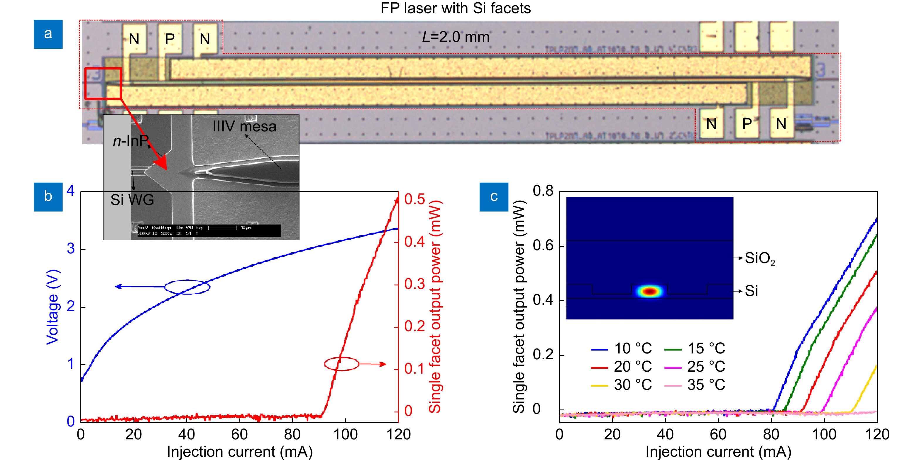
(a) A microscope image of a FP laser with Si waveguide facets and a SEM image of a III/V-to-Si taper. (b) RT pulsed LIV (inset: microscope image of the device), (c) pulsed LI up to 40 °C (inset: mode profile at facets). Figure repoduced with permisson from ref.29, under a Creative Commons Attribution 4.0 International License.
-
Figure 11.
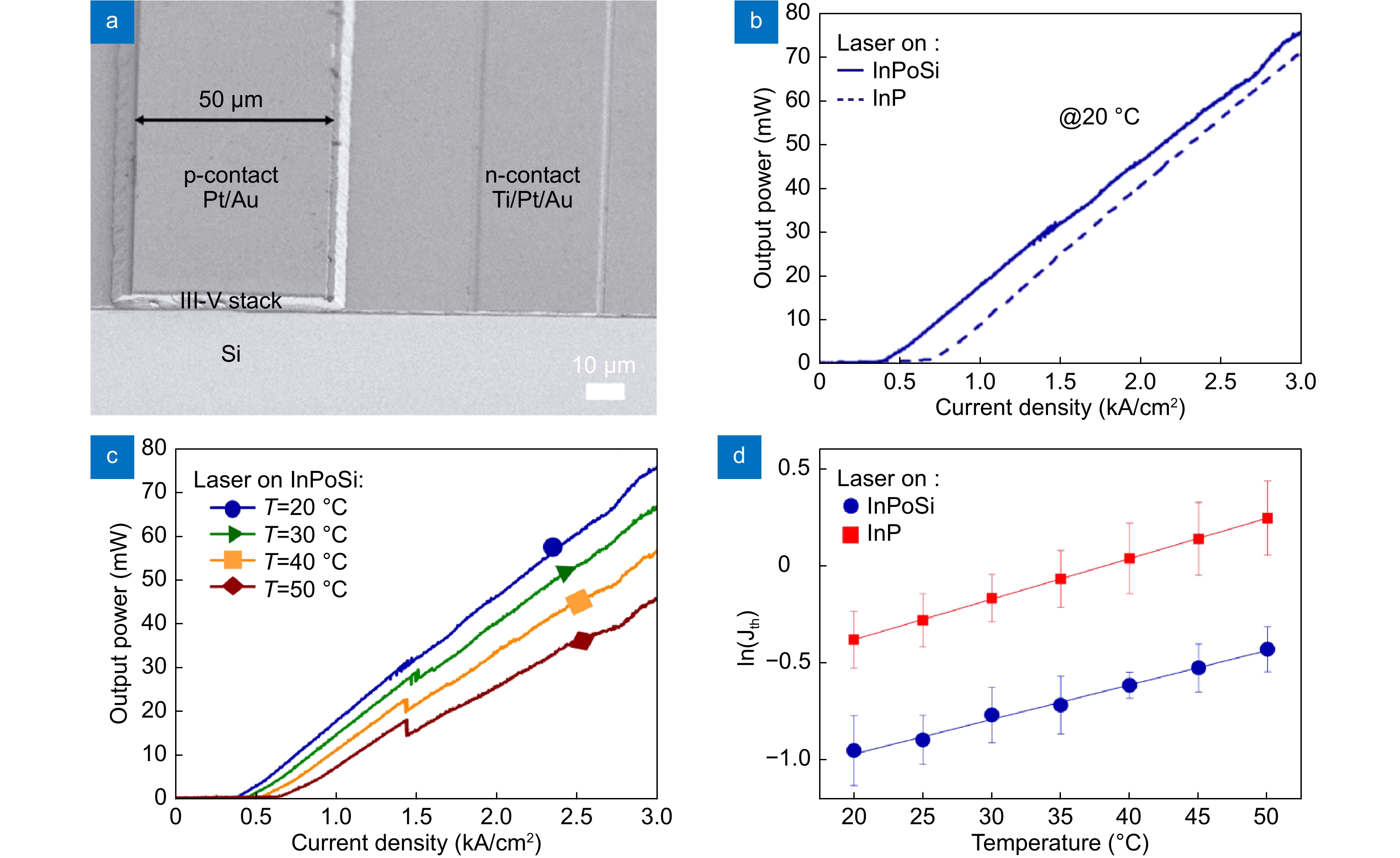
(a) SEM image of the fabricated FP laser on InP-on-Si substrate. (b) J-L characteristics in pulse injection mode at 20 °C: laser on bonded substrate (solid line) and the laser on InP (dash line). (c) J-L characteristics in pulse injection mode measured at different temperatures for the laser on bonded substrate. (d) Threshold current density evolution against temperature for the laser on bonded substrate (blue) and on InP (red). Figure repoduced with permisson from ref.32, IEEE.
-
Figure 12.
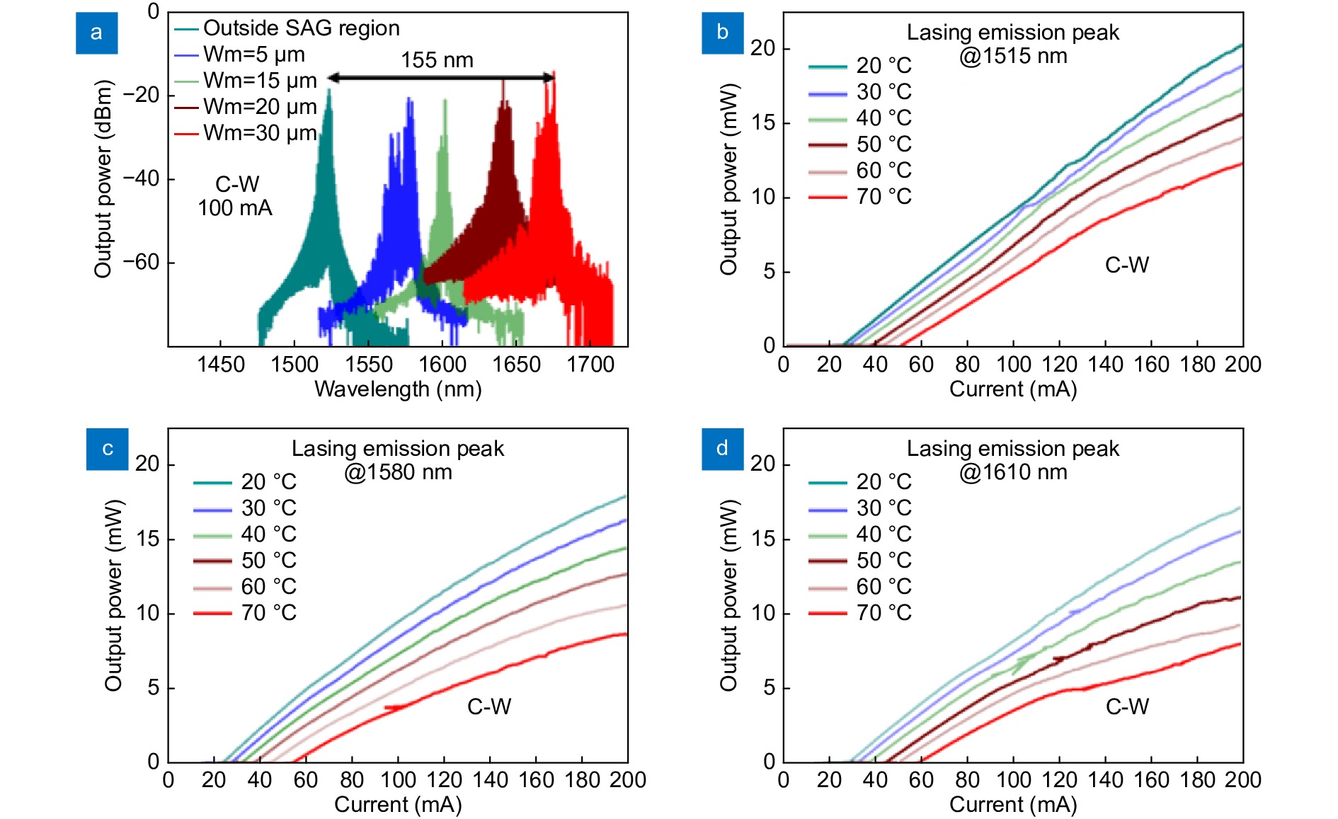
(a) Measured lasing spectra of five FP lasers under C-W operation for a driving current of 100 mA at 20 °C. (b−d) L-I characteristics under C-W operation for different temperatures for the lasers emitting at 1515 nm, 1580 nm and 1635 nm. Figure repoduced with permisson from ref.35, IEEE.
-
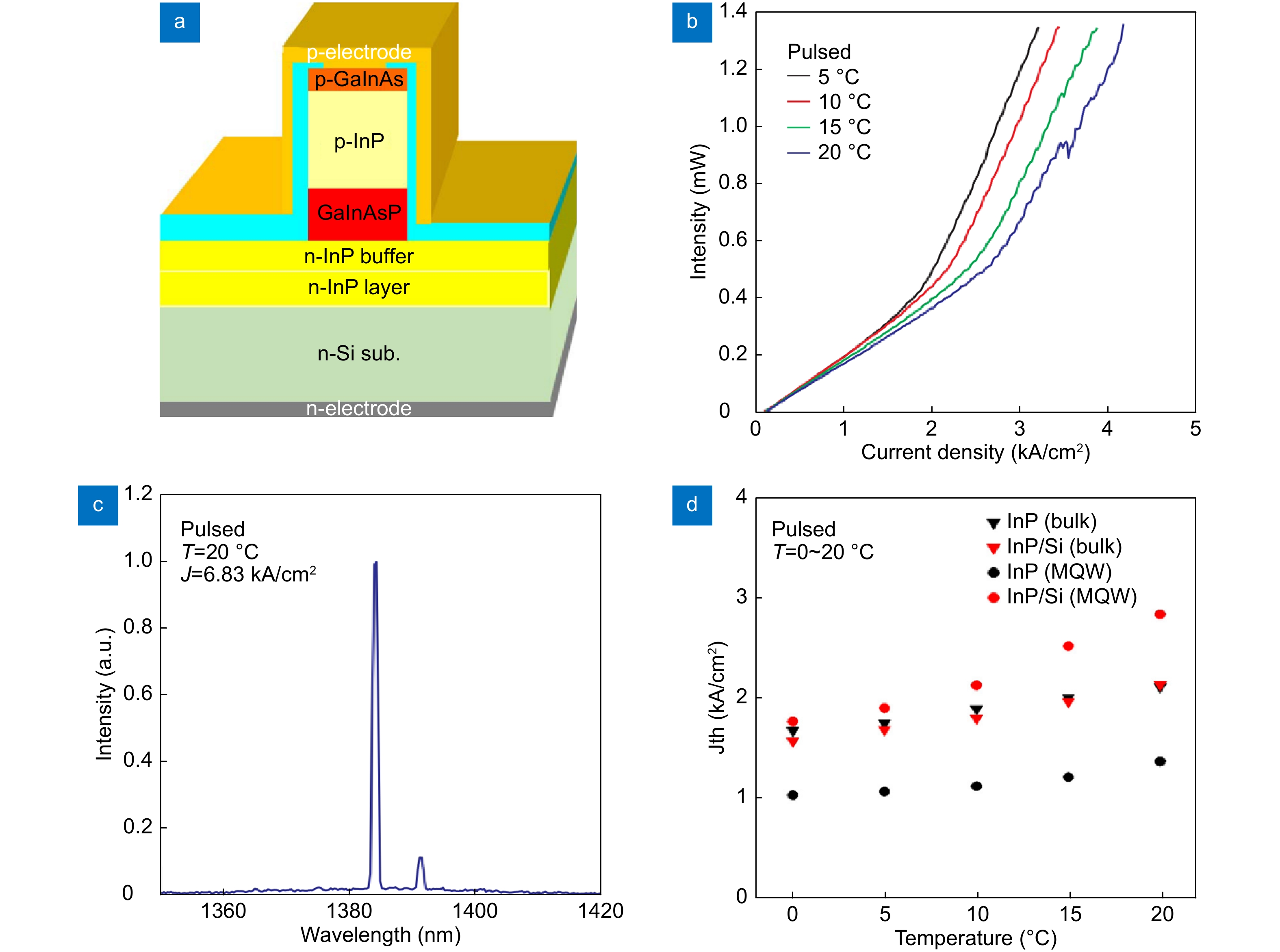
Figure 13.
(a) A typical laser structure. (b) The typical I-L characteristics of the MQW laser on the bonded substrate at various temperatures. (c) A lasing spectrum for the MQW laser at an input current of J=6.83 kA/cm2. (d) The temperature dependence of the threshold current density for the DH bulk lasers and MQW lasers on bonded substrates and on native substraes. Figure repoduced with permisson from: (a) ref.26, IEEE; (b, c, d) ref.27, Elsevier.


