
 E-mail Alert
 RSS
RSS
| Citation: |

|
Ultra-high extinction-ratio light modulation by electrically tunable metasurface using dual epsilon-near-zero resonances
-
Abstract
The lossy nature of indium tin oxide (ITO) at epsilon-near-zero (ENZ) wavelength is used to design an electrically tunable metasurface absorber. The metasurface unit cell is constructed of a circular resonator comprising two ITO discs and a high dielectric constant perovskite barium strontium titanate (BST) film. The ENZ wavelength in the accumulation and depletion layers of ITO discs is controlled by applying a single bias voltage. The coupling of magnetic dipole resonance with the ENZ wavelength inside the accumulation layer of ITO film causes total absorption of reflected light. The reflection amplitude can achieve ~84 dB or ~99.99% modulation depth in the operation wavelength of 820 nm at a bias voltage of −2.5 V. Moreover, the metasurface is insensitive to the polarization of the incident light due to the circular design of resonators and the symmetrical design of bias connections. -

-
References
[1] Holloway CL, Kuester EF, Gordon JA, O'Hara J, Booth J et al. An overview of the theory and applications of metasurfaces: the two-dimensional equivalents of metamaterials. IEEE Antenn Propag Mag 54, 10–35 (2012). [2] Yu NF, Capasso F. Flat optics with designer metasurfaces. Nat Mater 13, 139–150 (2014). doi: 10.1038/nmat3839 [3] Kildishev AV, Boltasseva A, Shalaev VM. Planar photonics with metasurfaces. Science 339, 1232009 (2013). doi: 10.1126/science.1232009 [4] Zhang YB, Liu H, Cheng H, Tian JG, and Chen SQ. Multidimensional manipulation of wave fields based on artificial microstructures. Opto-Electron Adv 3, 200002 (2020). doi: 10.29026/oea.2020.200002 [5] Ni XJ, Kildishev AV, Shalaev VM. Metasurface holograms for visible light. Nat Commun 4, 2807 (2013). doi: 10.1038/ncomms3807 [6] Khorasaninejad M, Chen WT, Devlin RC, Oh J, Zhu AY et al. Metalenses at visible wavelengths: Diffraction-limited focusing and subwavelength resolution imaging. Science 352, 1190–1194 (2016). doi: 10.1126/science.aaf6644 [7] Ma XL, Pu MB, Li X, Guo YH, Luo XG. All-metallic wide-angle metasurfaces for multifunctional polarization manipulation. Opto-Electron Adv 2 , 180023 (2019). doi: 10.29026/oea.2019.180023 [8] Glybovski SB, Tretyakov SA, Belov PA, Kivshar YS, Simovski CR. Metasurfaces: from microwaves to visible. Phys Rep 634, 1–72 (2016). doi: 10.1016/j.physrep.2016.04.004 [9] Nemati A, Wang Q, Hong MH, Teng JH. Tunable and reconfigurable metasurfaces and metadevices. Opto-Electron Adv 1, 180009 (2018). [10] Brar VW, Jang MS, Sherrott M, Lopez JJ, Atwater HA. Highly confined tunable mid-infrared plasmonics in graphene nanoresonators. Nano Lett 13, 2541–2547 (2013). doi: 10.1021/nl400601c [11] Sherrott MC, Hon PWC, Fountaine KT, Garcia JC, Ponti SM et al. Experimental demonstration of > 230° phase modulation in gate-tunable graphene–gold reconfigurable mid-infrared metasurfaces. Nano Lett 17, 3027–3034 (2017). doi: 10.1021/acs.nanolett.7b00359 [12] Ooi KJA, Leong PC, Ang LK, Tan DTH. All-optical control on a graphene-on-silicon waveguide modulator. Sci Rep 7, 12748 (2017). doi: 10.1038/s41598-017-13213-6 [13] Guo JY, Wang T, Quan BG, Zhao H, Gu CZ et al. Polarization multiplexing for double images display. Opto-Electron Adv 2 , 180029 (2019). doi: 10.29026/oea.2019.180029 [14] Dou KH, Xie X, Pu MB, Li X, Ma XL et al. Off-axis multi-wavelength dispersion controlling metalens for multi-color imaging. Opto-Electron Adv 3 , 190005 (2020). doi: 10.29026/oea.2020.190005 [15] Gao JW, Kempa K, Giersig M, Akinoglu EM, Han B et al. Physics of transparent conductors. Adv Phys 65, 553–617 (2016). doi: 10.1080/00018732.2016.1226804 [16] Chopra KL, Major S, Pandya DK. Transparent conductors—a status review. Thin Solid Films 102, 1–46 (1983). doi: 10.1016/0040-6090(83)90256-0 [17] Babicheva VE, Boltasseva A, Lavrinenko AV. Transparent conducting oxides for electro-optical plasmonic modulators. Nanophotonics 4, 165–185 (2015). doi: 10.1515/nanoph-2015-0004 [18] Ou JY, Plum E, Zhang JF, Zheludev NI. An electromechanically reconfigurable plasmonic metamaterial operating in the near-infrared. Nat Nanotechnol 8, 252–255 (2013). doi: 10.1038/nnano.2013.25 [19] Ee HS, Agarwal R. Tunable metasurface and flat optical zoom lens on a stretchable substrate. Nano Lett 16, 2818–2823 (2016). doi: 10.1021/acs.nanolett.6b00618 [20] Liu L, Kang L, Mayer TS, Werner DH. Hybrid metamaterials for electrically triggered multifunctional control. Nat Commun 7, 13236 (2016). doi: 10.1038/ncomms13236 [21] ForouzmA, Salary MM, Inampudi S, Mosallaei H. A tunable multigate Indium‐Tin‐oxide‐assisted all‐dielectric metasurface. Adv Opt Mater 6, 1701275 (2018). doi: 10.1002/adom.201701275 [22] Kafaie Shirmanesh G, Sokhoyan R, Pala RA, Atwater HA. Dual-gated active metasurface at 1550 nm with wide (> 300°) phase tunability. Nano Lett 18, 2957–2963 (2018). doi: 10.1021/acs.nanolett.8b00351 [23] Huang YW, Lee HW, Sokhoyan R, Pala RA, Thyagarajan K et al. Gate-tunable conducting oxide metasurfaces. Nano Lett 16, 5319–5325 (2016). doi: 10.1021/acs.nanolett.6b00555 [24] Park J, Jeong BG, Kim SI, Lee D, Kim J et al. All-solid-state spatial light modulator with independent phase and amplitude control for three-dimensional LiDAR applications. Nat Nanotechnol 16, 69–76 (2021). doi: 10.1038/s41565-020-00787-y [25] Park J, Kang JH, Liu XG, Brongersma ML. Electrically tunable epsilon-near-zero (ENZ) metafilm absorbers. Sci Rep 5, 15754 (2015). doi: 10.1038/srep15754 [26] Shi KF, Haque RR, Zhao BY, Zhao RC, Lu ZL. Broadband electro-optical modulator based on transparent conducting oxide. Opt Lett 39, 4978–4981 (2014). doi: 10.1364/OL.39.004978 [27] Lee Y, Yun J, Kim SJ, Seo M, In S et al. High‐speed transmission control in gate‐tunable metasurfaces using hybrid plasmonic waveguide mode. Adv Opt Mater 8, 2001256 (2020). doi: 10.1002/adom.202001256 [28] Howes A, Wang WY, Kravchenko I, Valentine J. Dynamic transmission control based on all-dielectric Huygens metasurfaces. Optica 5, 787–792 (2018). doi: 10.1364/OPTICA.5.000787 [29] Nemati A, Qian W, Hong MH, Teng JH. Electrically tunable polarization-insensitive MIM plasmonic metasurface operating in transmission mode. J Opt 21, 055102 (2019). doi: 10.1088/2040-8986/ab1383 [30] Edwards PP, Porch A, Jones MO, Morgan DV, Perks RM. Basic materials physics of transparent conducting oxides. Dalton Trans 19, 2995–3002 (2004). doi: 10.1039/B408864F [31] Alù A, Silveirinha MG, Salandrino A, Engheta N. Epsilon-near-zero metamaterials and electromagnetic sources: Tailoring the radiation phase pattern. Phys Rev B 75, 155410 (2007). doi: 10.1103/PhysRevB.75.155410 [32] Liberal I, Engheta N. The rise of near-zero-index technologies. Science 358, 1540–1541 (2017). doi: 10.1126/science.aaq0459 [33] Naik GV, Kim J, Boltasseva A. Oxides and nitrides as alternative plasmonic materials in the optical range[Invited]. Opt Mater Express 1, 1090–1099 (2011). doi: 10.1364/OME.1.001090 [34] Kinsey N, DeVault C, Boltasseva A, Shalaev VM. Near-zero-index materials for photonics. Nat Rev Mater 4, 742–760 (2019). doi: 10.1038/s41578-019-0133-0 [35] Lobet M, Liberal I, Knall EN, Alam MZ, Reshef O et al. Fundamental radiative processes in near-zero-index media of various dimensionalities. ACS Photonics 7, 1965–1970 (2020). doi: 10.1021/acsphotonics.0c00782 [36] Chen AQ, Zhu KG, Zhong HC, Shao QY, Ge GL. A new investigation of oxygen flow influence on ITO thin films by magnetron sputtering. Solar Energy Mater Solar Cells 120, 157–162 (2014). doi: 10.1016/j.solmat.2013.08.036 [37] Izumi H, Adurodija FO, Kaneyoshi T, Ishihara T, Yoshioka H et al. Electrical and structural properties of indium tin oxide films prepared by pulsed laser deposition. J Appl Phys 91, 1213–1218 (2002). doi: 10.1063/1.1427137 [38] Gorzkowski EP, Pan MJ, Bender B, Wu CCM. Glass-ceramics of barium strontium titanate for high energy density capacitors. J Electroceram 18, 269–276 (2007). doi: 10.1007/s10832-007-9127-1 [39] Vidhya VS, Malathy V, Balasubramanian T, Saaminathan V, Sanjeeviraja C et al. Influence of RF power on the growth mechanism, preferential orientation and optoelectronic properties of nanocrystalline ITO films. Curr Appl Phys 11, 286–294 (2011). doi: 10.1016/j.cap.2010.07.021 [40] Fan JCC, Goodenough JB. X‐ray photoemission spectroscopy studies of Sn‐doped indium‐oxide films. J Appl Phys 48, 3524–3531 (1977). doi: 10.1063/1.324149 [41] Forouzmand A, Salary MM, Shirmanesh GK, Sokhoyan R, Atwater HA et al. Tunable all-dielectric metasurface for phase modulation of the reflected and transmitted light via permittivity tuning of indium tin oxide. Nanophotonics 8, 415–427 (2019). doi: 10.1515/nanoph-2018-0176 [42] Silveirinha MG, Engheta N. Theory of supercoupling, squeezing wave energy, and field confinement in narrow channels and tight bends using ε near-zero metamaterials. Phys Rev B 76, 245109 (2007). doi: 10.1103/PhysRevB.76.245109 -
Supplementary Information
Supplementary information for Ultra-high extinction-ratio light modulation by electrically tunable metasurface using dual epsilon-near-zero resonances 
-
Access History

Figures(8)
Tables(1)
Article Metrics

Export File
Citation
Format
Content
 DownLoad:


-
Figure 1.
Schematic of the tunable double ITO capacitive structure.
-
Figure 2.
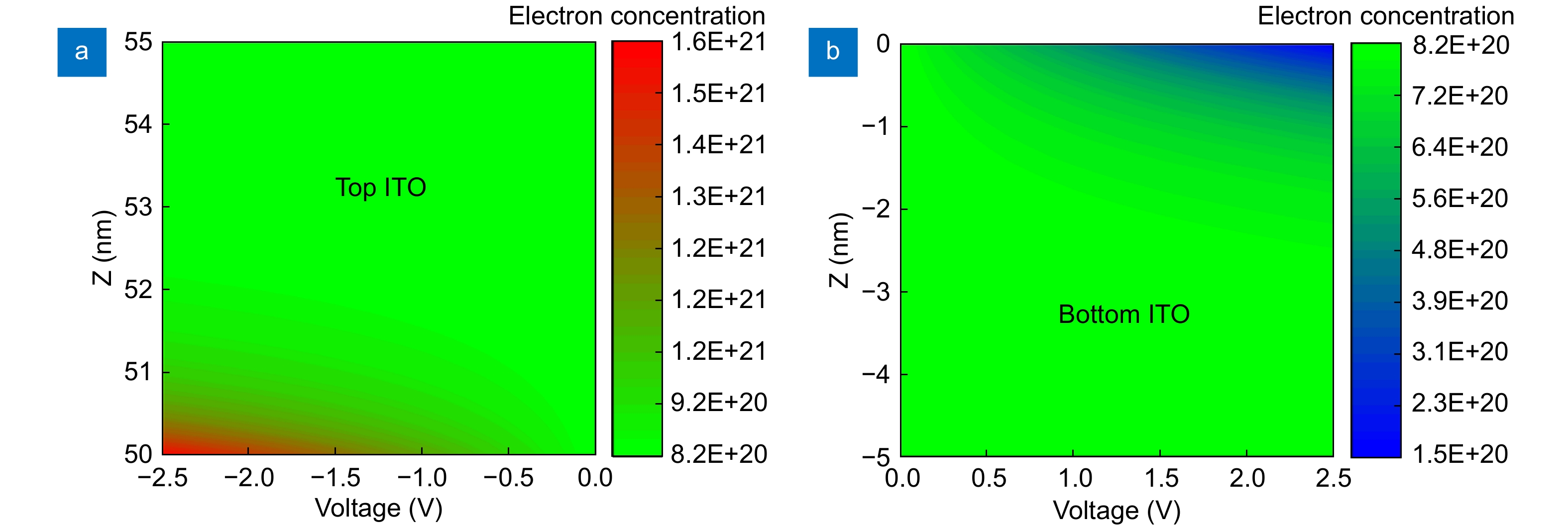
Electron concentrations in the (a) top and (b) bottom ITO films as functions of the applied voltage. The electron concentration along the Z axis, 50 nm < Z < 55 nm in the top ITO film and −5 nm < Z < 0 nm in the bottom ITO film. The initial electron concentration for both films equal to N0 = 8.22 × 1020 cm−3 is shown in green color. The increased electron concentration is shown with red color in the accumulation layer of the top ITO film and the decreased electron concentration is shown with blue color in the depletion layer of the bottom ITO film.
-
Figure 3.
Optical properties of ITO film as functions of the applied voltage. The optical properties of the ITO film interface with the BST film in three different conditions. Na represents the optical property of the accumulation layer, Nd represents the optical property of the depletion layer, and N0 represents the optical property of interface without bias voltage (un-biased) and all other parts of the ITO film. (a) The real part of the permittivity
${{ \text{ε}_{{\rm{r}}}'\left(\omega \right)}}$ ${{ \text{ε}}_{{\rm{r}}}}''\left(\omega \right)$ -
Figure 4.
Schematic of the electrically controlled reflective modulator metasurface. (a) A square unit cell is constructed from a circular silicon resonator on the top of a circular ITO-BST-ITO resonator on the top of a silver mirror. Four symmetrical bias connections with the same layers are used to make bias connections between the ITO films. Parameter values are tAg =100 nm, tITO = 5 nm, tBST = 50 nm, tSi = 50 nm, W = 20 nm, D = 250 nm, and P = 520 nm. The initial polarization of light is shown along the X axis. (b) 3D schematic of the metasurface constructed from a 6×6 array of unit cells. The metasurface is controlled by applying the voltage between the bottom silver film (grey) and the top ITO electrode (orange). The electrical current passes to the resonators through a 2D array of bias connections.
-
Figure 5.
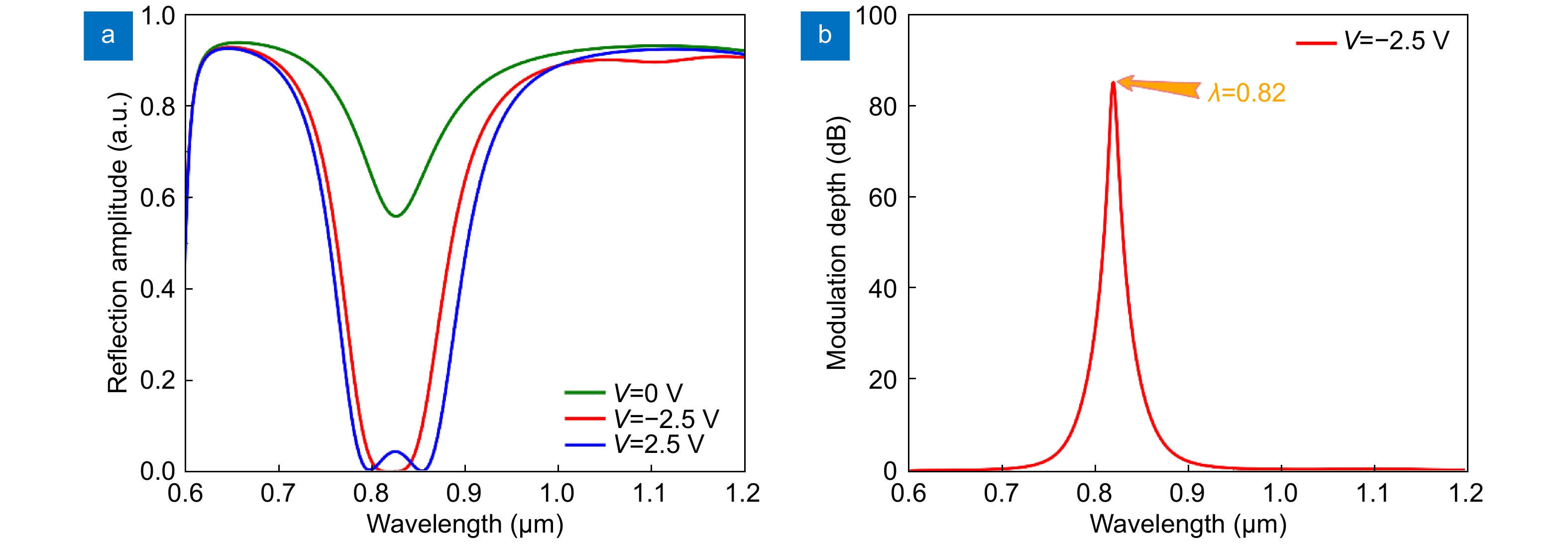
Performance of the electrically tunable modulator metasurface. (a) Simulated reflection spectra of the modulator under three different voltages. Under V = 0 V bias voltage, both ITO films have an electron concentration of N0. Under V = −2.5 V, the top ITO film has a 0.5 nm thick accumulation layer with an electron concentration of Na and the bottom ITO film has a 1 nm thick depletion layer with an electron concentration of Nd. Under V = 2.5 V, the top ITO film has a depletion layer with an electron concentration of Nd and the bottom ITO film has an accumulation layer with an electron concentration of Na. (b) Modulation depth spectra of modulator under V = −2.5 V. The modulation depth peaks to ~84 dB at the wavelength of λ = 820 nm.
-
Figure 6.
Electric field intensity along XZ plane under the bias voltages of (a) V = 0 V at λ = 820 nm, (b) V = 2.5 V at λ = 800 nm, and (c) V = −2.5 V at λ = 820 nm. The edges of the Si disc and silver mirror are shown with green dashed lines.
-
Figure 7.
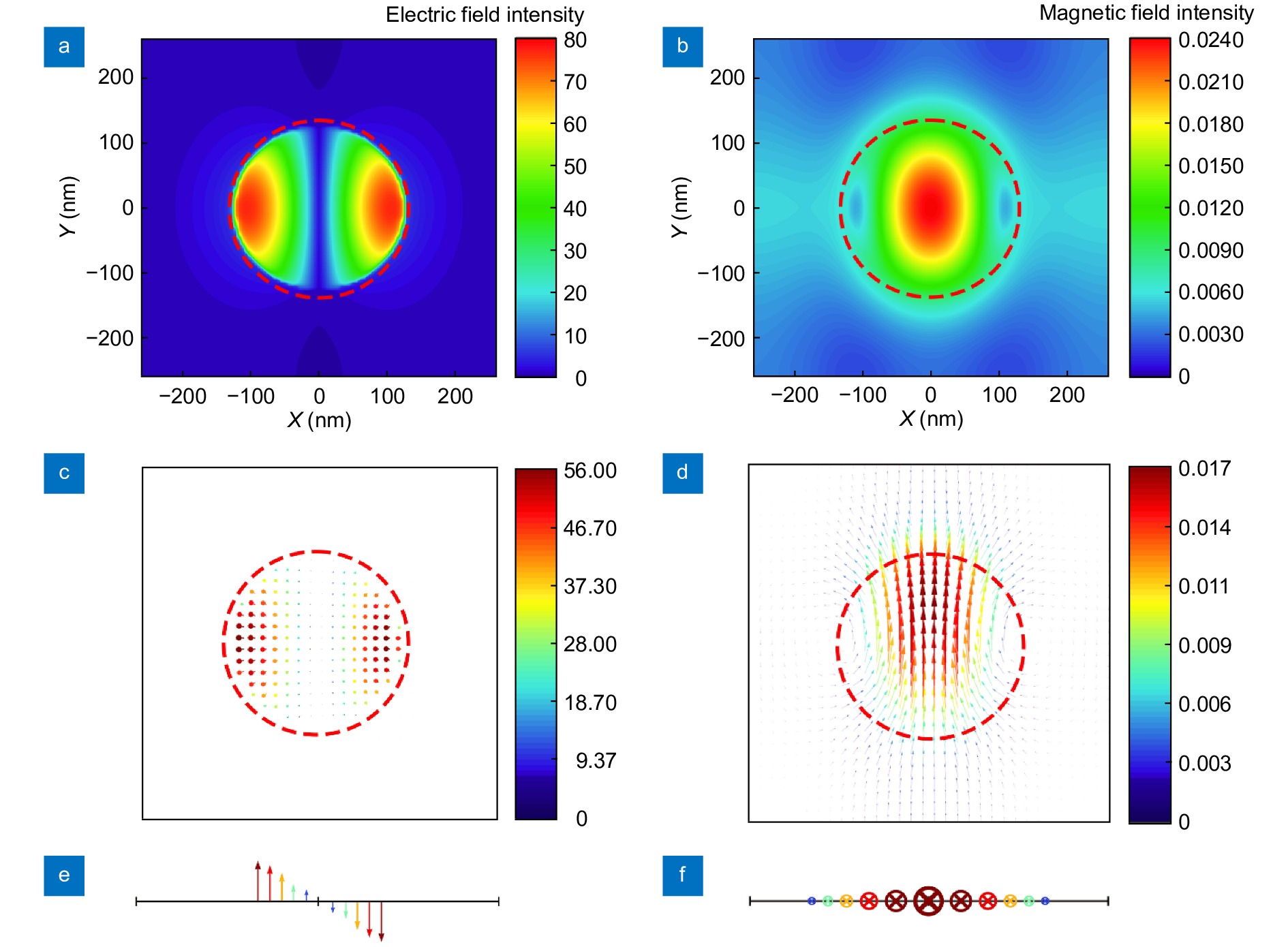
The electric and magnetic fields under a bias voltage of V = −2.5 V inside the accumulation layer at λ = 820 nm. (a) Electric and (b) magnetic field intensities in the XY plane inside the accumulation layer in the top ITO film. Top view of the vectors of the (c) electric and (d) magnetic fields from the same monitor. Side view of the vectors of the (e) electric and (f) magnetic fields from the same monitor. The vector figures (e) and (f) share the same scalar bar as vector figures (c) and (d), respectively. The edge of the ITO disc is shown by the red dashed lines.
-
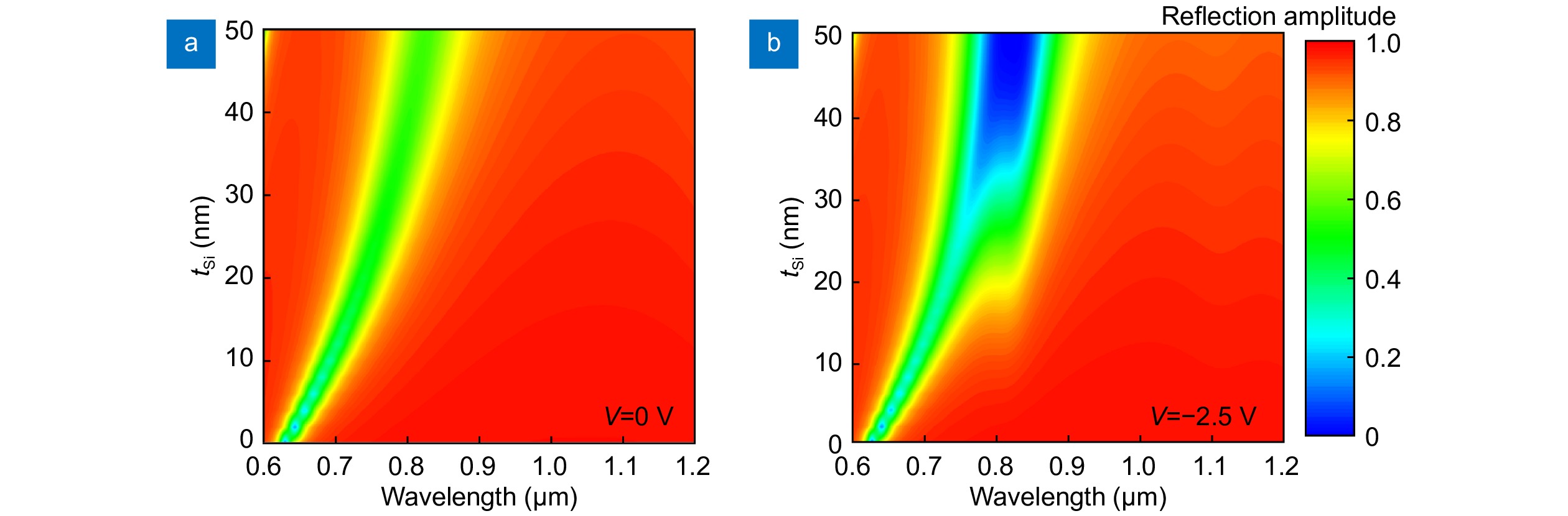
Figure 8.
Impact of the Si disc thickness on the reflection spectra. Map of the reflection spectra of the modulator metasurface with a varying thickness of the Si disc (0 nm ≤ tSi ≤ 50 nm) under the bias voltages of (a) V = 0 V and (b) V = −2.5 V.


