
 E-mail Alert
 RSS
RSS
| Citation: |

|
Achromatic metalens based on coordinative modulation of propagation phase and geometric phase
-
Abstract
Metalens is considered as one of the most promising planar optical devices composed of the metasurface, but it is usually difficult to realize full-color imaging and display due to the narrow working bandwidth and large chromatic aberration. In this paper, a phase-controlled transmissive metalens is designed to realize the broadband achromatic focusing within 400 nm~650 nm, and the average focusing efficiency is about 29% at the focal plane within the bandwidth range. The titanium dioxide (TiO2) dielectric nanopillar with low loss and high refractive index as a truncated waveguide can control the propagation phase in the visible. At the same time, we analyze the dispersion modulation mechanism which merges the geometric and propagation phases, and the particle swarm optimization (PSO) algorithm is used to optimize the phase response database, and accomplish the phase matching between the ideal and actual wavefronts. The proposed broadband achromatic devices may broaden the applications of metalens in micro-imaging, computer vision, and machine vision.-
Keywords:
- metalens /
- visible /
- achromatic /
- broadband
-

-
References
[1] Luo X G. Principles of electromagnetic waves in metasurfaces[J]. Science China Physics, Mechanics & Astronomy, 2015, 58(9): 594201. [2] 蒲明博, 王长涛, 王彦钦, 等.衍射极限尺度下的亚波长电磁学[J].物理学报, 2017, 66(14): 144101. Pu M B, Wang C T, Wang Y Q, et al. Subwavelength electromagnetics below the diffraction limit[J]. Acta Physica Sinica, 2017, 66(14): 144101. [3] Wu P C, Zhu W M, Shen Z X, et al. Broadband wide-angle multifunctional polarization converter via liquid-metal-based metasurface[J]. Advanced Optical Materials, 2017, 5(7): 1600938. doi: 10.1002/adom.201600938 [4] Pu M B, Li X, Ma X L, et al. Catenary optics for achromatic generation of perfect optical angular momentum[J]. Science Advances, 2015, 1(9): e1500396. doi: 10.1126/sciadv.1500396 [5] Yue F Y, Wen D D, Xin J T, et al. Vector vortex beam generation with a single plasmonic metasurface[J]. ACS Photonics, 2016, 3(9): 1558-1563. doi: 10.1021/acsphotonics.6b00392 [6] Wang S C, Ouyang X Y, Feng Z W, et al. Diffractive photonic applications mediated by laser reduced graphene oxides[J]. Opto-Electronic Advances, 2018, 1(2): 170002. doi: 10.29026/oea.2018.170002 [7] Li Z, Cheng H, Liu Z C, et al. Plasmonic airy beam generation by both phase and amplitude modulation with metasurfaces[J]. Advanced Optical Materials, 2016, 4(8): 1230-1235. doi: 10.1002/adom.201600108 [8] 陈俊妍, 张飞, 张明, 等.基于介质超表面的径向偏振贝塞尔透镜[J].光电工程, 2018, 45(11): 180124. doi: 10.12086/oee.2018.180124 Chen J Y, Zhang F, Zhang M, et al. Radially polarized bessel lens based on all-dielectric metasurface[J]. Opto-Electronic Engineering, 2018, 45(11): 180124. doi: 10.12086/oee.2018.180124 [9] Huang L L, Mühlenbernd H, Li X W, et al. Broadband hybrid holographic multiplexing with geometric metasurfaces[J]. Advanced Materials, 2015, 27(41): 6444-6449. doi: 10.1002/adma.201502541 [10] Huang Y W, Chen W T, Tsai W Y, et al. Aluminum plasmonic multicolor meta-hologram[J]. Nano Letters, 2015, 15(5): 3122-3127. doi: 10.1021/acs.nanolett.5b00184 [11] Ni X J, Kildishev A V, Shalaev V M. Metasurface holograms for visible light[J]. Nature Communications, 2013, 4(1): 2807. doi: 10.1038/ncomms3807 [12] Wan W W, Gao J, Yang X D. Full-color plasmonic metasurface holograms[J]. ACS Nano, 2016, 10(12): 10671-10680. doi: 10.1021/acsnano.6b05453 [13] Ni X J, Wong Z J, Mrejen M, et al. An ultrathin invisibility skin cloak for visible light[J]. Science, 2015, 349(6254): 1310-1314. doi: 10.1126/science.aac9411 [14] Xie X, Pu M B, Li X, et al. Dual-band and ultra-broadband photonic spin-orbit interaction for electromagnetic shaping based on single-layer silicon metasurfaces[J]. Photonics Research, 2019, 7(5): 586-593. doi: 10.1364/PRJ.7.000586 [15] Dou K H, Xin X, Pu M B, et al. Off-axis multi-wavelength dispersion controlling metalens for multi-color imaging[J]. Opto-Electronic Advances, 2020, 3(4): 190005. doi: 10.29026/oea.2020.190005 [16] Shrestha S, Overvig A C, Lu M, et al. Broadband achromatic dielectric metalenses[J]. Light: Science & Applications, 2018, 7: 85. [17] Li Y, Li X, Pu M B, et al. Achromatic flat optical components via compensation between structure and material dispersions[J]. Scientific Reports, 2016, 6(1): 19885. doi: 10.1038/srep19885 [18] Yan C, Li X, Pu M B, et al. Midinfrared real-time polarization imaging with all-dielectric metasurfaces[J]. Applied Physics Letters, 2019, 114(16): 161904. doi: 10.1063/1.5091475 [19] Khorasaninejad M, Aieta F, Kanhaiya P, et al. Achromatic metasurface lens at telecommunication wavelengths[J]. Nano Letters, 2015, 15(8): 5358-5362. doi: 10.1021/acs.nanolett.5b01727 [20] Shi Z J, Khorasaninejad M, Huang Y W, et al. Single-layer metasurface with controllable multiwavelength functions[J]. Nano Letters, 2018, 18(4): 2420-2427. doi: 10.1021/acs.nanolett.7b05458 [21] Groever B, Chen W T, Capasso F. Meta-lens doublet in the visible region[J]. Nano Letters, 2017, 17(8): 4902-4907. doi: 10.1021/acs.nanolett.7b01888 [22] Khorasaninejad M, Shi Z, Zhu A Y, et al. Achromatic metalens over 60 nm bandwidth in the visible and metalens with reverse chromatic dispersion[J]. Nano Letters, 2017, 17(3): 1819-1824. [23] Chen W T, Zhu A Y, Sanjeev V, et al. A broadband achromatic metalens for focusing and imaging in the visible[J]. Nature Nanotechnology, 2018, 13(3): 220-226. doi: 10.1038/s41565-017-0034-6 [24] Wang S M, Wu P C, Su V C, et al. A broadband achromatic metalens in the visible[J]. Nature Nanotechnology, 2018, 13(3): 227-232. doi: 10.1038/s41565-017-0052-4 [25] Wang S M, Wu P C, Su V C, et al. Broadband achromatic optical metasurface devices[J]. Nature Communications, 2017, 8(1): 187. doi: 10.1038/s41467-017-00166-7 [26] Pancharatnam S. Generalized theory of interference and its applications[J]. Proceedings of the Indian Academy of Sciences-Section A, 1956, 44(6): 398-417. doi: 10.1007/BF03046095 [27] Berry M V. Quantal phase factors accompanying adiabatic changes[J]. Proceedings of the Royal Society of London A Mathematical, and Physical Sciences, 1984, 392(1802): 45-57. doi: 10.1098/rspa.1984.0023 [28] Zhang F, Pu M B, Li X, et al. All-dielectric metasurfaces for simultaneous giant circular asymmetric transmission and wavefront shaping based on asymmetric photonic spin-orbit Interactions[J]. Advanced Functional Materials, 2017, 27(47): 1704295. doi: 10.1002/adfm.201704295 [29] Devlin R C, Khorasaninejad M, Chen W T, et al. High efficiency dielectric metasurfaces at visible wavelengths[Z]. arXiv 1603.02735[physics.optics], 2016. [30] Khorasaninejad M, Chen W T, Devlin R C, et al. Planar Lenses at Visible Wavelengths[Z]. arXiv 1605.02248[physics.optics], 2016. [31] Kennedy J, Eberhart R. Particle swarm optimization[C]//Proceedings of ICNN'95-International Conference on Neural Networks, Perth, 1995, 4: 1942-1948. [32] Barakat R. Rayleigh wavefront criterion[J]. Josa, 1965, 55(5): 572-573. doi: 10.1364/JOSA.55.000572 -
Overview

Overview: As a two-dimension artificial electromagnetic material, metasurface provides the means to accurately control the wavefront by flexibly adjusting the phase, amplitude, and polarization of electromagnetic waves at will. At present, many applications based on metasurface have been proved, such as beam generator, optical holographic imaging, virtual shaping, and so on. As a plane lens, the metasurface can also generate a hyperbolic phase profile to obtain a focused beam with a higher diffraction efficiency. Traditional refractive lenses achieve phase accumulation by changing the thickness of optical materials, which is usually curved. In contrast, the metalens can realize phase modulation of electromagnetic waves in a plane manner. However, it is usually difficult to realize full-color imaging and display due to the narrow working bandwidth and large chromatic aberration which are caused by the intrinsic properties of the material. In this paper, a phase-controlled transmissive metalens is designed, to realize the broadband achromatic focusing within 400 nm~650 nm, and the average focusing efficiency is about 29% at the focal plane within the bandwidth range. The metalens is composed of titanium dioxide (TiO2) dielectric nanopillars arranged periodically on a silicon dioxide (SiO2, n=1.45) substrate. The nanopillar possesses low loss and high refractive index which can be treated as a truncated waveguide to control the propagation phase in the visible. At the same time, we analyze the dispersion modulation mechanism which merges the geometric and propagation phases, and the particle swarm optimization (PSO) algorithm is used to optimize the phase response database, and accomplish the phase matching between the ideal focusing and the actual wavefronts and realize the designed function. The proposed broadband achromatic planar optical device has a simple structure design of unit cell, therefore we can introduce more types of resonance units to realize the achromatic focusing function with a larger bandwidth.
-
Access History


Export File
Citation
Format
Content
 DownLoad:
-
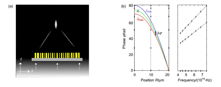
Figure 1.
A broadband achromatic metalens. (a) The focal length will always remain unchanged while the incident wavelength varies from 400 nm to 650 nm, and the incident beam will converge into a white focus; (b) The phase profile for a broadband achromatic metalens at arbitrary wavelength of λ∈(λmin, λmax), and the right illustration shows the required phase for different wavelengths at different positions
-
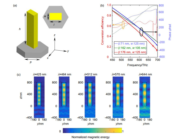
Figure 2.
The simulation results of unit-cell. (a) The unit cell of a broadband achromatic metalens in the visible light region; (b) Conversion efficiency (dotted line) and phase profile with varying slope (solid line) for different structure parameter combination (l: 71 nm, w: 125 nm、l: 162 nm, w: 105 nm、l: 176 nm, w: 125 nm); (c) Under different incident wavelengths, the normalized magnetic energy distribution is obtained when the structure parameter is l=105 nm and w=80 nm. The black line indicates the boundary of the TiO2 structure
-
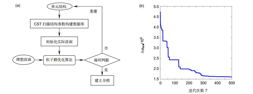
Figure 3.
(a) Flow chart of the PSO for broadband achromatic metalens; (b) The convergence curve of PSO
-
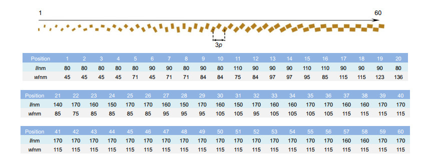
Figure 4.
Those structure parameters of the radial unit cells for metalens
-
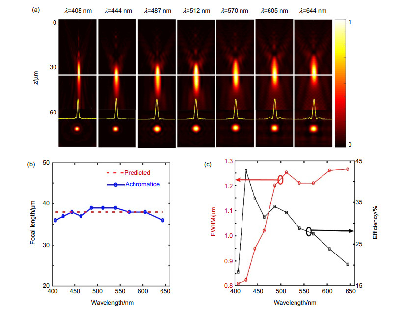
Figure 5.
Simulated results of the focal length shifts and intensity distributions of metalens. (a) The normalized intensity distribution in the y-z plane and focused spot in the x-y plane at normal incidence. The direction of incidence is towards the positive z-axis. The white dashed line represents theoretical focal length f=38 μm and the yellow dotted lines indicate point spread function; (b) The simulated focal length and the theoretically predicted focal length as a function of the wavelength; (c) Focusing efficiency and FWHM as the changes of incident wavelengths obtained from the broadband achromatic metalens


