
 E-mail Alert
 RSS
RSS
-
摘要:
本文总结了当前同步辐射X射线反射镜光学制造技术的需求背景、发展现状以及未来方向。同步辐射光源是国家重大科学装置,作为同步辐射光源重要光学元件的X射线反射镜,直接决定着光学调制品质。短波长掠入射的特殊应用场景,使X射线反射镜有着更为特殊且高精度的面形要求,其加工与检测技术长期为国外所垄断,国内发展较为缓慢,面对国内未来同步辐射装置的建设需求,我国亟需打破这一现状。
Abstract:This article reviews on the fabrication advancement of X-ray reflect mirror fabrication in terms of technical requirements, fabrication and metrology development. Synchrotron radiation source, as a revolutionary light source, provides one of the most high-performance X-ray for scientific research, where reflect mirror plays an essential role in X-ray beam focusing. The short wavelength of X-ray demands reflecting photons only at a grazing angle of incidence on the extremely high-precision and smooth surface. Fabrication of such mirrors requires highly specialized equipment and technology that only a few foreign optic manufacturers possess, whereas manufacturers in China is laggard in this area. It is imperative to develop fabrication capability domestically as two synchrotron radiation facilities are under construction and several more projects are about to launch in the near future in China.
-
Key words:
- X-ray focusing /
- synchrotron radiation light source /
- short wavelength /
- reflector
-

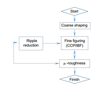
Overview: This article reviews on the fabrication technology of X-ray reflect mirror. Synchrotron radiation source, as a revolutionary light source, provides one of the most high-performance X-ray for scientific research, where reflect mirror plays an essential role in X-ray beam focusing. The short wavelength of X-ray requires reflecting photons only at a grazing angle of incidence on the extremely high-precision and smooth surface. Theoretically, a reflector only with the surface error no more than 1 nm (RMS) and slope error better than 50 nrad can meet the 4th generation synchrotron facility criterion, which is equivalent to controlling the surface height variance to as low as several-silicon-atom layers over hundreds-of-millimeter length. Relationship of the surface accuracy at each spatial frequency and mirror performance is explained in the article. These extreme demands make fabrication of such mirror depends highly upon specialized equipment and technology concerning both fabrication and metrology. Fabrication route can be sorted into two approaches. One is ion-beam-figuring-centered fabrication which realizes a slope error of 0.1 μrad~0.3 μrad (RMS) and roughness less than 0.3 nm (RMS) by means of IBF combined with ripple reduction and roughness improvement procedures, the latter of which are mainly deployed to ease the mid- and high-spatial-frequency surface errors brought by small tools polishing tracks. The other route is the elastic emission machining (EEM) method, which, along with plasma chemical vaporization machining (PVCM), is capable of producing state of the art X-ray focusing mirror over 1 m length with surface height error as low as 1 nm (P-V) and roughness lower than 0.1 nm (RMS). Surface height error at mid- and high- frequencies are diminished through gradual increase of polishing resolution. Surface metrology accuracy directly determines the limit of fabrication quality. Long trace profiler (LTP), a one dimensional figure measuring method, can perform extremely precise measurement especially on flat mirrors. It is essential and commonly used at light sources for mirror adjustment before mirrors being put in a beamline. Research on improving accuracy of LTP has been a shared effort of Metrology Labs at light sources. Ultrahigh-accuracy stitching interferometry is capable of providing two-dimensional surface map with higher lateral resolution, and is irreplaceable at fabrication sites for deterministic polishing process. To improve the stitching accuracy, means to determine geometric relationship of neighboring data has been developed, such as micro-stitching interferometry (MSI) and relative angle determinable stitching interferometry (RADSI) which is proven to give good performance. China is still at the early stage in this area which can hardly meet the need of the two under-construction synchrotron radiation facilities (HEPS and SHINE) and let alone several more projects about to launch in the near future in China. It is imperative to develop fabrication technique and capability domestically.
-

-
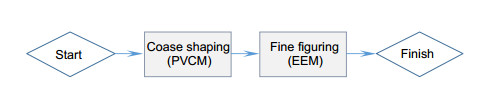
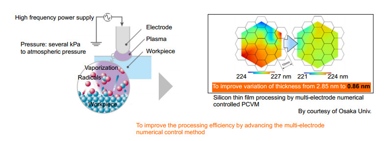
图 2 日本大阪大学X射线反射镜加工工艺路线
Figure 2. X-ray optic fabrication system developed by Osaka University
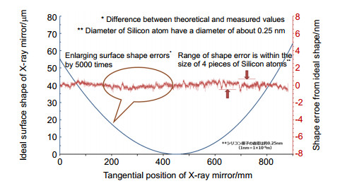
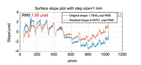
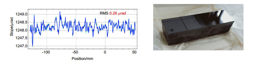
图 6 光电所1.26 m异形长条压弯镜面形斜率误差加工结果
Figure 6. Slope error of 1.26 meter long X-ray mirror provided by Institute of Optics and Electronics
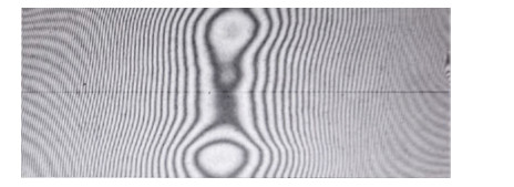
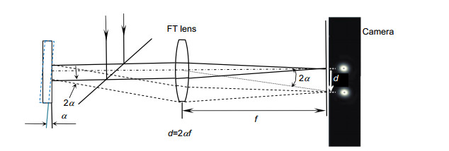
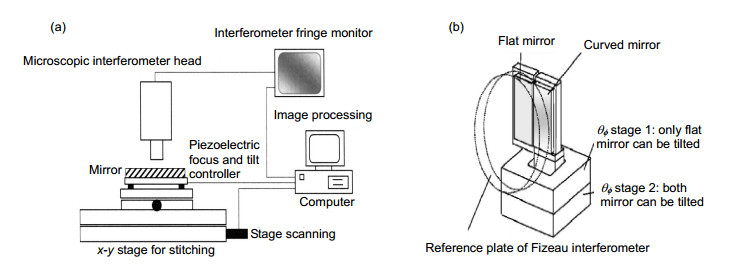
图 10 平面标准镜头检非球面度较大的元件干涉条纹图
Figure 10. Interference fringe image of the strong curved mirror measured by reference flat
-
[1] Codling K. Applications of synchrotron radiation (ultraviolet spectral light source)[J]. Reports on Progress in Physics, 1973, 36(5): 541-624. doi: 10.1088/0034-4885/36/5/002
[2] 姜晓明, 王九庆, 秦庆, 等.中国高能同步辐射光源及其验证装置工程[J].中国科学:物理学力学天文学, 2014, 44(10): 1075-1094. http://www.wanfangdata.com.cn/details/detail.do?_type=perio&id=zgkx-cg201410007
[3] Winick H. Synchrotron radiation sources - present capabilities and future directions[J]. Journal of Synchrotron Radiation, 1998, 5(3): 168-175. doi: 10.1107/S0909049597018761
[4] Susini J, Pauschinger D, Geyl R, et al. Hard x-ray mirror fabrication capabilities in Europe[J]. Optical Engineering, 1995, 34(2): 388-395. doi: 10.1117/12.194836
[5] Makeev M A, Cuerno R, Barabási A L. Morphology of ion-sputtered surfaces[J]. Nuclear Instruments and Methods in Physics Research Section B: Beam Interactions with Materials and Atoms, 2002, 197(3-4): 185-227. doi: 10.1016/S0168-583X(02)01436-2
[6] Schindler A, Haensel T, Flamm D, et al. Ion beam and plasma jet etching for optical component fabrication[J]. Proceedings of SPIE, 2001, 4440: 217-227. doi: 10.1117/12.448043
[7] Li A G, Takino H, Frost F. Ion beam planarization of diamond turned surfaces with various roughness profiles[J]. Optics Express, 2017, 25(7): 7828-7838. doi: 10.1364/OE.25.007828
[8] Zhou L, Li S Y, Liao W L, et al. Ion beam technology : figuring, smoothing and adding for high-precision optics[C]//Proceedings of Optical Fabrication and Testing 2014, Kohala Coast, Hawaii, 2014: 4-6.
[9] Mori Y, Yamauchi K, Hirose K, et al. Numerically controlled EEM (Elastic Emission Machining) system for ultraprecision figuring and smoothing of aspherical surfaces[M]//Scheel H J, Fukuda T. Crystal Growth Technology. Norwich: John Wiley & Sons, Ltd, 2013: 2.
[10] https://www.j-tec.co.jp/english/optical/high-precision-x-ray-mirror/.
[11] Mori Y, Yamauchi K, Yamamura K, et al. Development of plasma chemical vaporization machining[J]. Review of Scientific Instruments, 2000, 71(12): 4627-4632. doi: 10.1063/1.1322581
[12] Takino H, Shibata N, Itoh H, et al. Computer numerically controlled plasma chemical vaporization machining with a pipe electrode for optical fabrication[J]. Applied Optics, 1998, 37(22): 5198-5210. doi: 10.1364/AO.37.005198
[13] Yamauchi K, Yamamura K, Mimura H, et al. Fabrication technology of ultraprecise mirror optics to realize hard X-ray nanobeam[J]. Proceedings of SPIE, 2004, 5533: 116-123. doi: 10.1117/12.567501
[14] https://www.j-tec.co.jp/english/optical/high-precision-x-ray-mirror/.
[15] Arima K, Hara H, Murata J, et al. Atomic-scale flattening of SiC surfaces by electroless chemical etching in HF solution with Pt catalyst[J]. Applied Physics Letters, 2007, 90(20): 202106. doi: 10.1063/1.2739084
[16] Kuwahara Y, Saito A, Arima K, et al. Center of excellence for atomically controlled fabrication technology[J]. Journal of Nanoscience and Nanotechnology, 2011, 11(4): 2763-2776. doi: 10.1166/jnn.2011.3891
[17] Qian J, Manton J, Bean S, et al. Metrology of variable-line-spacing x-ray gratings using the APS Long Trace Profiler[C]// Society of Photo-optical Instrumentation Engineers. Society of Photo-Optical Instrumentation Engineers (SPIE) Conference Series, 2017.
[18] Sheung J, Qian J, Sullivan J, et al. Metrology of variable-line-spacing x-ray gratings using the APS Long Trace Profiler[J]. Proceedings of SPIE, 2017, 10385: 1038508. http://adsabs.harvard.edu/abs/2017SPIE10385E..08S
[19] Senba Y, Kishimoto H, Ohashi H, et al. Upgrade of long trace profiler for characteriza-tion of high-precision X-ray mirrors at SPring-8[J]. Nuclear Instruments & Methods in Physics Research, 2010, 616(2-3): 237-240. http://proceedings.spiedigitallibrary.org/proceeding.aspx?articleid=1347550
[20] Siewert F, Buchheim J, Zeschke T, et al. On the characterization of ultra-precise X-ray optical components: advances and challenges in ex situ metrology[J]. Journal of Synchrotron Radiation, 2014, 21(5): 968-975. doi: 10.1107/S1600577514016221
[21] Rommeveaux A, Assoufid L, Ohashi H, et al. Second metrology round-robin of APS, ESRF and SPring-8 laboratories of elliptical and spherical hard-x-ray mirrors[J]. Proceedings of SPIE, 2007, 6704: 67040B. doi: 10.1117/12.736171
[22] Siewert F, Buchheim J, Zeschke T, et al. Sub-nm accuracy metrology for ultra-precise reflective X-ray optics[J]. Nuclear Instruments and Methods in Physics Research Section A: Accelerators, Spectrometers, Detectors and Associated Equipment, 2011, 635(1): S52-S57. http://www.wanfangdata.com.cn/details/detail.do?_type=perio&id=563564a857e6570ca852a72627585249
[23] 高能同步辐射光源验证装置高精度光学元件面形检测子系统工艺测试报告[R]. 2017-12-15.
[24] Lacey I, Artemiev N A, Domning E E, et al. The developmental long trace profiler (DLTP) optimized for metrology of side-facing optics at the ALS[C]// Advances in Metrology for X-Ray and EUV Optics V. International Society for Optics and Photonics, 2014.
[25] http://www.optophase.com/Brochure/OEG/Flatscan/NOM-Darst.f.Liz.Ang.-OEG.pdf.
[26] 张蓉竹, 杨春林, 许乔, 等.使用子孔径拼接法检测大口径光学元件[J].光学技术, 2001, 27(6): 516-517. http://www.wanfangdata.com.cn/details/detail.do?_type=perio&id=gxjs200106026
Zhang R Z, Yang C L, Xu Q, et al. Testing the large aperture optical components by the stitching interferometer[J]. Optical Technique, 2001, 27(6): 516-517. http://www.wanfangdata.com.cn/details/detail.do?_type=perio&id=gxjs200106026
[27] Yamauchi K, Yamamura K, Mimura H, et al. Microstitching interferometry for x-ray reflective optics[J]. Review of Scientific Instruments, 2003, 74(5): 2894-2898. doi: 10.1063/1.1569405
[28] Mimura H, Yumoto H, Matsuyama S, et al. Relative angle determinable stitching interferometry for hard x-ray reflective optics[J]. Review of Scientific Instruments, 2005, 76(4): 045102. doi: 10.1063/1.1868472
[29] Yumoto H, Mimura H, Kimura T, et al. Stitching interferometric metrology for steeply curved x-ray mirrors[J]. Surf. Interface Anal., 2008, 40(6-7):1023-1027. doi: 10.1002/sia.2807
[30] Yumoto H, Mimura H, Handa S, et al. Stitching-angle measurable microscopic-interferometer: Surface-figure metrology tool for hard X-ray nanofocusing mirrors with large curvature[J]. Nuclear Instruments and Methods in Physics Research Section A: Accelerators, Spectrometers, Detectors and Associated Equipment, 2010, 616(2-3): 203-206. http://www.sciencedirect.com/science/article/pii/S0168900209022888
[31] Yumoto H, Koyama T, Matsuyama S, et al. Stitching interferometry for ellipsoidal x-ray mirrors[J]. Review of Scientific Instruments, 2016, 87(5): 51905. doi: 10.1063/1.4950714
[32] Assoufid L, Qian J, Kewish C M, et al. A microstitching interferometer for evaluating the surface profile of precisely figured x-ray K-B mirrors[J]. Proceedings of SPIE, 2007, 6704: 670406. doi: 10.1117/12.736384
[33] Asundi A K, Ohashi H, Assoufid L, et al. Surface slope metrology of highly curved X-ray optics with an interferometric microscope[C]// Advances in Metrology for X-Ray and EUV Optics VⅡ, 2017: 1-10.
[34] Khounsary A M, Mimura H, Dinger U, et al. Microstitching interferometry for nanofocusing mirror optics[C]//Advances in Mirror Technology for X-Ray, EUV Lithography, Laser, and Other Applications Ⅱ, 2004: 170-180.
[35] Rommeveaux A, Barrett R. Micro-stitching interferometry at the ESRF[J]. Nucl. Instrum. Methods Phys. Res., Sect.A, 2010, 616(2-3): 183-187. doi: 10.1016/j.nima.2009.11.020
[36] Vivo A, Lantelme B, Baker R, et al. Stitching methods at the European Synchrotron Radiation Facility (ESRF)[J]. Review of Scientific Instruments, 2016, 87(5): 51908. doi: 10.1063/1.4950745
[37] Li M. Optical metrology at BSRF[J]. Proceedings of SPIE, 2016.
[38] Huang L, Xue J, Gao B, et al. One-dimensional angular-measurement-based stitching interferometry[J]. Optics Express. 2018, 26(8): 9882. doi: 10.1364/OE.26.009882
[39] Huang L, Idir M, Zuo C, et al. Two-dimensional stitching interferometry based on tilt measurement[J]. Optics Express, 2018, 26(18): 23278-23286. doi: 10.1364/OE.26.023278
[40] Shi Y N, Xu X D, Huang Q S, et al. Development of relative angle determinable stitching interferometry for high-accuracy x-ray focusing mirrors[J]. Proceedings of SPIE, 2017, 10385: 103850M. http://spie.org/Publications/Proceedings/Paper/10.1117/12.2273793
[41] Xu W, Liu Y, Marcelli A, et al. The complexity of thermoelectric materials: why we need powerful and brilliant synchrotron radiation sources?[J]. Materials Today Physics, 2018, 6: 68-82. doi: 10.1016/j.mtphys.2018.09.002
-
 下载:
下载:
 点击扫一扫
点击扫一扫
图(13)
计量
- 文章访问数: 9548
- PDF下载数: 2956
- 施引文献: 0


