
 E-mail Alert
 RSS
RSS
| Citation: |
Zhang Yuhu, Li Yawen, Luo Chuanwen, et al. The effect of TFT lithography plane inclination on lithography pattern and improvement[J]. Opto-Electronic Engineering, 2019, 46(10): 180679. doi: 10.12086/oee.2019.180679

|
The effect of TFT lithography plane inclination on lithography pattern and improvement
-
Abstract
In the lithography process of thin film transistor, the lithography plane position of photoresist is the key factor that determine the quality of lithography pattern. In order to improve the quality of lithography pattern under the minimum resolution of lithography machine, the reflection characteristic of the light in the photoresist is studied in this paper, based on reducing the intensity of the reflected light in the photoresist on the non-lithography region and increasing the intensity of the photoresist at the bottom on the lithography region, the computational formula for the lithography plane position adjustment of the photoresist is deduced under the oblique incidence. The adjustment amount is calculated by the formula and the lithography plane is adjusted by the adjustment. The results show that for the projection lithography machine with the minimum resolution of 3.0 μm, and for the product with the line space of 2.2 μm, after adjusting the lithography plane of photoresist with this adjustment, the slope angle of the lithography pattern is increased by 13.3%, and the uniformity of the DICD (development inspection critical dimension) is improved by 14.7%, the photoresist remain of the lithography pattern is resolved.-
Keywords:
- lithography machine /
- resolution /
- oblique incidence /
- lithography plane /
- slope angle /
- lithography pattern
-

-
References
[1] 肖文俊.薄膜晶体管液晶显示器的串扰研究[D].北京: 北京交通大学, 2014: 1–4. Xiao W J. A research on crosstalk in TFT-LCDs[D]. Beijing: Beijing Jiaotong University, 2014: 1–4. [2] 楼均辉, 姜姝, 吴天一, 等.金属氧化物TFT阈值对LCD显示屏可靠性的影响[J].发光学报, 2017, 39(3): 383–387. doi: 10.3788/fgxb20183903.0383 Lou J H, Jing S, Wu T Y, et al. Effect of threshold-voltage of Oxide-TFT on the reliability of LCD display[J]. Chinese Journal of Luminescence, 2017, 39(3): 383–387. doi: 10.3788/fgxb20183903.0383 [3] 李蕾, 温殿忠, 李刚, 等.基于SOI材料α-Si: H TFTs的制作和特性研究[J].强激光与粒子束, 2015, 27(2): 173–177. doi: 10.11884/HPLPB201527.024134 Li L, Wen D Z, Li G, et al. Focused fabrication and characteristics of α-Si: H TFTs based on silicon-on-insulator materials[J]. High Power Laser and Particle Beams, 2015, 27(2): 173–177. doi: 10.11884/HPLPB201527.024134 [4] 刘丹, 秦刚, 蔡卫超, 等. Mo/Al/Mo结构电极的坡度角和关键尺寸差研究[J].液晶与显示, 2017, 32(11): 877–885. Liu D, Qin G, Cai W C, et al. Profile and critical dimension bias of Mo/Al/Mo electrode[J]. Chinese Journal of Liquid Crystals and Displays, 2017, 32(11): 877–885. [5] 陈昌龙, 邸成良, 唐小萍, 等.基于线阵CCD的高速光刻检焦技术[J].红外与激光工程, 2015, 44(8): 2389–2394. doi: 10.3969/j.issn.1007-2276.2015.08.025 Chen C L, Di C L, Tang X P, et al. High-speed focusing technique for lithography based on line scan CCD[J]. Infrared and Laser Engineering, 2015, 44(8): 2389–2394. doi: 10.3969/j.issn.1007-2276.2015.08.025 [6] 庄亚政, 齐景超, 陈小娟.基于扫描反射镜调制的调焦调平系统测试方法研究[J].传感器与微系统, 2017, 36(10): 45–47. doi: 10.13873/J.1000-9787(2017)10-0045-03 Zhuang Y Z, Qi J C, Chen X J. Research on test method of focusing and leveling system based on scanning mirror modulation[J]. Transducer and Microsystem Technologies, 2017, 36(10): 45–47. doi: 10.13873/J.1000-9787(2017)10-0045-03 [7] 张玉虎, 李亚文, 刘小波, 等.光刻胶段差对光刻图形的影响与改善[J].液晶与显示, 2018, 33(8): 653–660. Zhang Y H, Li Y W, Liu X B, et al. Effect of segment difference of photoresist on lithography pattern and improvement[J]. Chinese Journal of Liquid Crystals and Displays, 2018, 33(8): 653–660. [8] 赵凯华.新概念物理教程-光学[M].北京:高等教育出版社, 2004: 277–280. Zhao K H. Optics[M]. Beijing: Higher Education Press, 2004: 277–280. -
Overview

Overview: In the lithography process of thin film transistor (TFT), the DICD (develop inspection critical dimension) of the TFT affects the characteristics of TFT device, which is the key factor to determine the resolution of thin film transistor liquid crystal display (TFT-LCD) and the yield of driving. With the development of TFT-LCD, people's demand for the high-resolution display is increasing, but the high-resolution display requires TFT to have the small line width and narrow line space, which also determines the DICD formed by photolithography process to become smaller and smaller, so it will make the lithography machine tend to its minimum resolution when the lithography machine carries on the lithography craft. In actual production, in order to improve the resolution of lithography machine, the way of compensating and adjusting the focusing and leveling system of lithography plane is used, which makes the lithography plane of PR tend to the focus plane of lithography system, so as to achieve the goal of minimum resolution imaging. However, in actual production, due to continuous compensation, the actual adjustment margin is small and the improvement effect is limited. The adjustment is mainly compensated by the PR plane inclining, and the lithography light is no longer incident perpendicularly to the PR plane. As a result, the lithography light is inclined to the PR plane, which will lead to the enhancement of the lithography intensity in the non-lithography region caused by the reflection of PR, and the weakness of the lithography intensity on the surface of PR bottom, which will reduce the lithography machine's ability of the fine-line lithography at minimum resolution. In order to improve the quality of lithography pattern under the minimum resolution of lithography machine, the reflection characteristics of light in the photoresist is studied in this paper, based on reducing the intensity of the reflected light in the photoresist on the non-lithography region and increasing the intensity of the photoresist at the bottom on the lithography region, the computational formula for the lithography plane position adjustment of the photoresist is deduced under the oblique incidence. The adjustment amount is calculated by the formula and the lithography plane is adjusted by the adjustment. The results show that for the projection lithography machine with the minimum resolution of 3.0 μm and the product with the line space of 2.2 μm, after adjusting the lithography plane of photoresist with this adjustment, the slope angle of the lithography pattern is increased by 13.3%, and the uniformity of the DICD is improved by 14.7%, the photoresist remain of the lithography pattern is resolved.
-
Access History
Figures(16)
Tables(1)
Article Metrics


Export File
Citation
Zhang Yuhu, Li Yawen, Luo Chuanwen, et al. The effect of TFT lithography plane inclination on lithography pattern and improvement[J]. Opto-Electronic Engineering, 2019, 46(10): 180679. doi: 10.12086/oee.2019.180679
Format
Content
 DownLoad:


-
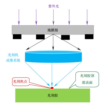
Figure 1.
The diagram of projection lithography
-
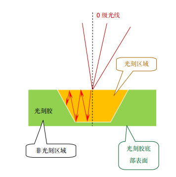
Figure 2.
The reflected light in PR at oblique incidence
-
Figure 3.
The reflected light in the PR when the PR surface is under the lithography focus
-
Figure 4.
The reflected light in the PR when the PR surface is above the lithography focus
-
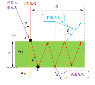
Figure 5.
The reflection light in PR when incident light is vertical incidence
-
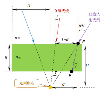
Figure 6.
The reflection light in PR when incident light is oblique incidence
-
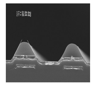
Figure 8.
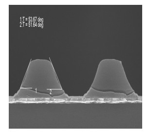
The SEM picture of lithography pattern of normal product after PR surface offset 0 μm
-
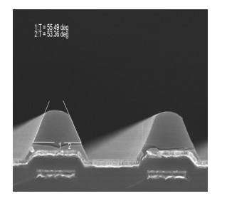
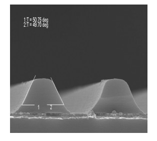
Figure 9.
The SEM picture of lithography pattern of normal product after PR surface offset 8.8 μm
-
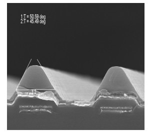
Figure 7.
The SEM picture of lithography pattern of normal product after PR surface offset -8.8 μm
-
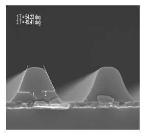
Figure 10.
The SEM picture of lithography pattern of normal product after PR surface offset 18 μm
-
Figure 11.
The SEM picture of lithography pattern of single layer after PR surface offset -6.4 μm
-
Figure 12.
The SEM picture of lithography pattern of single layer after PR surface offset 0 μm
-
Figure 13.
The SEM picture of lithography pattern of single layer after PR surface offset 6.4 μm
-
Figure 14.
The SEM picture of lithography pattern of single layer after PR surface offset 15 μm
-
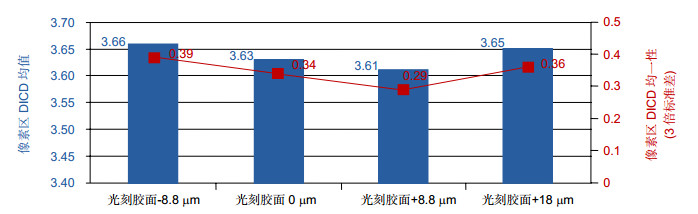
Figure 15.
The DICD of different offset of normal product
-
Figure 16.
The DICD of different offset of single layer


