
 E-mail Alert
 RSS
RSS
| Citation: |
Xin Zhang, Yang Li, Xia Wang, et al. Study on etch process of GaSb-based VCSEL[J]. Opto-Electronic Engineering, 2017, 44(12): 1225-1229. doi: 10.3969/j.issn.1003-501X.2017.12.011

|
Study on etch process of GaSb-based VCSEL
-
Abstract
2 μm~5 μm GaSb-based VCSEL is an ideal light source for atmospheric detection. However, the immaturity of its fabrication technology seriously hinders its development. The undercutting effect is the outstanding etch problem in its fabrication. In this paper, Etching characteristics of GaSb is investigated in detail by use of phosphoric acid plus tartaric acid solution. In order to compare them, we chose concentration ratio of H3PO4:H2O2:C4H6O6:H2O as 1 mL: 1 mL: 0.3 g: 10 mL, 1 mL: 1 mL: 0.6 g: 10 mL, and 1 mL: 1 mL: 1 g: 10 mL, respectively. The testing results from step profiler and scanning electron microscopy (SEM) were compared and analyzed. Etched GaSb in the solution with a concentration ratio of H3PO4:H2O2:C4H6O6:H2O=1:1:0.6:10 shows very good morphology. Undercutting effect was eliminated and a vertical side wall was obtained with no lateral etching. Etching rate is 0.62 μm/min. The perfect etch behavior of GaSb provides a good technical support for laser preparation.-
Keywords:
- Gallium Antimonide /
- VCSEL /
- etching rate /
- surface morphology /
- tartaric acid
-

-
References
[1] Sanchez D, Cerutti L, Tournie E. Mid-IR GaSb-based bipolar cascade VCSELs[J]. IEEE Photonics Technology Letters, 2013, 25(9): 882-884. doi: 10.1109/LPT.2013.2254707 [2] Bachmann A, Kashani-Shirazi K, Arafin S, et al. GaSb-based VCSEL with buried tunnel junction for emission around 2.3μm[J]. IEEE Journal of Selected Topics in Quantum Electronics, 2009, 15(3): 933-940. doi: 10.1109/JSTQE.2009.2013361 [3] Bachmann A, Arafin S, Kashani-Shirazi K, et al. Long wave-length electrically pumped GaSb-based buried tunnel junction VCSELs[J]. Physics Procedia, 2010, 3(2): 1155-1159. doi: 10.1016/j.phpro.2010.01.155 [4] Laaroussi Y, Sanchez D, Cerutti L, et al. Oxide-confined mid-infrared VCSELs[J]. Electronics Letters, 2012, 48(25): 1616-1618. doi: 10.1049/el.2012.3572 [5] Chiu T H, Tsang W T, Ditzenberger J A, et al. Room-temperature operation of InGaAsSb/AlGaSb double heterostructure laser near 2.2 μm prepared by molecular beam epitaxy[J]. Applied Physics Letters, 1986, 49(17): 1051-1052. [6] 田超群. 中红外锑化物激光器工艺中刻蚀研究[D]. 长春: 长春理工大学, 2013. Tian Chaoqun. Etching porcess of mid-infrared antimonide laser[D]. Changchun: Changchun University of Science and Technology, 2013. [7] 张秀, 薄报学, 高欣, 等.脊波导半导体激光器模式特性研究与设计[J].长春理工大学学报(自然科学版), 2011, 34(2): 56-58. Zhang Xiu, Bo Baoxue, Gao Xin, et al. Study and design of the characteristics of ridge waveguide semiconducter lasers[J]. Journal of Changchun University of Science and Technology, 2011, 34(2): 56-58. [8] 董瑞君. GaSb基化合物半导体激光器器件刻蚀工艺研究[D]. 长春: 长春理工大学, 2012. Dong Ruijun. Study of the etching technology for GaSb-based laser[D]. Changchun: Changchun University of Science and Technology, 2012. [9] 陈慧娟, 郭杰, 丁嘉欣, 等. InAs/GaSb超晶格红外探测器台面湿法腐蚀研究[J].微纳电子技术, 2008, 45(5): 298-301. Chen Huijuan, Guo Jie, Ding Jiaxin, et al. Study of mesa etching for a InAs/GaSb superlattice infrared detector[J]. Micronanoelectronic Technology, 2008, 45(5): 298-301. [10] 张雄. 中红外波段锑化物激光器、探测器器件与物理研究[D]. 上海: 上海微系统与信息技术研究所, 2004. Zhang Xiong. Investigation of devices and physics for anti-monide lasers and photodiodes in mid-infrared[D]. Shanghai: Shanghai Institute of Microsystem and Information Technology Research Institute, 2004. [11] 唐田. 锑化物激光器、探测器MBE生长与物理研究[D]. 上海: 上海微系统与信息技术研究所, 2005. Tang Tian. Study on MBE growth and physics of antimonide laser and detector materials[D]. Shanghai: Shanghai Institute of Microsystem and Information Technology Research Institute, 2005. [12] Buglass J G. McLean T D, Parker D G. A controllable etchant for fabrication of gasb devices[J]. Journal of the Electrochemical Society, 1986, 133(12): 2565-2567. doi: 10.1149/1.2108472 [13] Kodarna M, Hasegawa J, Kimata M. Influence of substrate preparation on the morphology of GaSb films grown by molecular beam epitaxy[J]. Journal of the Electrochemical Society, 1985, 132(3): 659-662. doi: 10.1149/1.2113924 [14] 聂晶, 史铁林, 廖广兰, 等. Cr掩模在硅湿法刻蚀中的应用研究[J].半导体技术, 2005, 30(12): 26-28. doi: 10.3969/j.issn.1003-353X.2005.12.009 Nie Jing, Shi Tielin, Liao Guanglian, et al. Application of Cr mask in Si wet etching[J]. Semiconductor Technology, 2005, 30(12): 26-28. doi: 10.3969/j.issn.1003-353X.2005.12.009 [15] 许兆鹏. GaAs、GaP、InP、InGaAsP、AlGaAs、InAlGaAs的化学腐蚀研究[J].固体电子学研究与进展, 1996(1): 56-63. Xu Zhaopeng. Study of wet chemical etching for GaAs, GaP, InP, InGaAsP, AlGaAs and InAlGaAs[J]. Research & Progress of SSE, 1996(1): 56-63. [16] Cao Xin, Thayne I. Novel high uniformity highly reproducible non-selective wet digital gate recess etch process for InP HEMTs[J]. Microelectronic Engineering, 2003, 67-68(1): 333-337. [17] 胡俊达.电子电气设备工艺设计与制造技术[M]. 北京: 机械工业出版社, 2004. [18] Doerschel J, Geissler U. Characterization of extended defects in highly Te-doped〈111〉GaSb single crystals grown by the Czochralski technique[J]. Journal of Crystal Growth, 1992, 121(4): 781-789. doi: 10.1016/0022-0248(92)90586-8 [19] 张雄, 李爱珍, 张永刚, 等.室温工作的AlGaAsSb/InGaAsSb 2μm多量子阱脊波导半导体激光器[J].稀有金属, 2004, 28(3): 574-576. Zhang Xiong, Li Aizhen, Zhang Yonggang, et al. Room temperature AlGaAsSb/InGaAsSb 2 μm ridge-waveguide mul-ti-quantum-well lasers[J]. Chinese Journal of Rare Metals, 2004, 28(3): 574-576. [20] 段成龙, 舒福璋, 宋伟峰, 等.湿法刻蚀及其均匀性技术探讨[J].清洗世界, 2012, 28(11): 33-36. doi: 10.3969/j.issn.1671-8909.2012.11.012 Duan Chenglong, Shu Fuzhang, Song Weifeng, et al. Wet etch and its uniformity technical discuss[J]. Cleaning World, 2012, 28(11): 33-36. doi: 10.3969/j.issn.1671-8909.2012.11.012 -
Overview

2 μm5 μm mid-infrared vertical cavity surface emitting laser (VCSEL), featured with advantages of low power consumption, small divergence angle, no astigmatism circular spot, high modulation bandwidth, wavelength stability,low production cost, and high density ultra-small dimensional packaging, is an ideal light source for the molecular spectrum measurement, biochemical testing, laser radar, thermal imaging and medical diagnosis. For example, in the TDLAS (tunable laser diode absorption spectroscopy test) system for monitoring polluting gases CO, CH4, NH3 and HF, the use of VCSEL as a light source will greatly reduce the complexity and the cost for no beam shaping and easily coupled packaging, and shrink the size of the system. Furthermore, its modulation rate can reach several tens of Gbit/s, so it is considered to be the best alternative device of distributed feedback (DFB) laser in the future. As the GaSb material can cover the entire mid-infrared band, it is the best material system for the development of 2 μm5 μm mid-infrared VCSEL.
GaSb-based VCSEL has become a hot concern over the world because of its promising application. However the immaturity of its fabrication processes seriously hinders its development. E.g., owing to its easily oxidized properties that make etching GaSb not a easy thing, etch process is one of the most key technologies in preparing a GaSb-based VCSEL.
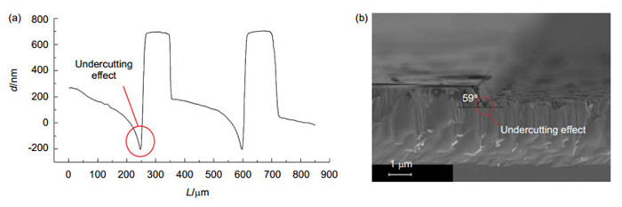
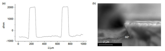
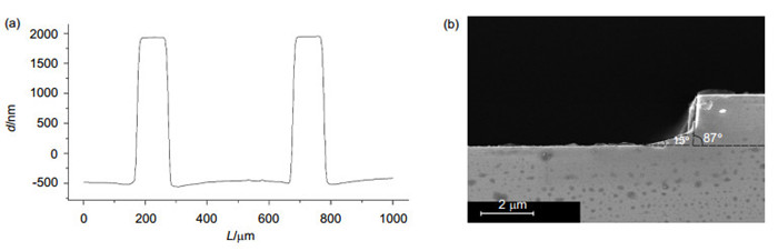
In the previous etching experiments, only the effect of hydrofluoric acid plus tartaric acid etching solution on the corrosion rate was explored, but the surface morphology of the substrate and the undercutting effect was not well analyzed. Etching characteristics of GaSb is investigated in detail by use of phosphoric acid plus tartaric acid solution. In order to compare them, we chose concentration ratio of H3PO4:H2O2:C4H6O6:H2O as 1 mL: 1 mL: 0.3 g: 10 mL, 1 mL: 1 mL: 1 g: 10 mL, and 1 mL: 1 mL: 0.6g: 10 mL, respectively. In order to prevent the corrosion rate of the viscous reaction product formed on the GaSb surface during the etching process, the sample is continuously immersed in the etching solution by a magnetic stirrer to assist in obtaining a constant etching rate.
The experimental results were characterized through scanning electron microscopy (SEM) and so on, and the testing results were compared and analyzed. Etched GaSb in the third group solution (H3PO4:H2O2:C4H6O6:H2O=1:1:0.6:10) shows very good morphology: undercutting effect was eliminated and a vertical side wall was obtained with no lateral etching. Etching rate is 0.62 μm/min. The perfect etch behavior of GaSb provides a good preliminary experimental basis for laser preparation.
-
Access History


Export File
Citation
Xin Zhang, Yang Li, Xia Wang, et al. Study on etch process of GaSb-based VCSEL[J]. Opto-Electronic Engineering, 2017, 44(12): 1225-1229. doi: 10.3969/j.issn.1003-501X.2017.12.011
Format
Content
 DownLoad:
-
Figure 1.
The depth vs. time under different concentration ratio solution.
-
Figure 2.
Cross-sectional view and corrosion surface of sample with P1.
-
Figure 3.
Cross-sectional view and corrosion surface of sample with P2.
-
Figure 4.
Cross-sectional view and corrosion surface of sample with P3.


