
 E-mail Alert
 RSS
RSS
-
摘要:
紫外激光以其波长短、加工精度高、冷加工等特性,在微细制造中具有独特优势,能够有效提高制造品质。近年来,随着现代电子产业的快速发展,其对生产制造的要求不断提高,紫外激光的应用和发展也受到人们的广泛关注。紫外激光在微加工过程中对材料尺寸形状要求小,加工过程灵活可变,产生的热影响区小,能够实现精密复杂结构的加工。本文介绍了紫外激光器的发展过程,并对目前主要用于微加工的两类紫外激光器:准分子激光器和全固态激光器的工作原理和技术特点进行了简要的概述。重点讨论紫外激光在半导体、光学元件和聚合物等领域的技术发展和应用现状,并进一步对未来研究方向进行预测和展望。
Abstract:Ultraviolet (UV) laser has unique advantages in micromachining due to short wavelength, high machining accuracy and cold processing property, leading to improve manufacturing quality effectively. In recent years, electronic industry has been developed rapidly and needs high fabrication requirements. Progress of UV laser has attracted much attention in applications of electronic industry because it can produce complex structures on almost any materials with flexible process and small heat-affected zone. In this review, we summarize the history of UV laser development and fundamental principles as well as characteristics of excimer laser and diode pumped solid state laser, which are two major UV lasers used for micromachining. Moreover, we analyze the development and applications of UV laser in micromachining of semiconductor, optical element and polymer. Finally, we propose some prospects for further research and development in UV laser and its applications.
-
Key words:
- UV laser /
- laser micromachining /
- semiconductor /
- micro-optical element /
- polymer
-

Ultraviolet(UV) laser with its short wavelength, high machining accuracy and cold processing property, has unique advantages in micromachining, and can effectively improve the manufacturing quality. Modern electronic industry has achieved a rapid development in recent years, and sets higher demands in fabricating. UV laser’s progress and applications in electronic industry attracts are attracting broad attention. UV laser can process complex structures on almost any materials with flexible process and small heat-affected zone. It summarizes the development of UV laser. The fundamental principles and characteristics of excimer laser and diode pumped solid state laser are given, which are two major UV lasers used for micromachining. The development and applications of UV laser in the micromachining of semiconductor, optical element and polymer are introduced. It gives some prospects and forecasts about research in the further development.
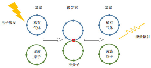
According to different actuating mediums, UV lasers used for micro-machining are majorly classified into two categories, excimer laser and diode pumped solid state laser. The noble gases and halogen elements work as actuating medium in excimer laser. Under the excitation of high-energy electrons, the noble gas atom and halogen element atom combine into excimer. When these excited atoms return to the ground state, it emits energy of a characteristic wavelength. The wavelengths of excimer laser can vary from 126 nm (Ar2) to 650 nm (Xe2F). While in the diode pumped solid state laser, the photons generate from the diode. The origin photons are transmitted into the photonic crystal, where photons excite more photons of fundamental wavelength, which compose fundamental light. Then fundamental light penetrates into the nonlinear frequency doubling crystal, and changes into the second harmonic light with wavelength halved. After several frequency transformations, the origin light finally becomes the expected light of an ultraviolet wavelength.
During the process of laser machining, UV laser carries on processing to materials using the photochemical effects. When UV laser irradiates on the surface of materials, part of photons are absorbed by the electrons of surface. Owing to UV laser’s single photon energy higher than that of chemical bonds between material atoms, the chemical bonds can be directly broken in irradiated area. The materials can be stripped from the surface in the form of gaseous atom or particle, to compete presupposed micro-machining. UV laser has been widely used in the fields of semiconductor, optical element and polymer, for its small heat-affected zone and high machining precision. Application status and developing prospects of UV laser are discussed in this review.
-

-
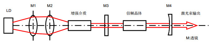
图 2 全固态激光器光路原理图.
Figure 2. Schematic diagram of optical path in diode pumped solid state laser.
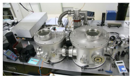
图 3 中国科学院研发的深紫外固态激光源实用化样机.
Figure 3. A prototype of deep UV solid state laser source developed by Chinese academy of sciences.
表 1 Nd:YAG和Nd:YVO4的主要物理性质.
Table 1. The main physical properties of Nd:YAG and Nd:YVO4
晶体 Nd:YAG Nd:YVO4 受激发射截面/(10-20·cm2) 4.3 4.8(∥C), 4.3(⊥C) 荧光寿命/μs 230 97 吸收截面/(10-20·cm2) 7.9 60.1(∥C), 12.0(⊥C) 热导率/(W·m-1·K-1) 11 5.23(∥C), 5.10(⊥C)  下载: 导出CSV
表 2 LBO和KTP的部分物理性质.
Table 2. Partial physical properties of LBO and KTP.
晶体 LBO KTP 光学透过波长范围/nm 160~2600 350~3500 非线性系数/(pm/V) d31=1.05 d33=13.7 激光损伤阈值/(GW/cm2) 18.9 4.6
下载: 导出CSV
-
[1] 楼祺洪.准分子激光器的发展和应用[J].中国激光, 1994, 21(5): 361–364. http://www.opticsjournal.net/abstract.htm?id=OJ100819000037NjPmSp
Lou Qihong. Progress of excimer lasers and its applications[J]. Chinese Journal of Lasers, 1994, 21(5): 361–364. http://www.opticsjournal.net/abstract.htm?id=OJ100819000037NjPmSp
[2] Basov N G, Danilychev V A, Popov Y M, et al. Laser operating in vacuum region of spectrum by excitation of liquid xenon with an electron beam[J]. JETP Letters, 1970, 12(10): 329–331. http://adsabs.harvard.edu/abs/1970ZhPmR..12..473B
[3] Velazco J E, Setser D W. Bound-free emission spectra of diatomic xenon halides[J]. Journal of Chemical Physics, 1975, 62(5): 1990–1991. doi: 10.1063/1.430664
[4] Searles S K, Hart G A. Stimulated emission at 281.8 nm from XeBr[J]. Applied Physics Letters, 1975, 27(4): 243. doi: 10.1063/1.88409
[5] Makarov M K. Once upon a time: a hearty glance over the 30-year history of excimer lasers[J]. Proceedings of SPIE, 2005, 5777: 542–547. doi: 10.1117/12.611113
[6] 尤晨华, 陆祖康, 范琦康, 等.用BBO晶体获得200至218nm的紫外可调谐辐射[J].中国激光, 1989, 16(6): 327–329.
You Chenhua, Lu Zukang, Fan Qikang, et al. Generation of continuosly tunable UV radiation from 200 to 218nm using a BBO crystal[J]. Chinese Journal of Lasers, 1989, 16(6): 327–329.
[7] Kojima T, Konno S, Fujikawa S, et al. 20-W ultraviolet-beam generation by fourth-harmonic generation of an all-solid-state laser[J]. Optics Letters, 2000, 25(1): 58–60. doi: 10.1364/OL.25.000058
[8] Johansson S, Bjurshagen S, Canalias C, et al. An all solid-state UV source based on a frequency quadrupled, passively Q-switched 946 nm laser[J]. Optics Express, 2007, 15(2): 449–458. doi: 10.1364/OE.15.000449
[9] Kimmelma O P, Tittonen I, Buchter S C. Short pulse, diode pumped, passively Q-switched Nd: YAG laser at 946 nm quadrupled for UV production[J]. Journal of the European Optical Society-Rapid Publications, 2008, 3: 08008. doi: 10.2971/jeos.2008.08008
[10] Deyra L, Martial I, Didierjean J, et al. Deep-UV 236.5 nm laser by fourth-harmonic generation of a single-crystal fiber Nd: YAG oscillator[J]. Optics Letters, 2014, 39(8): 2236–2239. doi: 10.1364/OL.39.002236
[11] 许祖彦.深紫外全固态激光源[J].中国激光, 2009, 36(7): 1619–1624. http://www.opticsjournal.net/abstract.htm?aid=OJ090716000003B8EaGd
Xu Zuyan. Deep-ultraviolet diode-pumped solid-state laser[J]. Chinese Journal of Lasers, 2009, 36(7): 1619–1624. http://www.opticsjournal.net/abstract.htm?aid=OJ090716000003B8EaGd
[12] 陈创天, 许祖彦, 吕军华, 等. 一种非线性光学晶体激光变频耦合器: CN1172411C[P]. 2004-10-20.
Chen Chuangtian, Xu Zuyan, Lü Junhua, et al. Variable-frequency laser coupler with non-linear optical crystal: CN1172411C[P]. 2004-10-20.
[13] 许祖彦, 王保山, 宗楠, 等. 直接倍频实现波长160~170nm全固态深紫外激光的装置: CN102957083B[P]. 2014-09-03.
Xu Zuyan, Wang Baoshan, Zong Nan, et al. Device for implementing all-solid-state deep ultraviolet laser with wavelength of 160-170 nm through direct frequency doubling: CN102957083B [P]. 2014-09-03.
[14] Simon P, Ihlemann J. Ablation of submicron structures on metals and semiconductors by femtosecond UV-laser pulses[J].Applied Surface Science, 1997, 109–110: 25–29. doi: 10.1016/S0169-4332(96)00615-0
[15] Chen Chengyan, Chao C Y, Wu Z K, et al. Semiconductor material process with UV laser irradiation[C]//Proceedings of Summaries of Papers Presented at the Lasers and Electro-Optics, San Francisco, CA, USA, 1998: 153–154.
[16] He Liming. An investigation of three-dimensional construction methods in the micromachining of silicon surfaces with an ultraviolet laser[J]. Chinese Journal of Lasers, 1998, 7(5): 339–444. http://www.cnki.com.cn/Article/CJFDTotal-ZGJY805.009.htm
[17] 马炳和, 苑伟政, 李铁军, 等.准分子激光直接刻蚀单晶硅研究[J].西北工业大学学报, 2000, 18(3): 491–495. http://www.wanfangdata.com.cn/details/detail.do?_type=perio&id=xbgydxxb200003037
Ma Binghe, Yuan Weizheng, Li Tiejun, et al. Micromachining of monocrystal silicon by excimer laser direct etching[J]. Journal of Northwestern Polytechnical University, 2000, 18(3): 491–495. http://www.wanfangdata.com.cn/details/detail.do?_type=perio&id=xbgydxxb200003037
[18] Furukawa Y, Sasahara H, Kakuta A, et al. Principal factors affecting the sub-micrometer grooving mechanism of SiC thin layers by a 355 nm UV laser[J]. CIRP Annals, 2006, 55(1): 573–576. doi: 10.1016/S0007-8506(07)60485-5
[19] Gu E, Howard H, Conneely A, et al. Microfabrication in free-standing gallium nitride using UV laser micromachining[J]. Applied Surface Science, 2006, 252(13): 4897–4901. doi: 10.1016/j.apsusc.2005.07.117
[20] 朱冀梁, 张恒, 陈林森, 等.多光束纳秒紫外激光制作硅表面微结构[J].光子学报, 2009, 38(10): 2463–2467. https://www.wenkuxiazai.com/doc/0cc91ed433d4b14e8524684d.html
Zhu Jiliang, Zhang Heng, Chen Linsen, et al. Fabricating microstructure on the surface of silicon using multiple beam of nanosecond UV laser[J]. Acta Photonica Sinica, 2009, 38(10): 2463–2467. https://www.wenkuxiazai.com/doc/0cc91ed433d4b14e8524684d.html
[21] 杨雄. 单晶硅紫外激光微加工工艺研究[D]. 武汉: 华中科技大学, 2011.
Yang Xiong. A study on UV laser micro-machining single-crystal silicon[D]. Wuhan: Huazhong University of Science and Technology, 2011.
[22] 齐立涛, 刘文海. 266 nm紫外固体激光在碳化硅晶片上的微结构加工[J].黑龙江科技大学学报, 2017, 27(2): 176–180. http://www.opticsjournal.net/Journals/zgjg.htm?action=down
Qi Litao, Liu Wenhai. Experimental investigation on 266 nm UV solid-state laser micromachining of microstructures on SiC wafer[J].Journal of Heilongjiang University of Science and Technology, 2017, 27(2): 176–180. http://www.opticsjournal.net/Journals/zgjg.htm?action=down
[23] 楼祺洪, 章琳, 叶震寰, 等.紫外激光切割Si片的实验研究[J].激光技术, 2002, 26(4): 250–251, 254. http://www.cqvip.com/QK/92283X/200204/6674260.html
Lou Qihong, Zhang Lin, Ye Zhenhuan, et al. Experimental research on Si cutting by using UV excimer laser[J]. Laser Technology, 2002, 26(4): 250–251, 254. http://www.cqvip.com/QK/92283X/200204/6674260.html
[24] Chen Taichen, Robert B D. Parametric studies on pulsed near ultraviolet frequency tripled Nd: YAG laser micromachining of sapphire and silicon[J]. Journal of Materials Processing Technology, 2005, 169(2): 214–218. doi: 10.1016/j.jmatprotec.2005.03.023
[25] Tom C, Edward C R, Corey D. High-power UV laser machining of silicon wafers[J]. Proceedings of SPIE, 2003, 5063: 495–500. doi: 10.1117/12.540931
[26] Gu E, Jeon C W, Choi H W, et al. Micromachining and dicing of sapphire, gallium nitride and micro LED devices with UV copper vapour laser[J]. Thin Solid Films, 2004, 453–454: 462–466. https://www.sciencedirect.com/science/article/pii/S0040609003017383
[27] Baird B W, Hainsey R F, Peng X, et al. Advances in laser processing of microelectronics[J]. Proceedings of SPIE, 2007, 6451: 64511K. doi: 10.1117/12.713213
[28] Ihlemann J, Wolff B, Simon P. Nanosecond and femtosecond excimer laser ablation of fused silica[J]. Applied Physics A, 1992, 54(4): 363–368. doi: 10.1007/BF00324203
[29] Zhang J, Sugioka K, Takahashi T, et al. Dual-beam ablation of fused silica by multiwavelength excitation process using KrF excimer and F2 lasers[J]. Applied Physics A, 2000, 71(1): 23–26. https://link.springer.com/content/pdf/10.1007/PL00021086.pdf
[30] Herman P R, Marjoribanks R S, Oettl A, et al. Laser shaping of photonic materials: deep-ultraviolet and ultrafast lasers[J]. Applied Surface Science, 2000, 154–155: 577–586. doi: 10.1016/S0169-4332(99)00463-8
[31] Sugioka K, Akane T, Obata K, et al. Multiwavelength excitation processing using F2 and KrF excimer lasers for precision microfabrication of hard materials[J]. Applied Surface Science, 2002, 197–198: 814–821. doi: 10.1016/S0169-4332(02)00465-8
[32] 王汕. 激光刻蚀抛光石英玻璃工艺研究[D]. 武汉: 华中科技大学, 2012.
Wang Shan. A study on laser etching and polishing quartz glasses technology[D]. Wuhan: Huazhong University of Science and Technology, 2012.
[33] 杨桂栓, 陈涛, 陈虹. 248 nm准分子激光刻蚀的无裂损石英玻璃表面微通道[J].中国激光, 2017, 44(9): 0902004. http://www.opticsjournal.net/Articles/abstract?aid=OJ171012000156JfMiOl
Yang Guishuan, Chen Tao, Chen Hong. Crack-free silica glass surface micro-grooves etched by 248 nm excimer lasers[J]. Chinese Journal of Lasers, 2017, 44(9): 0902004. http://www.opticsjournal.net/Articles/abstract?aid=OJ171012000156JfMiOl
[34] 邵勇, 孙树峰, 廖慧鹏, 等.激光诱导等离子体刻蚀Pyrex7740玻璃工艺研究[J].应用激光, 2017, 37(5): 704–708.
Shao Yong, Sun Shufeng, Liao Huipeng, et al. Process study on laser induced plasma etching of pyrex7740 glass[J]. Applied Laser, 2017, 37(5): 704–708.
[35] Delmdahl R, Pätzel R. Pulsed laser deposition—UV laser sources and applications[J]. Applied Physics A, 2008, 93(3): 611–615. doi: 10.1007/s00339-008-4716-7
[36] 赵泽宇, 侯德胜, 董小春, 等.准分子激光刻蚀聚碳酸酯材料研究[J].光电工程, 2004, 31(2): 4–7. https://www.wenkuxiazai.com/doc/5a7353868762caaedd33d4f9.html
Zhao Zeyu, Hou Desheng, Dong Xiaochun, et al. Research on etching properties of polycarbonate by KrF excimer laser[J]. Opto-Electronic Engineering, 2004, 31(2): 4–7. https://www.wenkuxiazai.com/doc/5a7353868762caaedd33d4f9.html
[37] Aguilar C A, Lu Yi, Mao S, et al. Direct micro-patterning of biodegradable polymers using ultraviolet and femtosecond lasers[J]. Biomaterials, 2005, 26(36): 7642–7649. doi: 10.1016/j.biomaterials.2005.04.053
[38] Menoni C S, Brizuela F, Brewer C, et al. Nanoscale resolution microscopy and ablation with extreme ultraviolet lasers[C]//Proceedings of the 20th Annual Meeting of the IEEE Lasers and Electro-Optics Society, Lake Buena Vista, FL, UAS, 2007: 488–489.
[39] Tiaw K S, Hong M H, Teoh S H. Precision laser micro-processing of polymers[J]. Journal of Alloys and Compounds, 2008, 449(1–2): 228–231. doi: 10.1016/j.jallcom.2006.01.145
[40] 王素焕, 刘建国, 吕铭, 等.脉冲紫外激光改性对聚碳酸酯表面润湿性能的影响[J].光电工程, 2013, 40(7): 77–82. http://doi.wanfangdata.com.cn/10.3969/j.issn.1003-501X.2013.07.013
Wang Suhuan, Liu Jianguo, Lü Ming, et al. The effect of pulse ultraviolet laser modification on the surface wetting property of polycarbonate[J]. Opto-Electronic Engineering, 2013, 40(7): 77–82. http://doi.wanfangdata.com.cn/10.3969/j.issn.1003-501X.2013.07.013
[41] Park C, Shin B S, Kang M S, et al. Experimental study on micro-porous patterning using UV pulse laser hybrid process with chemical foaming agent[J]. International Journal of Precision Engineering and Manufacturing, 2015, 16(7): 1385–1390. doi: 10.1007/s12541-015-0182-2
[42] Lei Weisheng, Davignon J. Solid state UV laser technology for electronic packaging applications[J].Proceedings of SPIE, 2005, 5629: 314–326. doi: 10.1117/12.571520
[43] 张菲, 段军, 曾晓雁, 等. 355 nm紫外激光加工柔性线路板盲孔的研究[J].中国激光, 2009, 36(12): 3143–3148. http://www.cqvip.com/QK/95389X/200912/32405575.html
Zhang Fei, Duan Jun, Zeng Xiaoyan, et al. Study of blind holes drilling on flexible circuit board using 355nm UV laser[J].Chinese Journal of Lasers, 2009, 36(12): 3143–3148. http://www.cqvip.com/QK/95389X/200912/32405575.html
[44] 张林华, 杨永强, 来克娴.激光技术在大规模集成电路中的应用及展望[J].激光与光电子学进展, 2005, 42(6): 48–55. http://www.cqvip.com/QK/92536A/200506/15785885.html
Zhang Linhua, Yang Yongqiang, Lai Kexian. Laser in large-scale integrated circuit: application and prospects[J]. Laser & Optoelectronics Progress, 2005, 42(6): 48–55. http://www.cqvip.com/QK/92536A/200506/15785885.html
[45] 凌磊, 楼祺洪, 叶震寰, 等.紫外激光刻蚀多层线路板初步研究[J].中国激光, 2003, 30(10): 953–955. doi: 10.3321/j.issn:0258-7025.2003.10.021
Ling Lei, Lou Qihong, Ye Zhenhuan, et al. Ablation of circuit board by pulsed UV laser[J]. Chinese Journal of Lasers, 2003, 30(10): 953–955. doi: 10.3321/j.issn:0258-7025.2003.10.021
-
 点击扫一扫
点击扫一扫
图(10)
表(2)
计量
- 文章访问数: 9980
- PDF下载数: 4702
- 施引文献: 0


