
 E-mail Alert
 RSS
RSS
| Citation: |
Cao Yaoyu, Xie Fei, Zhang Pengda, et al. Dual‐beam super‐resolution direct laser writing nanofabrication technology[J]. Opto-Electronic Engineering, 2017, 44(12): 1133-1145. doi: 10.3969/j.issn.1003-501X.2017.12.001

|
Dual‐beam super‐resolution direct laser writing nanofabrication technology
-
Abstract
With the development of nanotechnology, emerging nanotechniques compel dramatically increasing demands on nanostructures' fabrication. As an important three-dimensional micro/nanostructures' fabrication method, direct laser writing has been widely applied in various modern scientific technological fields. To realize three dimensional micro/nanostructures, dual-beam super-resolution direct laser writing technique, combined with two-photon polymerization (TPP) method and stimulated emission depletion (STED) principle, has successfully realized resolution beyond optical diffraction limit, and uphold exceptional 3D nanofabrication scheme. The principle of dual-beam super-resolution laser direct writing and recent progress in improving line width and resolution have been demonstrated in the review. We have also summarized emerging applications of dual-beam super-resolution laser direct writing in relevant fields. Eventually, challenges in how to fulfill low-cost, high efficiency, large area and multi-functional materials' fabrication and its future development are discussed. -

-
References
[1] Fischer J, Wegener M. Three-dimensional optical laser lithog-raphy beyond the diffraction limit[J]. Laser & Photonics Re-views, 2013, 7(1): 22–44. [2] Liu Liqin, Zhang Xiaohu, Zhao Zeyu, et al. Batch fabrication of metasurface holograms enabled by plasmonic cavity lithogra-phy[J]. Advanced Optical Materials, 2017, 5(21): 1700429. doi: 10.1002/adom.v5.21 [3] Luo Xiangang. Principles of electromagnetic waves in metasurfaces[J]. Science China Physics, Mechanics & Astronomy, 2015, 58(9): 594201. [4] Gao Ping, Yao Na, Wang Changtao, et al. Enhancing aspect profile of half-pitch 32 nm and 22 nm lithography with plasmonic cavity lens[J]. Applied Physics Letters, 2015, 106(9): 093110. doi: 10.1063/1.4914000 [5] Andrew T L, Tsai H Y, Menon R. Confining light to deep sub-wavelength dimensions to enable optical nanopatterning[J]. Science, 2009, 324(5929): 917–921. doi: 10.1126/science.1167704 [6] 刘立鹏, 周明, 戴起勋, 等.飞秒激光三维微细加工技术[J].光电工程, 2005, 32(4): 93–96. Liu Lipeng, Zhou Ming, Dai Qixun, et al. Three-dimensional micro-fabrication by femtosecond laser[J]. Opto-Electronic En-gineering, 2005, 32(4): 93–96. [7] 田小永, 尹丽仙, 李涤尘.三维超材料制造技术现状与趋势[J].光电工程, 2017, 44(1): 69–76. Tian Xiaoyong, Yin Lixian, Li Dichen. Current situation and trend of fabrication technologies for three-dimensional metamaterials[J]. Opto-Electronic Engineering, 2017, 44(1): 69–76. [8] de Miguel G, Duocastella M, Vicidomini G, et al. λ/20 axial control in 2.5D polymerized structures fabricated with DLW lithography[J]. Optics Express, 2015, 23(19): 24850–24858. doi: 10.1364/OE.23.024850 [9] Kawata S, Sun Hongbo, Tanaka T, et al. Finer features for functional microdevices[J]. Nature, 2001, 412(6848): 697–698. doi: 10.1038/35089130 [10] Hell S W, Wichmann J. Breaking the diffraction resolution limit by stimulated emission: stimulated-emission-depletion fluores-cence microscopy[J]. Optics Letters, 1994, 19:780–782. [11] Elmeranta M, Vicidomini G, Duocastella M, et al. Characteriza-tion of nanostructures fabricated with two-beam DLW lithography using STED microscopy[J]. Optical Materials Express, 2016, 6(10): 3169–3179. doi: 10.1364/OME.6.003169 [12] Harke B, Keller J, Ullal C K, et al. Resolution scaling in STED microscopy[J]. Optics Express, 2008, 16(6): 4154–4162. doi: 10.1364/OE.16.004154 [13] Klar T A, Wollhofen R, Jacak J. Sub-Abbe resolution: from STED microscopy to STED lithography[J]. Physica Scripta, 2014, 162: 014049. [14] Barner-Kowollik C, Bastmeyer M, Blasco E, et al. 3D laser micro-and nanoprinting: challenges for chemistry[J]. Angewandte Chemie International Edition, 2017, 56(50): 15828–15845. doi: 10.1002/anie.201704695 [15] Malinauskas M, Žukauskas A, Hasegawa S, et al. Ultrafast laser processing of materials: from science to industry[J]. Light: Science & Applications, 2016, 5(8): e16133. [16] Glubokov D A, Sychev V V, Vitukhnovsky A G, et al. Photonic crystal fibre-based light source for STED lithography[J]. Quantum Electronics, 2013, 43(6): 588–590. doi: 10.1070/QE2013v043n06ABEH015059 [17] Mueller J B, Fischer J, Mayer F, et al. Polymerization kinetics in three-dimensional direct laser writing[J]. Advanced Materials, 2014, 26(38): 6566–6571. doi: 10.1002/adma.v26.38 [18] Harke B, Bianchini P, Brandi F, et al. Photopolymerization inhibition dynamics for sub-diffraction direct laser writing lithography[J]. ChemPhysChem, 2012, 13(6): 1429–1434. doi: 10.1002/cphc.v13.6 [19] Gan Zongsong, Cao Yaoyu, Jia Baohua, et al. Dynamic modeling of superresolution photoinduced-inhibition nanolithography[J]. Optics Express, 2012, 20(15): 16871–16879. doi: 10.1364/OE.20.016871 [20] Cao Yaoyu, Gan Zongsong, Jia Baohua, et al. High-photosensitive resin for super-resolution direct-laser-writing based on photoinhibited polymerization[J]. Optics Express, 2011, 19(20): 19486–19494. doi: 10.1364/OE.19.019486 [21] Gan Zongsong, Cao Yaoyu, Evans R A, et al. Three-dimensional deep sub-diffraction optical beam lithography with 9 nm feature size[J]. Nature Communication, 2013, 4: 2061. [22] Scott T F, Kowalski B A, Sullivan A C, et al. Two-color sin-gle-photon photoinitiation and photoinhibition for subdiffraction photolithography[J]. Science, 2009, 324(5929): 913–917. doi: 10.1126/science.1167610 [23] Li Linjie, Gattass R R, Gershgoren E, et al. Achieving λ/20 Resolution by one-color initiation and deactivation of polymerization[J]. Science, 2009, 324(5929): 910–913. doi: 10.1126/science.1168996 [24] Fischer J, von Freymann G, Wegener M. The materials chal-lenge in diffraction-unlimited direct-laser-writing optical lithog-raphy[J]. Advanced Materials, 2010, 22(32): 3578–3582. doi: 10.1002/adma.201000892 [25] Fischer J, Wegener M. Ultrafast polymerization inhibition by stimulated emission depletion for three-dimensional nanolithography[J]. Advanced Materials, 2012, 24(10): OP65–OP69. [26] Mueller P, Zieger M M, Richter B, et al. Molecular switch for sub-diffraction laser lithography by photoenol intermediate-state cis-trans isomerization[J]. ACS Nano, 2017, 11(6): 6396–6403. doi: 10.1021/acsnano.7b02820 [27] Wollhofen R, Katzmann J, Hrelescu C, et al. 120 nm resolution and 55 nm structure size in STED-lithography[J]. Optics Express, 2013, 21(9): 10831–10840. doi: 10.1364/OE.21.010831 [28] Wollhofen R, Buchegger B, Eder C, et al. Functional photore-sists for sub-diffraction stimulated emission depletion lithogra-phy[J]. Optical Materials Express, 2017, 7(7): 2538–2559. doi: 10.1364/OME.7.002538 [29] He Xiaolong, Datta A, Nam W, et al. Sub-diffraction limited writing based on laser induced periodic surface structures (LIPSS)[J]. Science Report, 2016, 6: 35035. doi: 10.1038/srep35035 [30] Yang Liang, Qian Dongdong, Xin Chen, et al. Direct laser writing of complex microtubes using femtosecond vortex beams[J]. Applied Physics Letters, 2017, 110(22): 221103. doi: 10.1063/1.4984744 [31] Frölich A, Fischer J, Zebrowski T, et al. Titania woodpiles with complete three-dimensional photonic bandgaps in the visible[J]. Advanced Materials, 2013, 25(26): 3588–3592. doi: 10.1002/adma.201300896 [32] Kaschke J, Wegener M. Gold triple-helix mid-infrared met-amaterial by STED-inspired laser lithography[J]. Optics Letters, 2015, 40(17): 3986–3989. doi: 10.1364/OL.40.003986 [33] Gan Zongsong, Turner M D, Gu Min. Biomimetic gyroid nanostructures exceeding their natural origins[J]. Science Ad-vances, 2016, 2(5): e1600084. doi: 10.1126/sciadv.1600084 [34] Gu Min, Li Xiangping, Cao Yaoyu. Optical storage arrays: a perspective for future big data storage[J]. Light: Science & Applications, 2014, 3(5): e177. [35] Li Xiangping, Cao Yaoyu, Tian Nian, et al. Multifocal optical nanoscopy for big data recording at 30 TB capacity and giga-bits/second data rate[J]. Optica, 2015, 2(6): 567–570. doi: 10.1364/OPTICA.2.000567 [36] Wiesbauer M, Wollhofen R, Vasic B, et al. Nano-anchors with single protein capacity produced with STED lithography[J]. Nano Letters, 2013, 13(11): 5672−5678. doi: 10.1021/nl4033523 [37] Wolfesberger C, Wollhofen R, Buchegger B, et al. Streptavidin functionalized polymer nanodots fabricated by visible light li-thography[J]. Journal of Nanobiotechnology, 2015, 13: 27. doi: 10.1186/s12951-015-0084-6 [38] Buchegger B, Kreutzer J, Plochberger B, et al. Stimulated emission depletion lithography with mercapto-functional polymers[J]. ACS Nano, 2016, 10(2): 1954–1959. doi: 10.1021/acsnano.5b05863 [39] Vasilantonakis N, Terzaki K, Sakellari I, et al. Three-dimensional metallic photonic crystals with optical bandgaps[J]. Advanced Materials, 2012, 24(8): 1101−1105. doi: 10.1002/adma.201104778 [40] Ovsianikov A, Mironov V, Stampfl J, et al. Engineering 3D cell-culture matrices: multiphoton processing technologies for biological and tissue engineering applications[J]. Expert Review of Medical Devices, 2012, 9(6): 613−633. doi: 10.1586/erd.12.48 [41] Selimović S, Oh J, Bae H, et al. Microscale strategies for generating cell-encapsulating hydrogels[J]. Polymers, 2012, 4(3): 1554−1579. doi: 10.3390/polym4031554 [42] Klein F, Richter B, Striebel T, et al. Two-component polymer scaffolds for controlled three-dimensional cell culture[J]. Ad-vanced Materials, 2011, 23(11): 1341−1345. doi: 10.1002/adma.v23.11 [43] Scheiwe A C, Frank S C, Autenrieth T J, et al. Subcellular stretch-induced cytoskeletal response of single fibroblasts within 3D designer scaffolds[J]. Biomaterials, 2015, 44: 186−194. doi: 10.1016/j.biomaterials.2014.12.018 [44] Wickberg A, Mueller J B, Mange Y J, et al. Three-dimensional micro-printing of temperature sensors based on up-conversion luminescence[J]. Applied Physics Letters, 2015, 106(13): 133103. doi: 10.1063/1.4916222 [45] Farahani R D, Dubé M, Therriault D. Three-dimensional printing of multifunctional nanocomposites: manufacturing techniques and applications[J]. Advanced Materials, 2016, 28(28): 5794–5821. doi: 10.1002/adma.201506215 [46] Malinauskas M, Baltriukiene D, Kraniauskas A, et al. In vitro and in vivo biocompatibility study on laser 3D microstructurable polymers[J]. Applied Physics A: Materials Science & Processing, 2012, 108(3): 751−759. [47] Kumpfmueller J, Stadlmann K, Li Zhiquan, et al. Two-photon-induced thiol-ene polymerization as a fabrication tool for flexible optical waveguides[J]. Designed Monomers and Polymers, 2014, 17(4): 390−400. doi: 10.1080/15685551.2013.840515 [48] Quick A S, Fischer J, Richter B, et al. Preparation of reactive three-dimensional microstructures via direct laser writing and thiol-ene chemistry[J]. Macromolecular Rapid Communications, 2013, 34(4): 335−340. doi: 10.1002/marc.v34.4 [49] Terzaki K, Vasilantonakis N, Gaidukeviciute A, et al. 3D con-ducting nanostructures fabricated using direct laser writing[J]. Optics Materials Express, 2011, 1(4): 586−597. doi: 10.1364/OME.1.000586 [50] Jin Jinjin, Pu Mingbo, Wang Yanqin, et al. Multi-channel vortex beam generation by simultaneous amplitude and phase modulation with two-dimensional metamaterial[J]. Advanced Materials Technologies, 2017, 2(2): 1600201. doi: 10.1002/admt.201600201 [51] Formanek F, Takeyasu N, Tanaka T. Three-dimensional fabrication of metallic nanostructures over large areas by two-photon polymerization[J]. Optics Express, 2006, 14(2): 800–809. doi: 10.1364/OPEX.14.000800 -
Overview

Abstract: With the development of nanotechnology, emerging nanotechniques compel dramatically increasing demands on fabrication technique for realizing nanostructures. As an important approach, direct laser writing has demonstrated extraordinary capabilities in fabricating three-dimensional (3D) micro/nanostructure, which stems from spatially resolved focal spot by tightly focusing laser beams. The unique 3D feature fabrication allows volumetrically integrating multiple electro- or opto-functionalities in micro/nanodevices, and thus, is promising for advancing various modern scientific technological fields such as next generation of micromechanics and opto-nanodevices. However, the feature size of structures as fabricated as well as resolution in fabrication is subject to a fundamental limit set by the diffraction nature of light. In this regard, the minimum feature size of structures as fabricated is commonly constrained from half the wavelength of the light output by the laser source. To improve resolution beyond the optical diffraction limit, in this review, we introduce a dual-beam super-resolution direct laser writing technique. Combined with two-photon polymerization (TPP) method and stimulated emission depletion (STED) principle, the technique has successfully realized resolution much finer than its counterpart being obtained based on Abbe’s law, and uphold exceptional 3D nanofabrication scheme. The principle of dual-beam super-resolution laser direct writing and recent progress in improving line width and resolution have been demonstrated in the review. In general, two beams are employed in the fabrication. One beam, so called initiating beam, is used to initiate optical reactions such as photo-polymerization, and the other, namely the inhibiting beam, is used to inhibit the optical reaction. While the initiating beam is modulated to Gaussian shape, the inhibiting beam can be shaped into Laguerre-Gaussian mode with zero light intensity in the center. By overlapping these two beams in the focal region, the inhibiting can inhibit the fabrication in its out ring, leaving the center of the initiating beam in function. As a result, a super-resolved focal spot can be obtained with tuning the intensity ratio of the two beams. To further improve resolution to nanoscale, delicate design to the photoresin material and the focal field is required. For instance, optimizing the inhibition efficiency upon the exposure to the inhibiting beam enables 9 nm free-standing line equivalent to one eighty-ninth of the wavelength of the initiating beam. Moreover, we have also summarized emerging applications of dual-beam super-resolution laser direct writing in relevant fields, such as opto-devices with photonic band gap in visible region and biology. Eventually, challenges in how to fulfill low-cost, high efficiency, large area and multi-functional materials’ fabrication and its future development are discussed.
-
Access History

Figures(13)
Tables(1)
Article Metrics


Export File
Citation
Cao Yaoyu, Xie Fei, Zhang Pengda, et al. Dual‐beam super‐resolution direct laser writing nanofabrication technology[J]. Opto-Electronic Engineering, 2017, 44(12): 1133-1145. doi: 10.3969/j.issn.1003-501X.2017.12.001
Format
Content
 DownLoad:


-
Figure 1.
Schematic diagram of dual-beam super-resolution fabrication.
-
Figure 2.
Simulations of phase modulation point spread functions of laser focus. (a) Without phase-plate. (b) With 2π spiral phase-plate. (c) With annular phase-plate.
-
Figure 3.
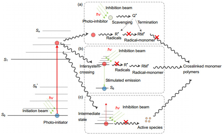
Schematic diagram of the molecular states and transitions for different depletion mechanisms based on photo-initiating and photo-inhibiting principle. (a) Photo-induced chain radical inhibition (PCI). Photoinitiator molecules are excited and generate radicals(R•) which lead to monomer photopolymerization, photoinhibitor molecules are excited and generate radicals(Q•) to clear radicals(R•), thus to terminate propagating polymer chains(RM•). (b) Photo-induced stimulated emission inhibition(PSI). Photoinitiator molecules are excited to active excitation station by two-photon absorption, via intersystem crossing reaching to triplet state, and generate radicals(R•) leading to photopolymerization, the inhibition beam deactivates photointiator molecules by stimulated emission, thus to inhibit radicals' generation and propagating polymer chains(RM•). (c) Photo-induced intermediate state inhibition(PMI). Photoinitiator molecules are excited by two-photon absorption to a long-lived intermediate state, with some active species generation, leading to photopolymerization. Under inhibition laser irrigation, the intermediate state is deactivated and inhibit the cross-linking polymerization[1, 13].
-
Figure 4.
(a) SEM images of voxels created with inhibition beam powers of 0 mW, 17 mW, 34 mW, 50 mW, 84 mW and 100 mW (left to right, top to bottom). (b) Dependence of the height and aspect ratio of voxels on the power of the deactivation beam. (c) Three-dimensional tower with rings structure [22].
-
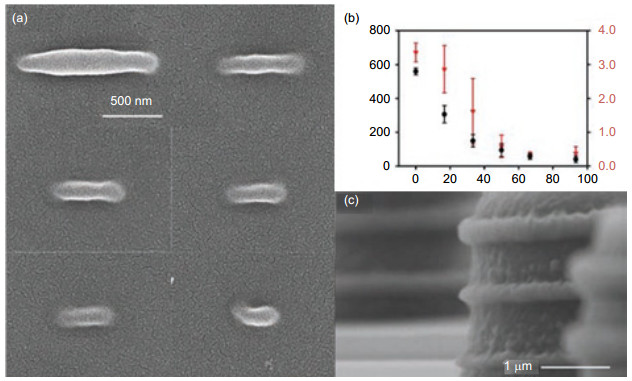
Figure 5.
SEM of polymer voxels features with donut-shaped inhibition laser irradiation. The excitation power was held at 10 μW while the depletion power was progressively increased, from left to right, 0 μW, 1 μW, 2.5 μW, 10 μW and 100 μW. (b) Fitting curve of voxels fabricated with 10 μW of excitation power and 110 μW of depletion power. (c) Polymer column fabricated by using the same conditions as Fig. 5(b), at a velocity of 0.125 μm/s for 3 μm[21].
-
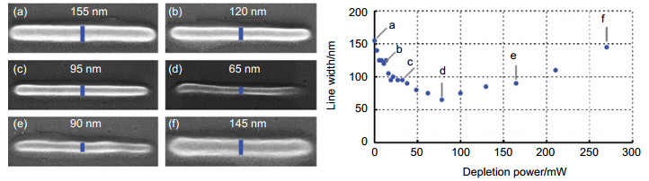
Figure 6.
Polymer linewidth versus power of the continuous-wave 532 nm wavelength depletion beam. The power of the two-photon excitation beam centered around 810 nm wavelength is fixed to 13.5 mW. (a)~(f) Exhibit electron micrographs illustrating the raw data underlying the data points[23].
-
Figure 7.
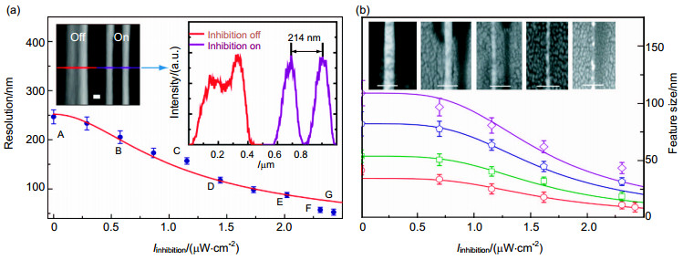
(a) Two-line resolution versus the intensity of the inhibition laser beam, line resolution gradually improved with depletion power increasing, reaching 52 nm in G dot. (b) Feature size of free-standing lines versus the intensity of the inhibition beam, feature size gradually decreased with depletion power increasing, reaching 9 nm in E dot[20].
-
Figure 8.
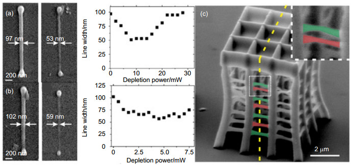
(a) SEM images of MPOEA/PETA photoresist linewidth without depletion power and minimum linewidth with depletion power increasing, relationship between linewidth and depletion power increasing (right). (b) SEM images of CEA/PETA photoresist linewidth without depletion power and minimum linewidth with depletion power increasing, relationship between linewidth and depletion power increasing (right). (c) Confocal fluorescence images of the 3D composite multi-layer structure by dual-beam fabricating two different photoresists[28].
-
Figure 9.
Schematic diagram of fabrication and processing of three-dimensional photonic bandgap crystals[31].
-
Figure 10.
(a) Scanning electron micrographs of the polymer helices structures. (b) Scanning electron micrographs of the final gold helices structures. (c) Arrays of single helices fabricated on the same substrate and employing the same fabrication process. (d) Scanning electron micrograph of single helices as previously fabricated by conventional direct laser writing[32].
-
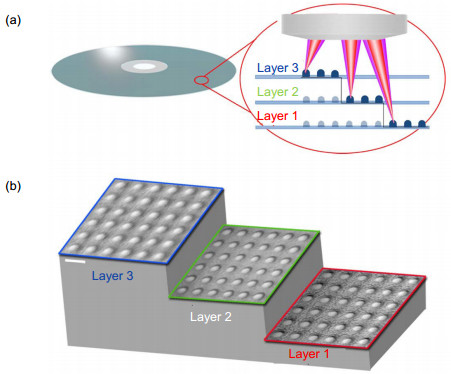
Figure 11.
Demonstration of 3D parallelized recording through a volumetric superresolved multifocal array. (a) Scheme of 3D parallelized recording on the prefabricated multilayered structure with a layer separation of 1.5 μm. (b) SEM images of three layers of bit arrays recorded by superresolved multifocal array with a bit separation of 200 nm and uniform bit size of 80 nm[35].
-
Figure 12.
(a) Nanoanchors fabricated by dual-beam super-resolution fabrication. Top: SEM image. Middle: auto fluorescence of the nanoanchors. Bottom: no auto fluorescence is detectable using 647 nm excitation. (b), (c) Under 647 nm excitation, fluorescence distribution of Atto655-labeled antibodies in nanoanchors array before washing and after washing. (d) Statistical distribution of fluorescence intensity counts per fluorescent spot during 5 ms collection time, obtained from: red sparsely and randomly distributed antibodies and blue from nanoanchors loaded with antibodies[36].
-
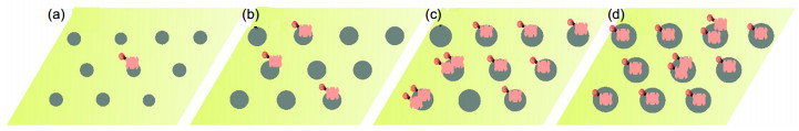
Figure 13.
(a) Sketch of nanostructured dots (nanoanchors) incubated with fluorescent streptavidin. Only 10% of all dots were covered with proteins. (b) Sketch of fabricated dots having ~30% average streptavidin loading per dot. (c), (d) are sketches of the largest fabricated dots with over 80% and 100% streptavidin coverage[37].


