
 E-mail Alert
 RSS
RSS
-
Abstract:
A tunable plasmofluidic lens consisting of nanoslit arrays on a metal film is proposed for subwavelength imaging in far field at different wavelengths. The nanoslit arrays with constant depths but varying widths could generate desired optical phase retardations based on the propagation property of the surface plasmon polaritons (SPPs) through the metal-dielectric-metal (MDM) nanoslit waveguide. We demonstrate the tunability of the plasmofluidic lens for subwavelength imaging by changing the surrounding dielectric fluid. This work provides a novel approach for developing integrative tunable plasmofluidic lens for a variety of lab-on-chip applications.

-
Key words:
- surface plasmon polaritons /
- subwavelength imaging /
- optofluidics /
- wavefront modulation
-

Abstract:Overcoming the diffraction limit has been pursued for a long time in the optics research. Planar metallic slab with arrayed nanoslits of varying widths have been demonstrated theoretically and experimentally to focus light at the subwavelength region in far field. Each nanoslit in the metallic slab is designed to transmit light with specific phase retardation. Therefore, arbitrary phase modulation on the wavefront could be realized. When transverse-magnetic polarized light waves impinge on the entrance surface of the silver slab, surface plasmon polaritons (SPPs) are excited. SPPs propagate through the nanoslit region with specific waveguide modes until they reach the exit surface where they return into the light mode. It is the diffraction and interference of the surface plasmon waves that contribute to the transition from the evanescent waves to the propagating waves in far field, which is the coupling mechanism for far field subwavelength imaging. The nanoslit arrays with constant depths but varying widths could generate desired optical phase retardations based on the propagation property of the SPPs through the metal-dielectric-metal nanoslit waveguide. However, due to the strong frequency dispersion of metals, applications are limited since the plasmonic lens can only operate at one specific frequency when the geometries of the nanoslits are fixed. As the incident wavelength changes while other parameters are fixed, the required phase change and the permittivity of metal would vary, resulting in a change of propagation constant in each nanoslit. Therefore, the point-to-point subwavelength imaging could not be achieved again. In this work, a tunable plasmofluidic lens consisting of nanoslit arrays on a metal film is proposed for subwavelength imaging in far field at different wavelengths. We demonstrate the tunability of the plasmofluidic lens for subwavelength imaging by changing the surrounding dielectric fluid. As the dielectric fluid varies to fulfill the requirement of the invariable effective wavelength at different incident wavelengths, the propagation constant in each nanoslit changes so little that it could be ignored. The phase retardation of light transmitted through the nanoslit could also be maintained at different wavelengths. Therefore, both the required phase change and phase retardation are invariable at different incident wavelengths, resulting in that the imaging process will be slightly influenced by the wavelength variability. In addition, the overall focusing efficiency of the proposed lens is around 45%~55% (Pfocus/Pin) at different operation wavelengths, which is relatively high for practical applications. This work provides a novel approach for developing integrative tunable plasmofluidic lens for a variety of lab-on-chip applications.
-

-
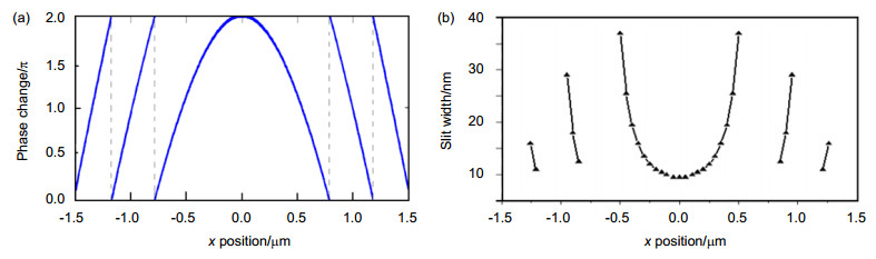
Figure 2. (a) Required phase change for the point-to-point imaging of an object localized on the axis x=0 as a function of x, which is the position of each nanoslit. (b) Distribution of widths and positions of nanoslits in the plasmofluidic lens.

Figure 3. (a) Dependence of the phase retardation on the slit width at three different wavelengths. The incident wavelengths are 730 nm, 810 nm and 920 nm. (b) Calculated phase retardations of the arrayed nanoslits in the plasmonic lens at three different wavelengths when the widths and positions of nanoslits are fixed. The blue curve represents the required phase change for the subwavelength imaging.
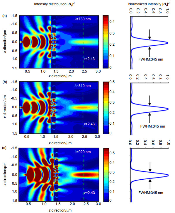
Figure 4. Calculated optical field distribution of the simulation result (left) and cross section of image plane at z=2.43 μm (right) is shown at wavelengths (a) 730 nm, (b) 810 nm and (c) 920 nm. The light source is localized at point x=0, z=0.3 μm, and the plasmonic lens ranges from z=1.3 μm to z=1.5 μm.
-
[1] Pendry J B. Negative refraction makes a perfect lens[J]. Physical Review Letters, 2000, 85: 3966-3969. doi: 10.1103/PhysRevLett.85.3966
[2] Ramakrishna S A, Pendry J B, Schurig D, et al. The asymmetric lossy near-perfect lens[J]. Journal of Modern Optics, 2002, 49(10): 1747-1762. doi: 10.1080/09500340110120950
[3] Fang N, Lee H, Sun Cheng, et al. Sub-diffraction-limited optical imaging with a silver superlens[J]. Science, 2005, 308(5721): 534-537. doi: 10.1126/science.1108759
[4] Lee H, Xiong Yi, Fang N, et al. Realization of optical superlens imaging below the diffraction limit[J]. New Journal of Physics, 2005, 7: 255. doi: 10.1088/1367-2630/7/1/255
[5] Zeng Beibei, Yang Xufeng, Wang Changtao, et al. Plasmonic interference nanolithography with a double-layer planar silver lens structure[J]. Optics Express, 2009, 17(19): 16783-16791. doi: 10.1364/OE.17.016783
[6] Durant S, Liu Zhaowei, Steele J M, et al. Theory of the trans-mission properties of an optical far-field superlens for imaging beyond the diffraction limit[J]. Journal of the Optical Society of America B, 2006, 23(11): 2383-2392. doi: 10.1364/JOSAB.23.002383
[7] Sun Zhijun, Kim H K. Refractive transmission of light and beam shaping with metallic nano-optic lenses[J]. Applied Physics Letters, 2004, 85(4): 642-644. doi: 10.1063/1.1776327
[8] Shi Haofei, Wang Changtao, Du Chunlei, et al. Beam manipulating by metallic nano-slits with variant widths[J]. Optics Express, 2005, 13(18): 6815-6820. doi: 10.1364/OPEX.13.006815
[9] Verslegers L, Catrysse P B, Yu Zhongfu, et al. Planar lenses based on nanoscale slit arrays in a metallic film[J]. Nano Letters, 2009, 9(1): 235-238. doi: 10.1021/nl802830y
[10] Xu Ting, Du Cunlei, Wang Changtao, et al. Subwavelength imaging by metallic slab lens with nanoslits[J]. Applied Physics Letters, 2007, 91(20): 201501. doi: 10.1063/1.2811711
[11] Ronchi V. Giovan Battista Amici's contribution to the advances of optical microscopy[J]. Physis; Rivista Internazionale di Storia Della Scienza, 1969, 11: 520-533.
[12] Wood R W. The mercury paraboloid as a reflecting telescope[J]. Astrophysical Journal, 1909, 29: 164-176. doi: 10.1086/141639
[13] Haas W E. Liquid crystal adiSplay research: the first fifteen years[J]. Molecular Crystals and Liquid Crystals, 1983, 94(2): 1-31.
[14] Mao Xiaole, Lin S C S, Lapsley M I, et al. Tunable liquid gradient refractive index (L-GRIN) lens with two degrees of freedom[J]. Lab on a Chip, 2009, 9(14): 2050-2058. doi: 10.1039/b822982a
[15] Psaltis D, Quake S R, Yang C. Developing optofluidic technology through the fusion of microfluidics and optics[J]. Nature, 2006, 442(7101): 381-386. doi: 10.1038/nature05060
[16] Gay G, Alloschery O, Weiner J, et al. Surface quality and surface waves on subwavelength-structured silver films[J]. Physical Review E, 2007, 75(1): 016612. doi: 10.1103/PhysRevE.75.016612
[17] Lalanne P, Hugonin J P, Rodier J C. Theory of surface Plasmon generation at nanoslit apertures[J]. Physical Review Letters, 2005, 95(26): 263902. doi: 10.1103/PhysRevLett.95.263902
[18] Xu Ting, Wu Y K, Luo Xiangang, et al. Plasmonic nanoresonators for high-resolution colour filtering and spectral imaging[J]. Nature Communications, 2010, 1(5): 59.
[19] Fu Yongqi, Zhou W, Lim L E N, et al. Plasmonic microzone plate: superfocusing at visible regime[J]. Applied Physics Letters, 2007, 91(6): 061124. doi: 10.1063/1.2769942
[20] Zhao Yanhui, Lin S C S, Nawaz A A, et al. Beam bending via plasmonic lenses[J]. Optics Express, 2010, 18(22): 23458- 23465. doi: 10.1364/OE.18.023458
[21] Xu Ting, Zhao Yanhui, Gan Dachun, et al. Directional excitation of surface plasmons with subwavelength slits[J]. Applied Physics Letters, 2008, 92(10): 101501. doi: 10.1063/1.2894183
[22] Weber M J. Handbook of Optical Materials[M]. Boston, USA: CRC, 2003.
[23] Gordon R, Brolo A G. Increased cut-off wavelength for a subwavelength hole in a real metal[J]. Optics Express, 2005, 13(6): 1933-1938. doi: 10.1364/OPEX.13.001933
[24] Zeng Beibei, Yang Xuefeng, Wang Changtao, et al. Su-per-resolution imaging at different wavelengths by using a one-dimensional metamaterial structure[J]. Journal of Optics, 2010, 12(3): 035104. doi: 10.1088/2040-8978/12/3/035104
[25] Luo Xiangang, Ishihara T. Surface plasmon resonant interference nanolithography technique[J]. Applied Physics Letters, 2004, 84(23): 4780-4782. doi: 10.1063/1.1760221
[26] Zeng Beibei, Pan Li, Liu Ling, et al. Improved near field lithography by surface plasmon resonance in groove-patterned masks[J]. Journal of Optics A: Pure and Applied Optics, 2009, 11(12): 125003. doi: 10.1088/1464-4258/11/12/125003
-
 下载:
下载:
 点击扫一扫
点击扫一扫
图(4)
计量
- 文章访问数: 6013
- PDF下载数: 2357
- 施引文献: 0


