
 E-mail Alert
 RSS
RSS
| Citation: |
Jiao Lin, Dapeng Wang, Guangyuan Si. Recent progress on plasmonic metasurfaces[J]. Opto-Electronic Engineering, 2017, 44(3): 289-296. doi: 10.3969/j.issn.1003-501X.2017.03.003

|
Recent progress on plasmonic metasurfaces
-
Abstract
Conventional optical systems (lenses, wave-plates and holograms) shape the wavefront of light within the range of an optical path that is much larger than the wavelength of light. The control of amplitude, phase and polarization of light depends on the dynamic optical path difference accumulated through the reflection, refraction and diffraction. Recently, planar ultrathin optical components have attracted tremendous attention by removing such traditional limitations. In this paper, we mainly review the recent progress of plasmonic metasurfaces with respect to wavefront shaping of free space and localized optical fields, including the fundamental mechanisms and applications. Both the drawbacks of existing technology and potential development are highlighted.-
Keywords:
- surface plasmon polaritons /
- metasurfaces /
- wavefront shaping
-

-
References
[1] Chen P Y, Soric J, Alù A. Invisibility and cloaking based on scattering cancellation[J].Advanced Materials, 2012, 24(44): OP281-OP304. [2] Ni Xingjie, Wong Zijing, Mrejen M, et al. An ultrathin invisibility skin cloak for visible light[J]. Science, 2015, 349(6254): 1310- 1314. doi: 10.1126/science.aac9411 [3] Liu Wei, Zhang Jianfa, Lei Bing, et al. Invisible nanowires with interfering electric and toroidal dipoles[J]. Optics Letters, 2015, 40(10): 2293-2296. doi: 10.1364/OL.40.002293 [4] Valentine J, Zhang Shuang, Zentgraf T, et al. Three-dimensional optical metamaterial with a negative refractive index[J]. Nature, 2008, 455(7211): 376-379. doi: 10.1038/nature07247 [5] Pendry J B. Negative refraction makes a perfect lens[J]. Physical Review Letters, 2000, 85(18): 3966-3969. doi: 10.1103/PhysRevLett.85.3966 [6] Wu Aimin, Li Hao, Du Junjie, et al. Experimental demonstration of in-plane negative-angle refraction with an array of silicon nanoposts[J]. Nano Letters, 2015, 15(3): 2055-2060. doi: 10.1021/nl5049516 [7] Shalaev V. Optical negative-index metamaterials[J]. Nature Photonics, 2007, 1(1): 41-48. doi: 10.1038/nphoton.2006.49 [8] Genov D A, Zhang Shuang, Zhang Xiang. Mimicking celestial mechanics in metamaterials[J].Nature Physics, 2009, 5(9): 687-692. doi: 10.1038/nphys1338 [9] Echtermeyer T J, Milana S, Sassi U, et al. Surface plasmon polariton graphene photodetectors[J]. Nano Letters, 2016, 16(1): 8-20. doi: 10.1021/acs.nanolett.5b02051 [10] Demetriadou A, Kornyshev A A. Principles of nanoparticle imaging using surface plasmons[J].New Journal of Physics, 2015, 17: 013041. doi: 10.1088/1367-2630/17/1/013041 [11] Alizadeh M H, Reinhard B M. Enhanced optical chirality through locally excited surface plasmon polaritons[J]. ACS Photonics, 2015, 2(7): 942-949. doi: 10.1021/acsphotonics.5b00151 [12] Zhang Haochi, Fan Yifeng, Guo Jian, et al. Second-harmonic generation of spoof surface plasmon polaritons using nonlinear plasmonic metamaterials[J]. ACS Photonics, 2016, 3(1): 139- 146. doi: 10.1021/acsphotonics.5b00580 [13] Ebbesen T W, Lezec H J, Ghaemi H F, et al. Extraordinary optical transmission through sub-wavelength hole arrays[J]. Nature, 1998, 391(6668): 667-669. doi: 10.1038/35570 [14] Weiner J. The physics of light transmission through subwavelength apertures and aperture arrays[J]. Reports on Progress in Physics, 2009, 72(6): 064401. doi: 10.1088/0034-4885/72/6/064401 [15] Johns P, Yu Kuai, Devadas M S, et al. Role of resonances in the transmission of surface plasmon polaritons between nanostructures[J]. ACS Nano, 2016, 10(3): 3375-3381. doi: 10.1021/acsnano.5b07185 [16] Wang Qianjin, Li Jiaqi, Huang Chengping, et al. Enhanced optical transmission through metal films with rotation- symmetrical hole arrays[J]. Applied Physics Letters, 2005, 87(9): 091105. doi: 10.1063/1.2034120 [17] Glybovski S B, Tretyakov S A, Belov P A, et al. Metasurfaces: from microwaves to visible[J]. Physics Reports, 2016, 634: 1-72. doi: 10.1016/j.physrep.2016.04.004 [18] Zhao Yang, Alù A. Tailoring the dispersion of plasmonic nanorods to realize broadband optical meta-waveplates[J]. Nano Letters, 2013, 13(3): 1086-1091. doi: 10.1021/nl304392b [19] Jiang Zhihao, Lin Lan, Ma Ding, et al. Broadband and wide field-of-view plasmonic metasurface-enabled waveplates[J]. Scientific Reports, 2014, 4: 7511. [20] Jahani S, Jacob Z. All-dielectric metamaterials[J]. Nature Nanotechnology, 2016, 11(1): 23-36. doi: 10.1038/nnano.2015.304 [21] Yang Yuanmu, Kravchenko I I, Briggs D P, et al. All-dielectric metasurface analogue of electromagnetically induced transparency[J]. Nature Communications, 2014, 5: 5753. doi: 10.1038/ncomms6753 [22] Paniagua-Domínguez R, Yu Yefeng, Miroshnichenko A E, et al. Generalized brewster effect in dielectric metasurfaces[J]. Nature Communications, 2016, 7: 10362. doi: 10.1038/ncomms10362 [23] Dai Yanmeng, Ren Wenzhen, Cai Hongbing, et al. Realizing full visible spectrum metamaterial half-wave plates with patterned metal nanoarray/insulator/metal film structure[J]. Optics Express, 2014, 22(7): 7465-7472. doi: 10.1364/OE.22.007465 [24] Pors A, Nielsen M G, Bozhevolnyi S I. Broadband plasmonic half-wave plates in reflection[J]. Optics Letters, 2013, 38(4): 513-515. doi: 10.1364/OL.38.000513 [25] Yu Nanfang, Genevet P, Kats M A, et al. Light propagation with phase discontinuities: generalized laws of reflection and refraction[J]. Science, 2011, 334(6054): 333-337. doi: 10.1126/science.1210713 [26] Gorodetski Y, Niv A, Kleiner V, et al. Observation of the spin-based plasmonic effect in nanoscale structures[J]. Physical Review Letters, 2008, 101(4): 043903. doi: 10.1103/PhysRevLett.101.043903 [27] Bliokh K Y, Gorodetski Y, Kleiner V, et al. Coriolis effect in optics: unified geometric phase and spin-hall effect[J]. Physical Review Letters, 2008, 101(3): 030404. doi: 10.1103/PhysRevLett.101.030404 [28] Shitrit N, Bretner I, Gorodetski Y, et al. Optical spin hall effects in plasmonic chains[J]. Nano Letters, 2011, 11(5): 2038-2042. doi: 10.1021/nl2004835 [29] Gorodetski Y, Shitrit N, Bretner I, et al. Observation of optical spin symmetry breaking in nanoapertures[J]. Nano Letters, 2009, 9(8): 3016-3019. doi: 10.1021/nl901437d [30] Lin Jiao, Genevet P, Kats M A, et al. Nanostructured holograms for broadband manipulation of vector beams[J]. Nano Letters, 2013, 13(9): 4269-4274. doi: 10.1021/nl402039y [31] Tan P S, Yuan X C, Lin J, et al. Surface plasmon polaritons generated by optical vortex beams[J]. Applied Physics Letters, 2008, 92(11): 111108. doi: 10.1063/1.2890058 [32] Tan P S, Yuan X C, Lin J, et al. Analysis of surface plasmon interference pattern formed by optical vortex beams[J]. Optics Express, 2008, 16(22): 18451-18456. doi: 10.1364/OE.16.018451 [33] Zhan Qiwen. Cylindrical vector beams: from mathematical concepts to applications[J].Advances in Optics and Photonics, 2009, 1(1): 1-57. doi: 10.1364/AOP.1.000001 [34] Willner A E, Huang F, Yan Y, et al. Optical communications using orbital angular momentum beams[J]. Advances in Optics and Photonics, 2015, 7(1): 66-106. doi: 10.1364/AOP.7.000066 [35] Genevet P, Lin Jiao, Kats M A, et al. Holographic detection of the orbital angular momentum of light with plasmonic photodiodes[J]. Nature Communications, 2012, 3: 1278. doi: 10.1038/ncomms2293 [36] Du Luping, Kou Shanshan, Balaur E, et al. Broadband chirality-coded meta-aperture for photon-spin resolving[J]. Nature Communications, 2015, 6: 10051. doi: 10.1038/ncomms10051 [37] Wang Xiaoli, Tang Zhiyong. Circular dichroism studies on plasmonic nanostructures[J].Small, 2017, 13(1): 1601115. doi: 10.1002/smll.v13.1 [38] Deng Haidong, Chen Xingyu, Xu Yi, et al. Single protein sensing with asymmetric plasmonic hexamer via fano resonance enhanced two-photon luminescence[J]. Nanoscale, 2015, 7(48): 20405-20413. doi: 10.1039/C5NR04118J [39] Neugebauer M, Woźniak P, Bag A, et al. Polarization-controlled directional scattering for nanoscopic position sensing[J]. Nature Communications, 2016, 7: 11286. doi: 10.1038/ncomms11286 [40] Wei Shibiao, Lei Ting, Du Luping, et al. Sub-100nm resolution PSIM by utilizing modified optical vortices with fractional topological charges for precise phase shifting[J]. Optics Express, 2015, 23(23): 30143-30148. doi: 10.1364/OE.23.030143 [41] Liu Zhaowei, Wei Qihuo, Zhang Xiang. Surface plasmon interference nanolithography[J].Nano Letters, 2005, 5(5): 957- 961. doi: 10.1021/nl0506094 [42] Tame M S, McEnery K R, Özdemir Ş K, et al. Quantum plasmonics[J]. Nature Physics, 2013, 9(6): 329-340. doi: 10.1038/nphys2615 [43] Tetienne J P, Lombard A, Simpson D A, et al. Scanning nanospin ensemble microscope for nanoscale magnetic and thermal imaging[J]. Nano Letters, 2016, 16(1): 326-333. doi: 10.1021/acs.nanolett.5b03877 [44] Ciraci C, Hill R T, Mock J J, et al. Probing the ultimate limits of plasmonic enhancement[J]. Science, 2012, 337(6098): 1072- 1074. doi: 10.1126/science.1224823 [45] Ye Jian, Wen Fangfang, Sobhani H, et al. Plasmonic nanoclusters: near field properties of the fano resonance interrogated with SERS[J]. Nano Letters, 2012, 12(3): 1660- 1667. doi: 10.1021/nl3000453 [46] Urban M J, Zhou Chao, Duan Xiaoyang, et al. Optically resolving the dynamic walking of a plasmonic walker couple[J]. Nano Letters, 2015, 15(12): 8392-8396. doi: 10.1021/acs.nanolett.5b04270 [47] Mühlenbernd H, Georgi P, Pholchai N, et al. Amplitude- and phase-controlled surface plasmon polariton excitation with metasurfaces[J]. ACS Photonics, 2016, 3(1): 124-129. doi: 10.1021/acsphotonics.5b00536 [48] O'Connor D, Ginzburg P, Rodríguez-Fortuño F J, et al. Spin-orbit coupling in surface plasmon scattering by nanostructures[J]. Nature Communications, 2014, 5: 5327. doi: 10.1038/ncomms6327 [49] Gubbin C R, Martini F, Politi A, et al. Strong and coherent coupling between localized and propagating phonon polaritons[J]. Physical Review Letters, 2016, 116(24): 246402. doi: 10.1103/PhysRevLett.116.246402 [50] Xu Ting, Wang Changtao, Du Chunlei, et al. Plasmonic beam deflector[J]. Optics Express, 2008, 16(7): 4753-4759. doi: 10.1364/OE.16.004753 [51] 赵泽宇, 蒲明博, 王彦钦, 等.广义折反射定律[J].光电工程, 2017, 44(2): 129-139. Zhao Zeyu, Pu Mingbo, Wang Yanqin, et al. The generalized laws of refraction and reflection[J].Opto-Electronic Engineering, 2017, 44(2): 129-139. [52] Chen Houtong, Taylor A J, Yu Nanfang. A review of metasurfaces: physics and applications[J]. Reports on Progress in Physics, 2016, 79(7): 076401. doi: 10.1088/0034-4885/79/7/076401 [53] Zhang Lei, Mei Shengtao, Huang Kun, et al. Advances in full control of electromagnetic waves with metasurfaces[J]. Advanced Optical Materials, 2016, 4(6): 818-833. doi: 10.1002/adom.v4.6 [54] Lin Jiao, Dellinger J, Genevet P, et al. Cosine-gauss plasmon beam: a localized long-range nondiffracting surface wave[J]. Physical Review Letters, 2012, 109(9): 093904. doi: 10.1103/PhysRevLett.109.093904 [55] Wei Shibiao, Lin Jiao, Wang Qian, et al. Singular diffraction-free surface plasmon beams generated by overlapping phase-shifted sources[J]. Optics Letters, 2013, 38(7): 1182-1184. doi: 10.1364/OL.38.001182 [56] Wei Shibiao, Lin Jiao, Wang Rong, et al. Self-imaging generation of plasmonic void arrays[J]. Optics Letters, 2013, 38(15): 2783-2785. doi: 10.1364/OL.38.002783 [57] López-Tejeira F, Rodrigo S G, Martín-Moreno L, et al. Efficient unidirectional nanoslit couplers for surface plasmons[J]. Nature Physics, 2007, 3(5): 324-328. doi: 10.1038/nphys584 [58] Baron A, Devaux E, Rodier J C, et al. Compact antenna for efficient and unidirectional launching and decoupling of surface plasmons[J]. Nano Letters, 2011, 11(10): 4207-4212. doi: 10.1021/nl202135w [59] Lin Jiao, Mueller J P B, Wang Qian, et al. Polarization-controlled tunable directional coupling of surface plasmon polaritons[J]. Science, 2013, 340(6130): 331-334. doi: 10.1126/science.1233746 [60] Lin Jiao, Wang Qian, Yuan Guanghui, et al. Mode-matching metasurfaces: coherent reconstruction and multiplexing of surface waves[J]. Scientific Reports, 2015, 5(1): 10529. [61] Kou Shanshan, Yuan Guanghui, Wang Qian, et al. On-chip photonic fourier transform with surface plasmon polaritons[J]. Light: Science & Applications, 2016, 5: e16034. -
Overview

Abstract:Organic light emitting devices (OLEDs) have some performances, such as low power consumption, ultra-light, fast response speed, high-definition, self-luminous and viewing angle, etc, which are expected to become a mainstream of the next generation of display devices. It is found that the microcavity structure can narrow the luminescence spectrum of the thin film and improve the luminescence color purity of the device effectively. We prepared a light-emitting device by using high vacuum deposition process and high-precision film thickness detector. This paper designed and prepared the green OLED devices based on double metallic mirrors in microcavity structures, of which the process was by vacuum evaporation and double metallic mirrors of devices: Al/MO3 as device of anode and hole injection layer, and LiF/Al as device cathode and electron injection layers. Organic material C545T was as green microcavity device of light-emitting materials. The device structure is Al(20 nm)/MoO3(4 nm)/2T-NATA(10 nm)/NPB(15 nm)/NPB:C545T(x%, 20 nm)/Alq3: C545T (4%, 20 nm)/Bphen (35 nm)/LiF(1 nm)/Al(200 nm), where x is the doping concentration, denoted as device B1. In order to analyze the microcavity effect, another preparation was made based on the ITO reference device B2. The microcavity effect of the device was analyzed by comparing the device's luminous brightness, luminous efficiency and luminescent color purity. The experimental results show that the device has the best optical and electrical properties when the doping concentration of device B1 is 3%. We found B1 and B2 color coordinates, (0.289, 0.620) and (0.317, 0.557), respectively. It can be judged that the luminescent color of the microcavity device B1 is purer. Then, microcavity device for microcavity effects could improve forward direction luminance intensity and luminance efficiency. At 100 mA/cm2, the brightness of devices B1 and B2 are 5076 cd/m2and 4818 cd/m2, and the maximum brightness of the both devices are 9277.7 cd/m2 and 10440 cd/m2. At 100 mA/cm2, luminance efficiencies of devices B1 and B2 are 6.0 cd/A and 5.61 cd/A, and the maximum luminance efficiencies of the both devices were 8.6 cd/A and 7.97 cd/A. We can conclude that, compared with the reference device, the green microcavity device has better luminous efficiency and color purity than the reference device under the effect of the microcavity, and the photoelectric performance of the device is best when the C545T doping concentration is 3% and the thickness is 20 nm.
-
Access History


Export File
Citation
Jiao Lin, Dapeng Wang, Guangyuan Si. Recent progress on plasmonic metasurfaces[J]. Opto-Electronic Engineering, 2017, 44(3): 289-296. doi: 10.3969/j.issn.1003-501X.2017.03.003
Format
Content
 DownLoad:


-
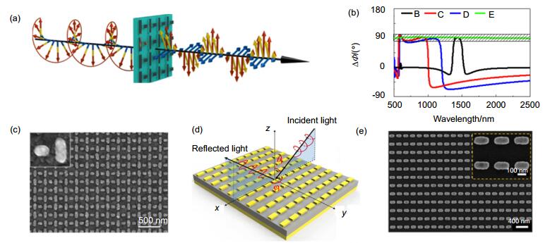
Figure 1.
(a) Schematic of quarter waveplate achieved by T-type nanoantennas [18]. (b) Phase shift of orthogonal linearly polarization light as a function of wavelength [18]. The B-line represents the structural parameters of lx=160 nm, ly=160 nm and z=8 nm. The C-line represents the structural parameters of lx=60 nm, ly=160 nm and z=45 nm. The D-line represents the structural parameters of lx=60 nm, ly=240 nm and z=50 nm. The E-line represents the structural parameters of lx=10 nm, ly=160 nm and z=60 nm. The width of nanoantenna is 20 nm and the gap is 10 nm. (c) Scanning electron microscope (SEM) images of interleaved nanoantennas [18]. (d) Schematic of metal-insulator-metal (MIM) reflective metasurfaces with broadband angles [19]. (e) SEM images of the typical unit cells in (d). The overview scale bar is 400 nm and the inserted scale bar is 100 nm [19].
-
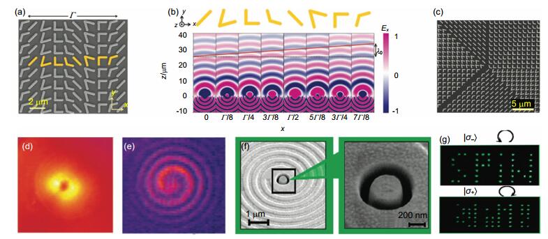
Figure 2.
(a) Scanning electron microscope (SEM) images of Ⅴ-antenna array [25]. (b) The representative Ⅴ-antenna nanostructures corresponding to eight discretized phase difference [25]. (c) SEM images of a plasmonic interface that creates an optical vortex [25]. (d) The measured far-field intensity distribution of an optical vortex with topological charge one [25]. (e) The measured spiral pattern created by the interference of vortex beam and co-propagating Gaussian beam [29]. (f) The magnified SEM image of spiral corrugations of spin-dependent transmission [29]. (g) The differently measured light transmissions for |σ-〉 and |σ+〉 illuminations [29].
-
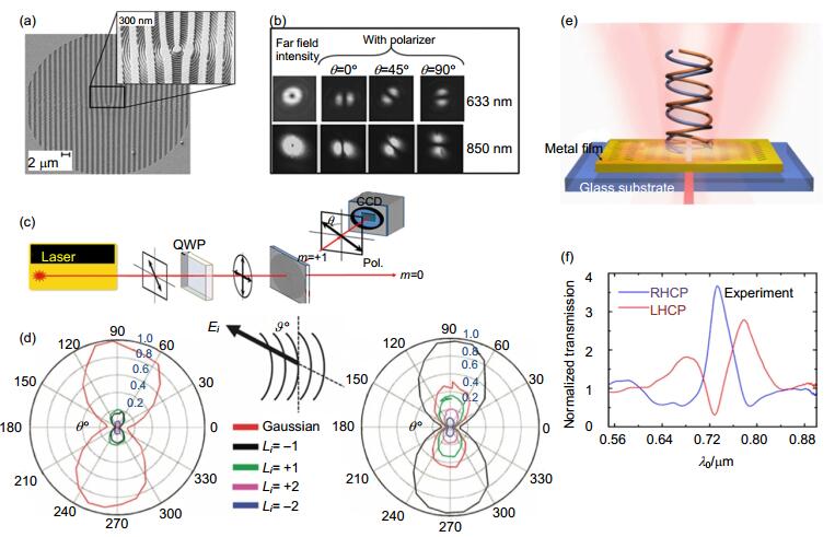
Figure 3.
(a) The fabricated structure for generating a radially polarized beam [30]. (b) The measured far-field intensity distributions at the wavelengths of 633 nm and 850 nm [30]. (c) The experimental setup [30]. (d) Detected photocurrent as functions of incident polarization and orbit angular momentum [35]. (e) Schematic of chiral meta-aperture [36]. (f) The measured transmission spectra for both left and right handed circularly polarized light [36].
-
Figure 4.
(a) The near-field intensity distribution of localized Cosine-Gaussian beam observed by a near-field scanning optical microscope. The propagating length is 80 μm [55]. (b) The plasmonic voids achieved by interleaved metal gratings. Talbot effect is observed [56].
-
Figure 5.
(a) The experimental result of unidirectional nanoslit coupler for surface plasmons [57]. (b) The numerical simulation of compact antenna for unidirectional launching and decoupling of surface plasmons [58]. (c) Schematic of polarization-controllable tunable directional coupling metasurfaces [59]. (d), (e) Near-field scanning optical microscope image of the metasurface under chiral illuminations [59].
-
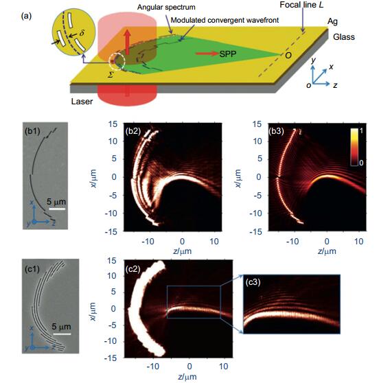
Figure 6.
(a) Schematic of in-plane Fourier transform for generating a converging SPP [61]. (b1)~(b3) represent the fabricated structures of scanning electron microscope (SEM) image, intensity distribution observed by a near-field scanning optical microscope (NSOM) and numerical simulation of plasmoic Weber beam, respectively [61]. (c1)~(c3) represent the fabricated structures of plasmonic Airy beam generator, the NSOM measurement result and zoom-in view of blue box, respectively [61].


