
 E-mail Alert
 RSS
RSS
| Citation: |
Xu Kaichen, Zhang Chentao, Lu Tzu Hsiao, et al. Hybrid metal‐insulator‐metal structures on Si nanowires array for surface enhanced Raman scattering[J]. Opto-Electronic Engineering, 2017, 44(2): 185-191. doi: 10.3969/j.issn.1003-501X.2017.02.006

|
Hybrid metal‐insulator‐metal structures on Si nanowires array for surface enhanced Raman scattering
-
Abstract
Surface enhanced Raman scattering (SERS) is an efficient technique to detect low concentration molecules. In this work, periodical silicon nanowires (SiNWs) integrated with metal-insulator-metal (MIM) layers are employed as SERS substrates. Laser interference lithography (LIL) combined with reactive ion etching (RIE) is used to fabricate large-area periodic nanostructures, followed by decorating the MIM layers. Compared to MIM disks array on Si surface, the SERS enhancement factor (EF) of the MIM structures on the SiNWs array can be increased up to 5 times, which is attributed to the enhanced electric field at the boundary of the MIM disks. Furthermore, high density of nanoparticles and nanogaps serving as hot spots on sidewall surfaces also contribute to the enhanced SERS signals. Via changing the thickness of the insulator layer, the plasmonic resonance can be tuned, which provides a new localized surface plasmon resonance (LSPR) characteristic for SERS applications.
-

-
References
[1] Kneipp K, Wang Yang, Kneipp H, et al. Single molecule detection using surface-enhanced Raman scattering (SERS)[J]. Physical Review Letters, 1997, 78(9): 1667-1670. doi: 10.1103/PhysRevLett.78.1667 [2] Campion A, Kambhampati P. Surface-enhanced Raman scattering[J]. Chemical Society Reviews, 1998, 27(4): 241-250. doi: 10.1039/a827241z [3] Quyen T T B, Chang C C, Su W N, et al. Self-focusing Au@SiO2 nanorods with rhodamine 6G as highly sensitive SERS substrate for carcinoembryonic antigen detection[J]. Journal of Materials Chemistry B, 2014, 2(6): 629-636. doi: 10.1039/C3TB21278E [4] Wang Yan, Zhang Xiujuan, Gao Peng, et al. Air heating approach for multilayer etching and roll-to-roll transfer of silicon nanowire arrays as SERS substrates for high sensitivity molecule detection[J]. ACS Applied Materials & Interfaces, 2014, 6(2): 977-984. [5] Xu Kaichen, Zhang Chentao, Zhou Rui, et al. Hybrid micro/nano-structure formation by angular laser texturing of Si surface for surface enhanced Raman scattering[J]. Optics Express, 2016, 24(10): 10352-10358. doi: 10.1364/OE.24.010352 [6] Indrasekara A S D S, Meyers S, Shubeita S, et al. Gold nanostar substrates for SERS-based chemical sensing in the femtomolar regime[J]. Nanoscale, 2014, 6(15): 8891-8899. doi: 10.1039/C4NR02513J [7] Dmitriev A, Hägglund C, Chen Si, et al. Enhanced nanoplasmonic optical sensors with reduced substrate effect[J]. Nano Letters, 2008, 8(11): 3893-3898. doi: 10.1021/nl8023142 [8] Chirumamilla M, Toma A, Gopalakrishnan A, et al. 3D nanostar dimers with a sub-10-nm gap for single-/few-molecule surface-enhanced Raman scattering[J]. Advanced Materials, 2014, 26(15): 2353-2358. doi: 10.1002/adma.v26.15 [9] Hatab N A, Hsueh C H, Gaddis A L, et al. Free-standing optical gold bowtie nanoantenna with variable gap size for enhanced Raman spectroscopy[J]. Nano Letters, 2010, 10(12): 4952- 4955. doi: 10.1021/nl102963g [10] Ding Li, Qin Jin, Guo Songpo, et al. Resonant effects in nano scale bowtie apertures[J]. Scientific Reports, 2016, 6: 27254. doi: 10.1038/srep27254 [11] Yan Zhendong, Du Wei, Tu Linlin, et al. A facile high-perfor mance SERS substrate based on broadband near-perfect optical absorption[J]. Journal of Raman Spectroscopy, 2015, 46(9): 795-801. doi: 10.1002/jrs.4721 [12] Cinel N A, Bütün S, Ertaş G, et al. 'Fairy chimney'-shaped tandem metamaterials as double resonance SERS substrates[J]. Small, 2013, 9(4): 531-537. doi: 10.1002/smll.v9.4 [13] Chu Yizhuo, Banaee M G, Crozier K B. Double-resonance plasmon substrates for surface-enhanced Raman scattering with enhancement at excitation and stokes frequencies[J]. ACS Nano, 2010, 4(5): 2804-2810. doi: 10.1021/nn901826q [14] Wells S M, Merkulov I A, Kravchenko I I, et al. Silicon nanopillars for field-enhanced surface spectroscopy[J]. ACS Nano, 2012, 6(4): 2948-2959. doi: 10.1021/nn204110z [15] Li Wendi, Ding Fei, Hu J, et al. Three-dimensional cavity nanoantenna coupled plasmonic nanodots for ultrahigh and uniform surface-enhanced Raman scattering over large area[J]. Optics Express, 2011, 19(5): 3925-3936. doi: 10.1364/OE.19.003925 [16] Polemi A, Wells S M, Lavrik N V, et al. Local field enhancement of pillar nanosurfaces for SERS[J]. The Journal of Physical Chemistry C, 2010, 114(42): 18096-18102. doi: 10.1021/jp106540q [17] Yang J, Li J B, Gong Q H, et al. High aspect ratio SiNW arrays with Ag nanoparticles decoration for strong SERS detection[J]. Nanotechnology, 2014, 25(46): 465707. doi: 10.1088/0957-4484/25/46/465707 [18] Yang Jing, Luo Fangfang, Kao T S, et al. Design and fabrication of broadband ultralow reflectivity black Si surfaces by laser micro/nanoprocessing[J]. Light: Science & Applications, 2014, 3(7): e185. [19] Seo K, Borguet E. Potential-induced structural change in a self-assembled monolayer of 4-methylbenzenethiol on Au(111)[J]. The Journal of Physical Chemistry C, 2007, 111(17): 6335-6342. doi: 10.1021/jp064493r [20] Li Weiyang, Camargo P H C, Au L, et al. Etching and dimerization: a simple and versatile route to dimers of silver nanospheres with a range of sizes[J]. Angewandte Chemie International Edition, 2010, 49(1): 164-168. doi: 10.1002/anie.200905245 [21] Cai W B, Ren B, Li X Q, et al. Investigation of surface-enhanced Raman scattering from platinum electrodes using a confocal Raman microscope: dependence of surface roughening pretreatment[J]. Surface Science, 1998, 406(1-3): 9-22. doi: 10.1016/S0039-6028(97)01030-3 [22] Toussaint K C, Jr, Roxworthy B J, Michaud S, et al. Plasmonic nanoantennas: from nanotweezers to plasmonic photography[J]. Optics and Photonics News, 2014, 26(6): 24-31. [23] Lévêque G, Martin O J F. Tunable composite nanoparticle for plasmonics[J]. Optics Letters, 2006, 31(18): 2750-2752. doi: 10.1364/OL.31.002750 [24] Liu C H, Hong M H, Cheung H W, et al. Bimetallic structure fabricated by laser interference lithography for tuning surface plasmon resonance[J]. Optics Express, 2008, 16(14): 10701-10709. doi: 10.1364/OE.16.010701 [25] Zhang Weihua, Ding Fei, Chou S Y. Large enhancement of upconversion luminescence of NaYF4: Yb3+/Er3+ nanocrystal by 3D plasmonic nano-antennas[J]. Advanced Materials, 2012, 24(35): OP236-OP241. -
Overview

Abstract: Surface enhanced Raman spectroscopy (SERS) has attracted a great amount of research interests in the past decades due to its fascinating use for finger-print molecules' detection. Two main mechanisms, chemical and electromagnetic enhancement, are used to explain the SERS phenomenon. In particular, the latter mechanism is widely accepted as the dominated effect. In recent years, a new kind of intriguing platform built from "elevated" cavity or bowtie arrays has been developed for reliable SERS detection. Known as the lightning-rod effect, bowtie nanoantenna arrays are able to confine the optical radiation into nanoscale volumes, performing excellent field concentration, which can exhibit distinct SERS effect due to strong LSP resonance in the vicinity of sharp nanotips of nanoparticles and small gaps among neighboring nanoparticles. The "elevated" properties make the cavity or bowtie decouple from the substrate, which is expected to enhance near-field intensity. However, such "elevated" nanocavity array is limited to the weak tunability of plamonic resonance and complicated fabrication processes, such as electron-beam lithography (EBL) and focused ion beam (FIB) milling. Their main disadvantages of high cost and slow throughput are not practical for SERS applications. In this work, periodical silicon nanowires (SiNWs) integrated with metal-insulator-metal (MIM) layers are employed as SERS substrates. Laser interference lithography (LIL) combined with reactive ion etching (RIE) is used to fabricate large-area periodic nanostructures, followed by decorating the MIM layers. Compared to MIM disks array on Si surface, the SERS enhancement factor (EF) of the MIM structures on the SiNWs array can be increased up to 5 times, which is attributed to the enhanced electric field at the boundary of the MIM disks. Furthermore, high density of nanoparticles and nanogaps serving as hot spots on sidewall surfaces also contribute to the enhanced SERS signals. Meanwhile, SiNWs array boosts the adsorption of probing molecules within the detection volume and light scattering within the SiNWs. It is also found that the calculated electric field enhancement demonstrates a periodic variation of pillar height, which is due to the constructive or destructive interference between the incident and reflected light. Via changing the thickness of the insulator layer, the plasmonic resonance can be tuned. These factors contribute to the enhanced SERS signals. This 3D platform with large area, good periodicity and pillar height dependent electric field enhancement can provide guidance for further optimizing and engineering such "elevated" plasmonic nanostructures for practical SERS applications.
-
Access History


Export File
Citation
Xu Kaichen, Zhang Chentao, Lu Tzu Hsiao, et al. Hybrid metal‐insulator‐metal structures on Si nanowires array for surface enhanced Raman scattering[J]. Opto-Electronic Engineering, 2017, 44(2): 185-191. doi: 10.3969/j.issn.1003-501X.2017.02.006
Format
Content
 DownLoad:


-
Figure 1.
Schematic of the fabrication procedures of MIM disks on SiNWs array by laser interference lithography and reactive ion etching.
-
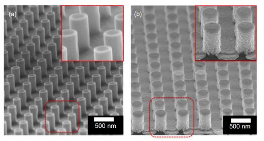
Figure 2.
SEM images (tilt-view 70°) of the fabricated (a) SiNWs array and (b) MIM disks on SiNWs array. The figures in the top right corner of Figs. 2(a) and (b) show the corresponding selected areas.
-
Figure 3.
SERS spectra of 4-MBT molecules adsorbed on 50 nm thick Au film on Si surface, Au disks array on Si surface, MIM disks array on Si surface and MIM disks on SiNWs array. Thickness of Au disks is 50 nm and Au-SiO2-Au layers 25-20-25 nm. All the period is 500 nm and height of SiNWs is ~400 nm.
-
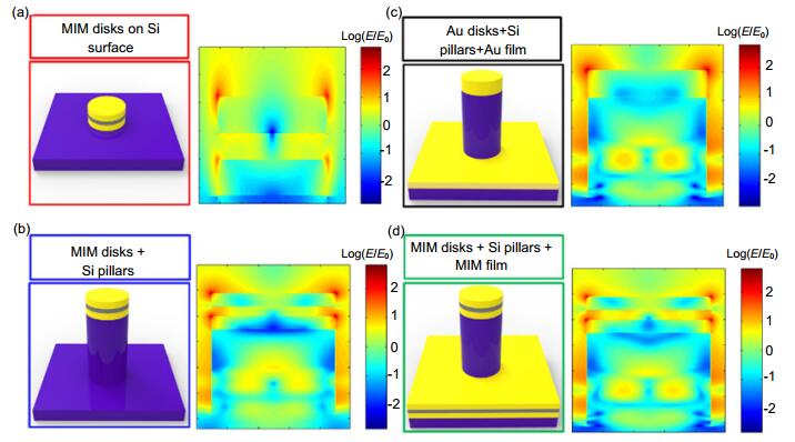
Figure 4.
Calculated electric field distribution (Log scale) at the excitation wavelength of 532 nm. (a) MIM disks array on Si surface. (b) MIM disks on SiNWs array without bottom metallic layers. (c) Only Au disks on SiNWs array with bottom metallic layers and (d) MIM disks on the SiNWs array with bottom MIM layers.
-
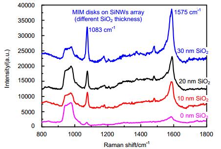
Figure 5.
SERS spectra of 4-MBT adsorbed on the MIM disks on SiNWs array at different thickness of SiO2 layer.
-
Figure S1.
(a) Sketch of a single hybrid structure, where thicknesses of Au-SiO2-Au layers are 25-20-25 nm with period of 500 nm, diameter of 200 nm and height of h. Point monitors 1 and 2 denote the simulated regions. (b) Calculated electric field enhancement (E/E0) at the excitation wavelength of 532 nm as a function of pillar height from 50 to 800 nm at a step of 50 nm.


