
 E-mail Alert
 RSS
RSS
| Citation: |
Asakawa K, Sugimoto Y, Nakamura S. Silicon photonics for telecom and data-com applications. Opto-Electron Adv 3, 200011 (2020). doi: 10.29026/oea.2020.200011

|
-
Abstract
In recent decades, silicon photonics has attracted much attention in telecom and data-com areas. Constituted of high refractive-index contrast waveguides on silicon-on-insulator (SOI), a variety of integrated photonic passive and active devices have been implemented supported by excellent optical properties of silicon in the mid-infrared spectrum. The main advantage of the silicon photonics is the ability to use complementary metal oxide semiconductor (CMOS) process-compatible fabrication technologies, resulting in high-volume production at low cost. On the other hand, explosively growing traffic in the telecom, data center and high-performance computer demands the data flow to have high speed, wide bandwidth, low cost, and high energy-efficiency, as well as the photonics and electronics to be integrated for ultra-fast data transfer in networks. In practical applications, silicon photonics started with optical interconnect transceivers in the data-com first, and has been now extended to innovative applications such as multi-port optical switches in the telecom network node and integrated optical phased arrays (OPAs) in light detection and ranging (LiDAR). This paper overviews the progresses of silicon photonics from four points reflecting the recent advances mentioned above. CMOS-based silicon photonic platform technologies, applications to optical transceiver in the data-com network, applications to multi-port optical switches in the telecom network and applications to OPA in LiDAR system. -

-
References
[1] Asahi Newspaper article (in Japanese), Jan 9, 2017. [2] History, NTT Network Innovation Laboratories. https://www.ntt.co.jp/mirai/e/history/. [3] Soref R, Bennett B. Electrooptical effects in silicon. IEEE J Quant Electron 23, 123-129 (1987). doi: 10.1109/JQE.1987.1073206 [4] Gunn G. CMOS Photonics for high-speed interconnects. IEEE Micro 26, 58-66 (2006). [5] Jalali B, Fathpour S. Silicon photonics. J Light Wave Technol 24, 4600-4615 (2006). doi: 10.1109/JLT.2006.885782 [6] Fang Z, Zhao C Z. Recent progress in silicon photonics: a review. ISRN Opt 2012, 428690 (2012). [7] Dhiman A. Silicon photonics: a review. IOSR J Appl Phys (IOSR-JAP) 3, 67-79 (2013). doi: 10.9790/4861-0356779 [8] Kumar A. Silicon photonics: An evolving technology. Int J Eng Sci Res Technol 5, 153-161 (2016). [9] Thomson D, Zilkie A, Bowers J E, Komljenovic T, Reed G T et al. Roadmap on silicon photonics. J Opt 18, 073003 (2016). doi: 10.1088/2040-8978/18/7/073003 [10] Bowers J E, Komljenovic T, Davenport M, Hulme J, Liu A Y et al. Recent advances in silicon photonic integrated circuits. Proc SPIE 9774, 977402 (2017). [11] Stojanović V, Ram R J, Popović M, Lin S, Moazeni S et al. Monolithic silicon-photonic platforms in state-of-the-art CMOS SOI processes[Invited]. Opt Express 26, 13106-13121 (2018). doi: 10.1364/OE.26.013106 [12] Hibino Y. Silica-based planar lightwave circuits and their applications. MRS Bull 28, 365-371 (2003). doi: 10.1557/mrs2003.102 [13] Bona G L, Germann R, Offrein B J. SiON high-refractive-index waveguide and planar lightwave circuits. IBM J Res Develop 47, 239-249 (2003). doi: 10.1147/rd.472.0239 [14] Vlasov Y A, McNab S J. Losses in single-mode silicon-on-insulator strip waveguides and bends. Opt Express 12, 1622-1631 (2004). doi: 10.1364/OPEX.12.001622 [15] Fang A W, Park H, Jones R, Cohen O, Paniccia M J et al. A continuous-wave hybrid AlGaInAs-silicon evanescent laser. IEEE Photon Technol Lett 18, 1143-1145 (2006). doi: 10.1109/LPT.2006.874690 [16] Pasquariello D, Hjort K. Plasma-assisted InP-to-Si low temperature wafer bonding. IEEE J Sel Top Quant Electron 8, 118-131 (2002). doi: 10.1109/2944.991407 [17] Lee A, Jiang Q, Tang M C, Seeds A, Liu H Y. Continuous-wave InAs/GaAs quantum-dot laser diodes monolithically grown on Si substrate with low threshold current densities. Opt Express 20, 22181-22187 (2012). doi: 10.1364/OE.20.022181 [18] Liu A Y, Zhang C, Norman J, Snyder A, Lubyshev D et al. High performance continuous wave 1.3 μm quantum dot lasers on silicon. Appl Phys Lett 104, 041104 (2014). doi: 10.1063/1.4863223 [19] Park H, Fang A W, Kodama S, Bowers J E. Hybrid silicon evanescent laser fabricated with a silicon waveguide and Ⅲ-V off set quantum wells. Opt Express 13, 9460-9464 (2005). doi: 10.1364/OPEX.13.009460 [20] Roelkens G, Van Thourhout D, Baets R, Nötzel R, Smit M. Laser emission and photodetection in an InP/InGaAsP layer integrated on and coupled to a silicon-on-insulator waveguide circuit. Opt Express 14, 8154-8159 (2006). doi: 10.1364/OE.14.008154 [21] Fang A W, Park H, Cohen O, Jones R, Paniccia M J et al.Electrically pumped hybrid AlGaInAs-silicon evanescent laser. Opt Express 14, 9203-9210 (2006). doi: 10.1364/OE.14.009203 [22] Liang D, Bowers J E. Recent progress in lasers on silicon. Nat Photon 4, 511-517 (2010). doi: 10.1038/nphoton.2010.167 [23] Maeda M W, Chang-Hasnain C, Von Lehmen A, Izadpanah H, Lin C et al. Multigigabit/s operations of 16-wavelength vertical-cavity surface-emitting laser array. IEEE Photon Technol Lett 3, 863-865 (1991). doi: 10.1109/68.93242 [24] Chang-Hasnain C J. Tunable VCSEL. IEEE J Sel Top Quantum Electron 6, 978-987 (2000). doi: 10.1109/2944.902146 [25] Kapon E, Sirbu A. Long-wavelength VCSELs: Power-efficient answer. Nat Photon 3, 27-29 (2009). doi: 10.1038/nphoton.2008.266 [26] Zhu L, Karagodsky V, Chang-Hasnain C J. Novel high efficiency vertical to in-plane optical coupler. Proc SPIE 8270, 82700L (2012). doi: 10.1117/12.909414 [27] Ferrara J, Yang W J, Zhu L, Qiao P F, Chang-Hasnain C J. Heterogeneously integrated long-wavelength VCSEL using silicon high contrast grating on an SOI substrate. Opt Express 23, 2512-2523 (2015). doi: 10.1364/OE.23.002512 [28] Akatsu T, Deguet C, Sanchez L, Allibert F, Rouchon D et al. Germanium-on-insulator (GeOI) substrates-A novel engineered substrate for future high performance devices. Mater Sci Semicond Proc 9, 444-448 (2006). doi: 10.1016/j.mssp.2006.08.077 [29] Tanoto H, Yoon S F, Lew K L, Loke W K, Dohrman C et al. Electroluminescence and structural characteristics of InAs/In0.1Ga0.9As quantum dots grown on graded Si1-xGex/Si substrate. Appl Phys Lett 95, 141905 (2009). doi: 10.1063/1.3243984 [30] Liu H Y, Wang T, Jiang Q, Hogg R, Tutu F et al. Long-wavelength InAs/GaAs quantum-dot laser diode monolithically grown on Ge substrate. Nat Photon 5, 416-419 (2011). doi: 10.1038/nphoton.2011.120 [31] Lee A, Jiang Q, Tang M C, Seeds A, Liu H Y. Continuous-wave InAs/GaAs quantum-dot laser diodes monolithically grown on Si substrate with low threshold current densities. Opt Express 20, 22181-22187 (2012). doi: 10.1364/OE.20.022181 [32] Seimetz M. Laser linewidth limitations for optical systems with high-order modulation employing feed forward digital carrier phase estimation. In Proceedings of Optical Fiber Communication Conference/National Fiber Optic Engineers Conference OTuM2 (OSA, 2008). [33] Komljenovic T, Srinivasan S, Norberg E, Davenport M, Fish G et al. Widely tunable narrow-linewidth monolithically integrated external-cavity semiconductor lasers. IEEE J Sel Top Quant Electron 21, 1501909 (2015). [34] Heck M J R, Bauters J F, Davenport, Doylend J K, Jain S et al. Hybird silicon photonic integrated circuit technology. IEEE J Sel Top Quant Electron 19, 6100117 (2013). doi: 10.1109/JSTQE.2012.2235413 [35] Xia F N, Sekaric L, Vlasov Y. Ultracompact optical buffers on a silicon chip. Nat Photon 1, 65-71 (2007). doi: 10.1038/nphoton.2006.42 [36] Srinivasan S, Davenport M, Komljenovic T, Hulme J, Spencer D T et al. Coupled-ring-resonator-mirror-based heterogeneous Ⅲ-V silicon tunable laser. IEEE Photon J 7, 2700908 (2015). [37] Stanton E J, Heck M J R, Bovington J, Spott A, Bowers J E. Multi-octave spectral beam combiner on ultra-broadband photonic integrated circuit platform. Opt Express 23, 11272-11283 (2015). doi: 10.1364/OE.23.011272 [38] Yaegashi H. Development of ultra-compact optical transceivers for IoT network utilizing silicon photonics technology. OKI Tech Rev 84, 1-4 (2017). [39] Little B E, Chu S T, Pan W, Kokubun Y. Microring resonator arrays for VLSI photonics. IEEE Photon Technol Lett 12, 323-325 (2000). doi: 10.1109/68.826928 [40] Xu Q F, Fattal D, Beausoleil R G. Silicon microring resonators with 1.5-μm radius. Opt Express 6, 4309-4315 (2008). [41] Silicon Photonics and Photonic Integrated Circuits 2020 report. Yole Développement (2020). https://s3.i-micronews.com/uploads/2020/04/YDR20088-Silicon-Photonics-Market-Technology-2020-Sample.pdf [42] Merritt R. Globalfoundries Cuts 5% of Workforce (2018-06-11). https://www.eetimes.com/globalfoundries-cuts-5-of-workforce/#. Original source by IC Insights [43] Intel labs. The 50G Silicon Photonics Link. http://download.intel.com/pressroom/pdf/photonics/50G_Silicon_Photonics_Link.pdf. [44] Soref R A, Lorenzo J P. Single-crystal silicon: a new material for 1.3 and 1.6 μm integrated-optical components. Electron Lett 21, 953-954 (1985). doi: 10.1049/el:19850673 [45] Reed G T, Headley W R, Png C E J. Silicon photonics: the early years. Proc SPIE 5730, 596921 (2005). [46] Rickman A. The commercialization of silicon photonics. Nat Photon 8, 579-582 (2014). doi: 10.1038/nphoton.2014.175 [47] Liu J F, Cannon D D, Wada K, Ishikawa Y, Jongthammanurak S et al. Tensile strained Ge p-i-n photodetectors on Si platform for C and L band telecommunications. Appl Phys Lett 87, 011110 (2005). doi: 10.1063/1.1993749 [48] Feng D, Luff B J, Jatar S, Asghari M. Micron-scale silicon photonic devices and circuits. In 2014 Optical Fiber Communications Conference (OFC) TH4C.1 (OSA, 2014); https://doi.org/10.1364/OFC.2014.Th4C.1. [49] Boeuf F, Cremer S, Temporiti E, Fere' M, Shaw M et al. Recent progress in silicon photonics R & D and manufacturing on 300mm wafer platform. In 2015 Optical Fiber Communications Conference (OFC) W3A.1 (OSA, 2015); https://doi.org/10.1364/OFC.2015.W3A.1. [50] Doerr C, Chen L, Vermeulen D, Nielsen T, Azemati S et al. Single-chip silicon photonics 100-Gb/s coherent transceiver. In 2014 Optical Fiber Communications Conference (OFC) Th5C.1 (OSA, 2014); https://doi.org/10.1364/OFC.2014.Th5C.1. [51] Silicon photonics shipments, for datacenter (In units) 2019-2025e. Yole Développement (2020). [52] Patterson D, De Sousa I, Achard L M. The future of packaging with silicon photonics. Chip Scale Rev, 1-10 (Jan, 2017). [53] Anthony S. IBM demos first fully integrated monolithic silicon photonics chip. Ars Technica UK (May, 2015). https://arstechnica.com/information-technology/2015/05/ibm-demos-first-fully-integrated-monolithic-silicon-photonics-chip/. [54] S. Narasimha, K. Onishi, H. M. Nayfeh, A. Waite, M. Weybright et al. High performance 45-nm SOI technology with enhanced strain, porous Low-k BEOL, and immersion lithography. In Proceedings of International Electron Devices Meeting, (IEEE, 2006), 1-4. [55] Orcutt J S, Moss B, Sun C, Leu J, Georgas M et al. Open foundry platform for high-performance electronic-photonic integration. Opt Express 20, 12222-12232 (2012). doi: 10.1364/OE.20.012222 [56] Sun C, Wade M, Georgas M, Lin S, Alloatti L et al. A 45 nm CMOS-SOI Monolithic photonics platform with bit-statistics-based resonant microring thermal tuning. IEEE J Solid-State Circuits 51, 893-907 (2016). doi: 10.1109/JSSC.2016.2519390 [57] Lee Y, Waterman A, Avizienis R, Cook H, Sun C et al. A 45nm 1.3GHz 16.7 double-precision GFLOPS/W RISC-V processor with vector accelerators. In ESSCIRC 2014-40th European Solid State Circuits Conference (ESSCIRC) 199-202 (IEEE, 2014); http://doi.org/10.1109/ESSCIRC.2014.6942056. [58] Akhter M S, Somogyi P, Sun C, Wade M, Meade R et al. Wavelight: a monolithic low latency silicon-photonics communication platform for the next-generation disaggregated cloud data centers. In 2017 IEEE 25th Symposium on High-Performance Interconnects (HOTI) 25-28 (IEEE, 2017); http://doi.org/10.1109/HOTI.2017.23. [59] Moazeni S, Lin S, Wade M T, Alloatti L, Ram R J et al. A 40Gb/s PAM-4 transmitter based on a ring-resonator optical DAC in 45nm SOI CMOS. IEEE J Solid-State Circuits 52, 3503-3516 (2017). doi: 10.1109/JSSC.2017.2748620 [60] Nakamura T, Yashiki K, Mizutani K, Nedachi T, Fujikata J et al. Fingertip-size optical module, "Optical I/O Core", and its application in FPGA. IEICE Trans Electron E102-C, 333-339 (2019). doi: 10.1587/transele.2018ODI0005 [61] http://www.aiocore.com/technology [62] Mogami T, Horikawa T, Kinoshita K, Hagihara Y, Ushida J et al. 1.2 Tbps/cm2 enabling silicon photonics IC technology based on 40-nm generation platform. J Lightw Technol 36, 4701-4712 (2018). doi: 10.1109/JLT.2018.2863779 [63] Uemura T, Ukita A, Takemura K, Kurihara M, Okamoto D et al. 125-μm-pitch×12-channel "Optical Pin" array as I/O structure for novel miniaturized optical transceiver chips. In 2015 IEEE 65th Electronic Components and Technology Conference (ECTC) (IEEE, 2015); http://doi.org/10.1109/ECTC.2015.7159766. [64] Yashiki K, Mizutani K, Ushida J, Suzuki Y, Kurihara M et al. 25-Gbps error-free operation of chip-scale Si-photonics optical transmitter over 70℃ with integrated quantum dot laser. In Optical Fiber Communications Conference and Exhibition (OFC) Th1F.7 (OSA, 2016). [65] https://www.corning.com/media/worldwide/coc/documents/Fiber/PI1468_07-14_English.pdf. [66] Cheng Q X, Bahadori M, Glick M, Rumley S, Bergman K. Recent advances in optical technologies for data centers: a review. Optica 5, 1354-1370 (2018). doi: 10.1364/OPTICA.5.001354 [67] Hinton H S. An Introduction to Photonic Switching Fabrics (Springer Science & Business Media, New York, 2013). [68] Tanizawa K, Suzuki K, Suda S, Matsuura H, Ikeda K et al. Silicon photonic 32×32 strictly-non-blocking blade switch and its full path characterization. In 2016 21st OptoElectronics and Communications Conference (OECC) held jointly with 2016 International Conference on Photonics in Switching (PS) (IEEE, 2016). https://ieeexplore.ieee.org/document/7718222. [69] Sakamaki Y, Kawai T, Fukutoku M. Next-generation optical switch technologies for realizing ROADM with more flexible functions. NTT Tech Rev 12, 1-5 (2014). [70] Basch E B, Egorov R, Gringeri S, Elby S. Architectural tradeoffs for reconfigurable dense wavelength-division multiplexing systems. IEEE J Sel Top Quant Electron 12, 615-626 (2006). doi: 10.1109/JSTQE.2006.876167 [71] Gringeri S, Basch B, Shukla V, Egorov R, Xia T J. Flexible architectures for optical transport nodes and networks. IEEE Commun Mag 48, 40-50 (2010). [72] https://www.cisco.com/c/dam/m/en_us/network-intelligence/service-provider/digital-transformation/knowledge-network-webinars/pdfs/1213-business-services-ckn.pdf. [73] Takeshita H, Hino T, Ishii K, Kurumida J.Prototype highly integrated 8×48 transponder aggregator based on Si photonics for multi-degree colorless, directionless, contentionless reconfigurable optical add/drop multiplexer. IEICE Trans Electron E96-C, 966-973 (2013). doi: 10.1587/transele.E96.C.966 [74] Yamazaki E, Yamanaka S, Kisaka Y, Nakagawa T, Murata K et al.Fast optical channel recovery in field demonstration of 100-Gbit/s Ethernet over OTN using real-time DSP. Opt Express 19, 13179-13184 (2011). doi: 10.1364/OE.19.013179 [75] Nakamura S, Yanagimachi S, Takeshita H, Tajima A, Hino T et al.Optical switches based on silicon photonics for ROADM application. IEEE J Sel Top Quant Electron 22, 3600609 (2016). [76] Nakamura S, Takahashi S, Ogura I, Ushida J, Kurata K et al.High extinction ratio optical switching independently of temperature with silicon photonic 1×8 switch. In Optical Fiber Communication Conference OTu2I.3 (OSA, 2012); https://doi.org/10.1364/OFC.2012.OTu2I.3. [77] Nakamura S, Yanagimachi S, Yanagimachi H, Tajima A, Kato T et al. Compact and low-loss 8×8 silicon photonic switch module for transponder aggregators in CDC-ROADM application. In Optical Fiber Communication Conference M2B.6 (OSA, 2015); https://doi.org/10.1364/OFC.2015.M2B.6. [78] Yanagimachi S, Nakamura S, Takeshita H, Tajima A, Kato T et al.8×48 transponder aggregator subsystem using silicon switch modules for flexible photonic network. In Asia Communications and Photonics Conference AF4B.3 (OSA, 2014); https://doi.org/10.1364/ACPC.2014.AF4B.3. [79] Cocorullo G, Della Corte F G, Rendina I. Temperature dependence of the thermo-optic coefficient in crystalline silicon between room temperature and[550]at the wavelength of 1523 nm. Appl Phys Lett 74, 3338-3340 (1999). doi: 10.1063/1.123337 [80] Kurumida J, Ishii K, Takefusa A, Tanimura Y, Yanagimachi S et al. First demonstration of ultra-low-energy hierarchical multi-granular optical path network dynamically controlled through NSI-CS for video related applications. In 2014 the European Conference on Optical Fiber Communications (ECOC 2014) PD.1.3 (IEEE, 2014); http://doi.org/10.1109/ECOC.2014.6964268. [81] Nakamura S, Takahashi S, Sakauchi M, Hino T, Yu M et al. Wavelength selective switching with one-chip silicon photonic circuit including 8×8 matrix switch. In Optical Fiber Communication Conference OTuM2 (OSA, 2011). https://doi.org/10.1364/OFC.2011.OTuM2. [82] Chen L, Chen Y K. Compact, low-loss and low-power 8×8 broadband silicon optical switch. Opt Express 20, 18977-18985 (2012). doi: 10.1364/OE.20.018977 [83] Suzuki K, Tanizawa K, Matsukawa T, Cong G W, Kim S H et al. Ultra-compact 8×8 strictly-non-blocking Si-wire PILOSS switch. Opt Express 22, 3887-3894 (2014). doi: 10.1364/OE.22.003887 [84] Tanizawa K, Suzuki K, Toyama M, Ohtsuka M, Yokoyama N et al. Ultra-compact 32×32 strictly-non-blocking Si-wire optical switch with fan-out LGA interposer. Opt Express 23, 17599-17606 (2015). doi: 10.1364/OE.23.017599 [85] Goh T, Himeno A, Okuno M, Takahashi H, Hattori K. High-extinction ratio and low-loss silica-based 8×8 strictly nonblocking thermooptic matrix switch. J Lightwave Technol 17, 1192-1199 (1999). doi: 10.1109/50.774253 [86] Sohma S, Watanabe T, Ooba N, Itoh M, Shibata T et al. Silica-based PLC type 32×32 optical matrix switch. In 2006 European Conference on Optical Communication (ECOC 2006) OThV4 (IEEE, 2006); http://doi.org/10.1109/ECOC.2006.4801113. [87] Bahadori M, Gazman A, Janosik N, Rumley S, Zhu Z Y et al. Thermal rectification of integrated microheaters for microring resonators in silicon photonics platform. J Lightwave Technol 36, 773-788 (2017). [88] Lu L J, Zhao S Y, Zhou L J, Li D, Li Z X et al. 16×16 non-blocking silicon optical switch based on electro-optic Mach-Zehnder interferometers. Opt Express 24, 9295-9307 (2016). doi: 10.1364/OE.24.009295 [89] Qiao L, Wang T J, Chu T. 16×16 non-blocking silicon electro-optic switch based on Mach-Zehnder interferometers. In 2016 Optical Fiber Communications Conference and Exhibition (OFC), Anaheim, CA, 1-3 (IEEE, 2016). https://ieeexplore.ieee.org/document/7537295. [90] Qiao L, Tang W J, Chu T. 32×32 silicon electro-optic switch with built-in monitors and balanced-status units. Sci Rep 7, 42306 (2017). doi: 10.1038/srep42306 [91] Huang Y S, Cheng Q X, Bergman K. Automated calibration of balanced control to optimize performance of silicon photonic switch fabrics. In Optical Fiber Communication Conference Th1G.2 (OSA, 2018); http://doi.org/10.1364%2FOFC.2018.Th1G.2. [92] Dupuis N, Lee B G, Rylyakov A V, Kuchta D M, Baks C W et al. Design and fabrication of low-insertion-loss and low-crosstalk broadband 2×2 Mach-zehnder silicon photonic switches. J Lightwave Technol 33, 3597-3606 (2015). doi: 10.1109/JLT.2015.2446463 [93] Dupuis N, Rylyakov A V, Schow C L, Kuchta D M, Baks C W et al. Ultralow crosstalk nanosecond-scale nested 2×2 Mach-Zehnder silicon photonic switch. Opt Lett 41, 3002-3005 (2016). doi: 10.1364/OL.41.003002 [94] Konoike R, Suzuki K, Inoue T, Matsumoto T, Kurahashi T et al. Lossless operation of SOA-integrated silicon photonics switch for 8×32-Gbaud 16-QAM WDM signals. In Optical Fiber Communication Conference Th4B.6 (OSA, 2018); http://doi.org/10.1364/OFC.2018.Th4B.6. [95] Sherwood-Droz N, Wang H, Chen L, Lee B G, Biberman A et al. Optical 4×4 hitless silicon router for optical networks-on-chip (NoC). Opt Express 16, 15915-15922 (2008). doi: 10.1364/OE.16.015915 [96] Lee B G, Biberman A, Dong P, Lipson M, Bergman K. All-optical comb switch for multiwavelength message routing in silicon photonic networks. IEEE Photonics Technol Lett 20, 767-769 (2008). doi: 10.1109/LPT.2008.921100 [97] Biberman A, Lira H L R, Padmaraju K, Ophir N, Chan J et al. Broadband silicon photonic electrooptic switch for photonic interconnection networks. IEEE Photonics Technol Lett 23, 504-506 (2011). doi: 10.1109/LPT.2011.2112763 [98] Khope A S P, Hirokawa T, Netherton A M, Saeidi M, Xia Y et al. On-chip wavelength locking for photonic switches. Opt Lett 42, 4934-4937 (2017). doi: 10.1364/OL.42.004934 [99] Padmaraju K, Logan D F, Shiraishi T, Ackert J J, Knights A P et al. Wavelength locking and thermally stabilizing microring resonators using dithering signals. J Lightwave Technol 32, 505-512 (2014). doi: 10.1109/JLT.2013.2294564 [100] Zhu X L, Padmaraju K, Luo L W, Yang S, Glick M et al. Fast wavelength locking of a microring resonator. IEEE Photonics Technol Lett 26, 2365-2368 (2014). doi: 10.1109/LPT.2014.2355720 [101] DasMahapatra P, Stabile R, Rohit A, Williams K A. Optical crosspoint matrix using broadband resonant switches. IEEE J Sel Top Quant Electron 20, 5900410 (2014). [102] Nikolova D, Calhoun D M, Liu Y, Rumley S, Novack A et al. Modular architecture for fully non-blocking silicon photonic switch fabric. Microsyst Nanoeng 3, 16071 (2017). doi: 10.1038/micronano.2016.71 [103] Marino R M, Davis Jr W R. Jigsaw: a foliage-penetrating 3D imaging laser radar system. Lincoln Lab J 15, 23-36 (2005). [104] Doylend J K, Heck M J R, Bovington J T, Peters J D, Davenport M L et al. Hybrid silicon free-space source with integrated beam steering. Proc SPIE 8629, 862911 (2013). doi: 10.1117/12.2004268 [105] Poulton C V, Yaacobi A, Cole D B, Byrd M J, Raval M et al. Coherent solid-state LIDAR with silicon photonic optical phased arrays. Opt Lett 42, 4091-4094 (2017). doi: 10.1364/OL.42.004091 [106] McManamon P F, Bos P J, Escuti M K, Heikenfeld J, Serati S et al. A review of phased array steering for narrow-band electrooptical systems. Proc IEEE 97, 1078-1096 (2009). doi: 10.1109/JPROC.2009.2017218 [107] Schweinsberg A, Shi Z M, Vornehm J E, Boyd R W. A slow-light laser radar system with two-dimensional scanning. Opt Lett 37, 329-331 (2012). doi: 10.1364/OL.37.000329 [108] Henderson C J, Leyva D G, Wilkinson T D. Free space adaptive optical interconnect at 1.25 Gb/s, with beam steering using a ferroelectric liquid-crystal SLM. J Lightwave Technol 24, 1989-1997 (2006). doi: 10.1109/JLT.2006.871015 [109] Doylend J K, Heck M J R, Bovington J T, Peters J D, Coldren L A et al. Two-dimensional free-space beam steering with an optical phased array on silicon-on-insulator. Opt Express 19, 21595-21604 (2011). doi: 10.1364/OE.19.021595 [110] Hulme J C, Doylend J K, Heck M J R, Peters J D, Davenport M L et al. Fully integrated hybrid silicon two dimensional beam scanner. Opt Express 23, 5861-5874 (2015). doi: 10.1364/OE.23.005861 [111] Levinson J, Askeland J, Becker J, Dolson J, Held D et al. Towards fully autonomous driving: Systems and algorithms. In 2011 IEEE Intelligent Vehicles Symposium (IV) 163-168 (IEEE, 2011); http://doi.org/10.1109/IVS.2011.5940562. [112] Lalonde J F, Vandapel N, Huber D F, Hebert M. Natural terrain classification using three-dimensional ladar data for ground robot mobility. J Field Robot 23, 839-861 (2006). doi: 10.1002/rob.20134 [113] Lin Y J, Hyyppä J, Jaakkola A. Mini-UAV-borne LIDAR for fine-scale mapping. IEEE Geosci Remote Sens Lett 8, 426-430 (2011). doi: 10.1109/LGRS.2010.2079913 [114] Schween J H, Hirsikko A, Löhnert U, Crewell S. Mixing-layer height retrieval with ceilometer and Doppler lidar: from case studies to long-term assessment. Atmos Meas Tech 7, 3685-3704 (2014). doi: 10.5194/amt-7-3685-2014 [115] Davis S R, Rommel S D, Gann D, Luey B, Gamble J D et al. A lightweight, rugged, solid state laser radar system enabled by non-mechanical electro-optic beam steerers. Proc SPIE 9832, 98320K (2016). [116] Pierrottet D, Amzajerdian F, Petway L, Barnes B, Lockard G et al. Linear FMCW Laser Radar for Precision Range and Vector Velocity Measurements. In Proceedings of the Materials Research Society Symposium, San Francisco, CA, USA, 1076 (2008); http://doi.org/10.1557/PROC-1076-K04-06. [117] Poulton C V, Yaacobi A, Cole D B, Byrd M J, Raval M et al. Large-scale silicon nitride nanophotonic phased arrays at infrared and visible wavelengths. Opt Lett 42, 21-24 (2017). doi: 10.1364/OL.42.000021 [118] Iovanna P, Cavaliere F, Testa F, Stracca S, Botarri G et al. Future proof optical network infrastructure for 5G transport. J Opt Commun Netw 8, B80-B92 (2016). [119] Shen Y C, Harris N C, Skirlo S, Prabhu M, Jones T B et al. Deep learning with coherent nanophotonic circuits. Nat Photon 11, 441-446 (2017). doi: 10.1038/nphoton.2017.93 [120] Peng H T, Nahmias M A, de Lima T F, Tait A N, Shastri B J. Neuromorphic photonic integrated circuits. IEEE J Sel Top Quant Electron 24, 6101715 (2018). [121] Cheben P, Halir R, Schmid J H, Atwater H A, Smith D R. Subwavelength integrated photonics. Nature 560, 565-572 (2018) doi: 10.1038/s41586-018-0421-7 -
Access History

Figures(31)
Tables(2)
Article Metrics


Export File
Citation
Asakawa K, Sugimoto Y, Nakamura S. Silicon photonics for telecom and data-com applications. Opto-Electron Adv 3, 200011 (2020). doi: 10.29026/oea.2020.200011
Format
Content
 DownLoad:


-
Figure 1.
History of the traffic among human beings1.
-
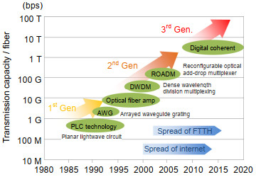
Figure 2.
Progresses in the optical communication network2.
-
Figure 3.
Demonstration of the first optical grating connected to silicon waveguides by Luxtera.
-
Figure 4.
(a–c) SEM images of a single-mode strip waveguide cross-section at different orientations. (d, e) Bending loss spectra for TE and TM polarizations, respectively. Figure reprinted with permission from ref.14, Optical Society of America.
-
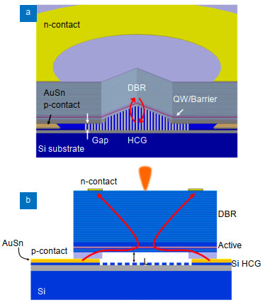
Figure 5.
Schematic of VCSEL with Si HCG as bottom mirror.
-
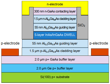
Figure 6.
Schematic layer structure of an InAs/GaAs QD laser on a Ge-on-Si substrate.
-
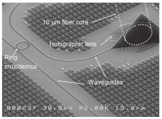
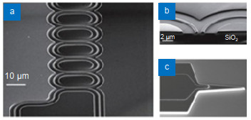
Figure 7.
SEM photographs of nano-scale Si/SiO2 waveguides.
-
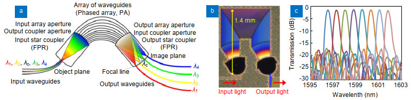
Figure 8.
(a) Schematic showing the operating principle of the AWG. (b) Photomicrograph of the AWG with about 1.4 mm square and eight wavelength channels. (c) Filter spectral characteristics. Figure reprinted with permission from: (b, c) ref.38, OKI Corporate.
-
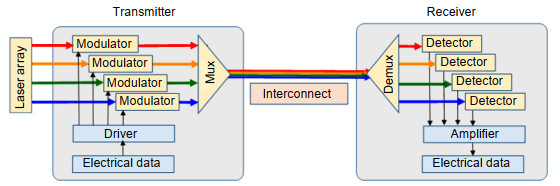
Figure 9.
Basic block diagram of an optical link including a transmitter and receiver.
-
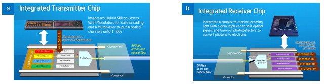
Figure 10.
50 Gb/s Si photonics transmit module.
-
Figure 11.
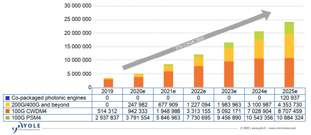
Silicon photonics shipments, for datacenter (in units) 2019-2025e.
-
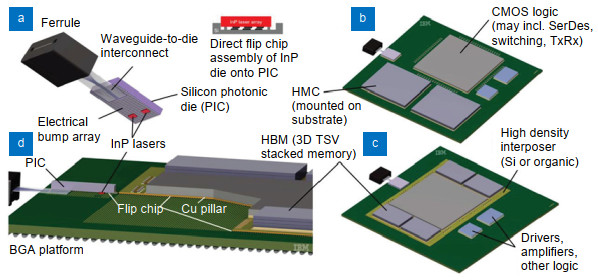
Figure 12.
Si photonic MCM.
-
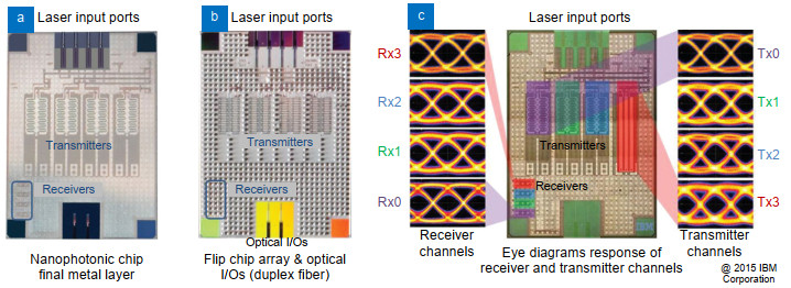
Figure 13.
IBM Si CWDM 4 × 25 Gb/s die.
-
Figure 14.
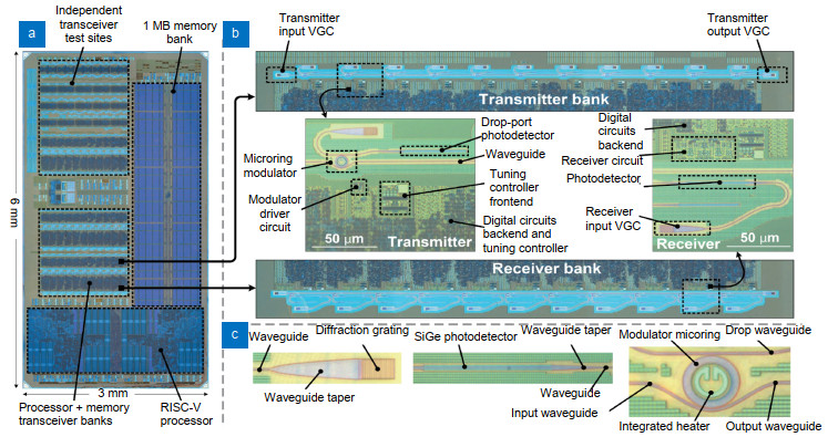
Schematic cross-section of 45 nm SOI CMOS process based Si photonic platform with photonic as well as electronic devices at the front end and bump at the back end.
-
Figure 15.
Photograph of "Zero-change" SOI platform die.
-
Figure 16.
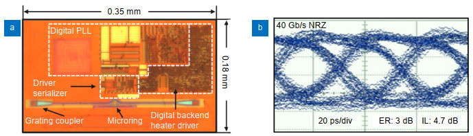
40 Gb/s transmitters.
-
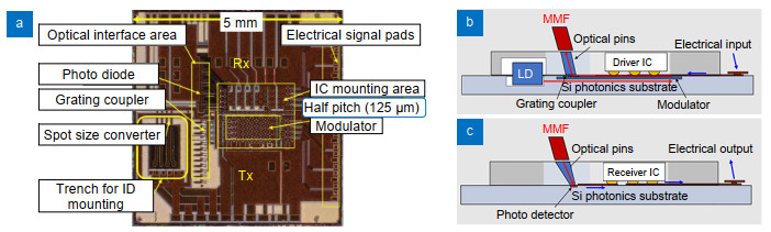
Figure 17.
(a) Whole part of optical I/O core chip. (b, c) Cross-sectional views of receiver and transmitter, respectively. Figure reprinted with permission from ref.61. AIOCORE.
-
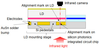
Figure 18.
Cross-sectional view of Si photonics integrated circuit with FP-LD.
-
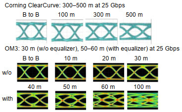
Figure 19.
Transmission characteristics of the optical I/O core with two kinds of MMFs.
-
Figure 20.
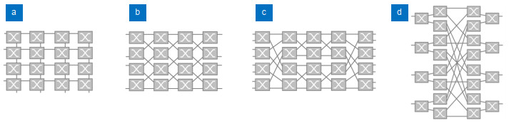
Schematic of typical optical switch topologies.
-
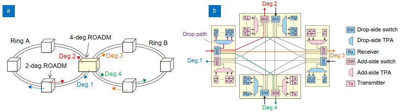
Figure 21.
(a) Example of multi-ring network. (b) 4-degree ROADM node configuration connecting two ring networks. Figure reprinted with permission from ref.69, NTT Technical Review.
-
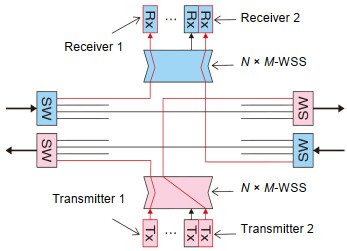
Figure 22.
Configurations of colorless, directionless and contention-less TPA's for ROADM.
-
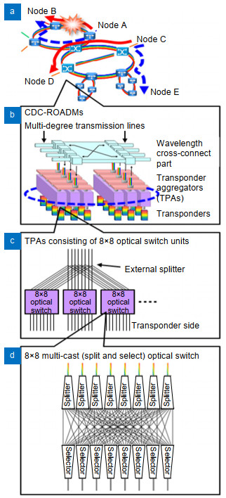
Figure 23.
(a) Two cases of reconfiguring optical paths in photonic networks with CDC-ROADMs. (b) Schematic of CDC-ROADM. (c) TPA consisting of multiple optical switch modules. (d) Configuration of 8 × 8 multi-cast optical switch. Figure reprinted with permission from ref.75, IEEE.
-
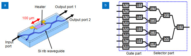
Figure 24.
Polarization-independent Si photonic MZ switch and 8×1 selector.
-
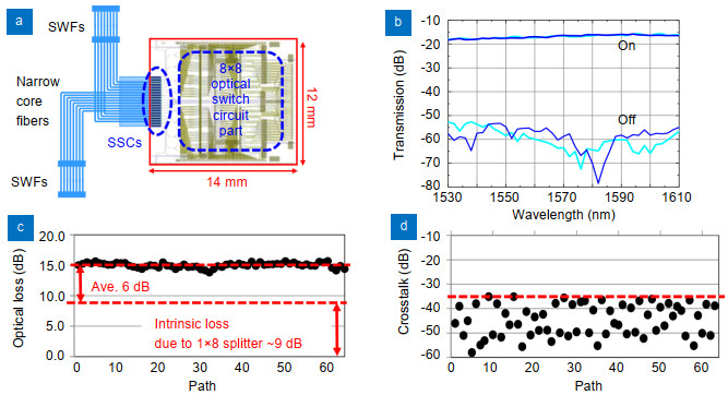
Figure 25.
(a) Schematic of optical switch module consisting of Si chip and fiber array. (b) Measured optical transmission spectra showing on and off levels. (c) Measured optical loss of all 64 paths. (d) Measured cross-talk. Figure reprinted with permission from ref.75, IEEE.
-
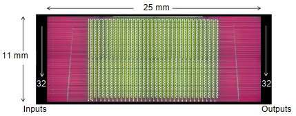
Figure 26.
32 × 32 Si TO MZI-based PILOSS switch.
-
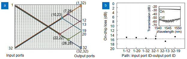
Figure 27.
Transmission characteristics of the six sampled optical paths 1-12, 1-20, 1-32, 32-1, 32-13, and 32-19.
-
Figure 28.
32 × 32 Si EO MZI-based Beneš switch.
-
Figure 29.
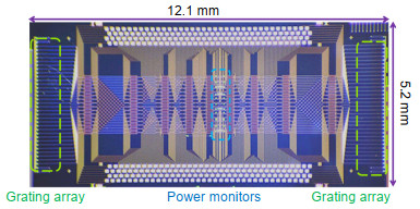
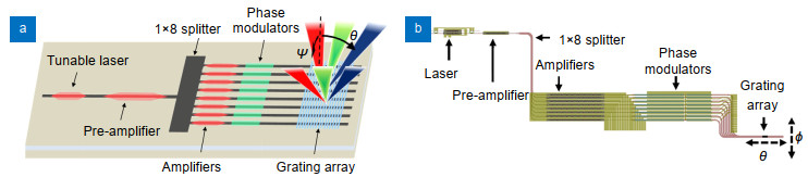
(a) Schematic configuration of hybrid Si free-space source with integrated beam steering. (b) Layout of the overall devices. Figure reprinted with permission from ref.104, SPIE.
-
Figure 30.
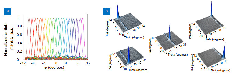
(a) Measured beam profiles at 1555 nm wavelength as the beam was swept across the field of view in the ψ axis at 1° increments. (b) Plots of the 2D beam profiles at the corners and center of the field of view. Figure reprinted with permission from ref.109, Optical Society of America.
-
Figure 31.
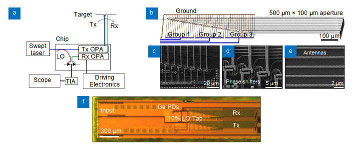
(a) Schematic of the solid-state LiDAR system with transmitting and receiving optical phased arrays. (b) 3D picture of the optical phased array. (c–e) SEM images of phase shifter, magnified one and antenna, respectively. (f) Optical micrograph of the device. Figure reprinted with permission from ref.117, Optical Society of America.


