
 E-mail Alert
 RSS
RSS
| Citation: |
Maragkakis G M, Psilodimitrakopoulos S, Mouchliadis L, Paradisanos I, Lemonis A et al. Imaging the crystal orientation of 2D transition metal dichalcogenides using polarization-resolved second-harmonic generation. Opto-Electron Adv 2, 190026 (2019). doi: 10.29026/oea.2019.190026

|
Imaging the crystal orientation of 2D transition metal dichalcogenides using polarization-resolved second-harmonic generation
-
Abstract
We use laser-scanning nonlinear imaging microscopy in atomically thin transition metal dichalcogenides (TMDs) to reveal information on the crystalline orientation distribution, within the 2D lattice. In particular, we perform polarization-resolved second-harmonic generation (PSHG) imaging in a stationary, raster-scanned chemical vapor deposition (CVD)-grown WS2 flake, in order to obtain with high precision a spatially resolved map of the orientation of its main crystallographic axis (armchair orientation). By fitting the experimental PSHG images of sub-micron resolution into a generalized nonlinear model, we are able to determine the armchair orientation for every pixel of the image of the 2D material, with further improved resolution. This pixel-wise mapping of the armchair orientation of 2D WS2 allows us to distinguish between different domains, reveal fine structure, and estimate the crystal orientation variability, which can be used as a unique crystal quality marker over large areas. The necessity and superiority of a polarization-resolved analysis over intensity-only measurements is experimentally demonstrated, while the advantages of PSHG over other techniques are analysed and discussed. -

-
References
[1] Novoselov K S, Jiang D, Schedin F, Booth T J, Khotkevich V V et al. Two-dimensional atomic crystals. Proc Natl Acad Sci USA 102, 10451-10453 (2005). doi: 10.1073/pnas.0502848102 [2] Novoselov K S, Geim A K, Morozov S V, Jiang D, Zhang Y et al. Electric field effect in atomically thin carbon films. Science 306, 666-669 (2004). doi: 10.1126/science.1102896 [3] Mak K F, Lee C, Hone J, Shan J, Heinz T F. Atomically thin MoS2: a new direct-gap semiconductor. Phys Rev Lett 105, 136805 (2010). doi: 10.1103/PhysRevLett.105.136805 [4] Splendiani A, Sun L, Zhang Y B, Li T S, Kim J et al. Emerging photoluminescence in monolayer MoS2. Nano Lett 10, 1271-1275 (2010). doi: 10.1021/nl903868w [5] Xiao D, Liu G B, Feng W X, Xu X D, Yao W. Coupled spin and valley physics in monolayers of MoS2 and other group-VI dichalcogenides. Phys Rev Lett 108, 196802 (2012). doi: 10.1103/PhysRevLett.108.196802 [6] Mak K F, He K L, Shan J, Heinz T F. Control of valley polarization in monolayer MoS2 by optical helicity. Nat Nanotechnol 7, 494-498 (2012). doi: 10.1038/nnano.2012.96 [7] Zeng H L, Dai J F, Yao W, Xiao D, Cui X D. Valley polarization in MoS2 monolayers by optical pumping. Nat Nanotechnol 7, 490-493 (2012). doi: 10.1038/nnano.2012.95 [8] Kioseoglou G, Hanbicki A T, Currie M, Friedman A L, Gunlycke D et al. Valley polarization and intervalley scattering in monolayer MoS2. Appl Phys Lett 101, 221907 (2012). doi: 10.1063/1.4768299 [9] Radisavljevic B, Radenovic A, Brivio J, Giacometti V, Kis A. Single-layer MoS2 transistors. Nat Nanotechnol 6, 147-150 (2011). doi: 10.1038/nnano.2010.279 [10] Wang G, Chernikov A, Glazov M M, Heinz T F, Marie X et al. Colloquium: excitons in atomically thin transition metal dichalcogenides. Rev Mod Phys 90, 021001 (2018). doi: 10.1103/RevModPhys.90.021001 [11] Paradisanos I, Germanis S, Pelekanos N T, Fotakis C, Kymakis E et al. Room temperature observation of biexcitons in exfoliated WS2 monolayers. Appl Phys Lett 110, 193102 (2017). doi: 10.1063/1.4983285 [12] Ferrari A C, Bonaccorso F, Fal'ko V, Novoselov K S, Roche S et al. Science and technology roadmap for graphene, related two-dimensional crystals, and hybrid systems. Nanoscale 7, 4598-4810 (2015). doi: 10.1039/C4NR01600A [13] Wang Q H, Kalantar-Zadeh K, Kis A, Coleman J N, Strano M S. Electronics and optoelectronics of two-dimensional transition metal dichalcogenides. Nat Nanotechnol 7, 699-712 (2012). doi: 10.1038/nnano.2012.193 [14] Mak K F, Shan J. Photonics and optoelectronics of 2D semiconductor transition metal dichalcogenides. Nat Photonics 10, 216-226 (2016). doi: 10.1038/nphoton.2015.282 [15] Bonaccorso F, Colombo L, Yu G H, Stoller M, Tozzini V et al. Graphene, related two-dimensional crystals, and hybrid systems for energy conversion and storage. Science 347, 1246501 (2015). doi: 10.1126/science.1246501 [16] Schaibley J R, Yu H Y, Clark G, Rivera P, Ross J S et al. Valleytronics in 2D materials. Nat Rev Mater 1, 16055 (2016). doi: 10.1038/natrevmats.2016.55 [17] Kalantar-zadeh K, Ou J Z, Daeneke T, Strano M S, Pumera M et al. Two-dimensional transition metal dichalcogenides in biosystems. Adv Funct Mater 25, 5086-5099 (2015). doi: 10.1002/adfm.201500891 [18] Li X, Shan J Y, Zhang W Z, Su S, Yuwen L H et al. Recent advances in synthesis and biomedical applications of two-dimensional transition metal dichalcogenide nanosheets. Small 13, 1602660 (2017). doi: 10.1002/smll.201602660 [19] Najmaei S, Yuan J T, Zhang J, Ajayan P, Lou J. Synthesis and defect investigation of two-dimensional molybdenum disulfide atomic layers. Acc Chem Res 48, 31-40 (2015). doi: 10.1021/ar500291j [20] Zou X L, Yakobson B I. An open canvas-2D materials with defects, disorder, and functionality. Acc Chem Res 48, 73-80 (2015). doi: 10.1021/ar500302q [21] Paradisanos I, Pliatsikas N, Patsalas P, Fotakis C, Kymakis E et al. Spatial non-uniformity in exfoliated WS2 single layers. Nanoscale 8, 16197-16203 (2016). doi: 10.1039/C6NR03597C [22] van der Zande A M, Huang P Y, Chenet D A, Berkelbach T C, You Y M et al. Grains and grain boundaries in highly crystalline monolayer molybdenum disulphide. Nat Mater 12, 554-561 (2013). doi: 10.1038/nmat3633 [23] Psilodimitrakopoulos S, Mouchliadis L, Paradisanos I, Lemonis A, Kioseoglou G et al. Ultrahigh-resolution nonlinear optical imaging of the armchair orientation in 2D transition metal dichalcogenides. Light Sci Appl 7, 18005 (2018). doi: 10.1038/lsa.2018.5 [24] Kumar N, Najmaei S, Cui Q N, Ceballos F, Ajayan P M et al. Second harmonic microscopy of monolayer MoS2. Phys Rev B 87, 161403 (2013). doi: 10.1103/PhysRevB.87.161403 [25] Malard L M, Alencar T V, Barboza A P M, Mak K F, de Paula A M. Observation of intense second harmonic generation from MoS2 atomic crystals. Phys Rev B 87, 201401 (2013). doi: 10.1103/PhysRevB.87.201401 [26] Li Y L, Rao Y, Mak K F, You Y M, Wang S Y et al. Probing symmetry properties of few-layer MoS2 and h-BN by optical second-harmonic generation. Nano Lett 13, 3329-3333 (2013). doi: 10.1021/nl401561r [27] Yin X B, Ye Z L, Chenet D A, Ye Y, O'Brien K et al. Edge nonlinear optics on a MoS2 atomic monolayer. Science 344, 488-490 (2014). doi: 10.1126/science.1250564 [28] Clark D J, Senthilkumar V, Le C T, Weerawarne D L, Shim B et al. Strong optical nonlinearity of CVD-grown MoS2 monolayer as probed by wavelength-dependent second-harmonic generation. Phys Rev B 90, 121409 (2014). doi: 10.1103/PhysRevB.90.121409 [29] Hsu W T, Zhao Z A, Li L J, Chen C H, Chiu M H et al. Second harmonic generation from artificially stacked transition metal dichalcogenide twisted bilayers. ACS Nano 8, 2951-2958 (2014). doi: 10.1021/nn500228r [30] Wang Y, Xiao J, Yang S, Wang Y, Zhang X. Second harmonic generation spectroscopy on two-dimensional materials[Invited]. Opt Mater Express 9, 1136-1149 (2019). doi: 10.1364/OME.9.001136 [31] Zhao M, Ye Z L, Suzuki R, Ye Y, Zhu H Y et al. Atomically phase-matched second-harmonic generation in a 2D crystal. Light Sci Appl 5, e16131 (2016). doi: 10.1038/lsa.2016.131 [32] Boyd R W. Nonlinear Optics 3rd ed (Academic Press, San Diego, 2008). -
Supplementary Information
Supplementary information for Imaging the crystal orientation of 2D transition metal dichalcogenides using polarization-resolved second-harmonic generation 
oea-2019-0026 PSHG modulation.avi
-
Access History
Figures(7)
Tables(1)
Article Metrics


Export File
Citation
Maragkakis G M, Psilodimitrakopoulos S, Mouchliadis L, Paradisanos I, Lemonis A et al. Imaging the crystal orientation of 2D transition metal dichalcogenides using polarization-resolved second-harmonic generation. Opto-Electron Adv 2, 190026 (2019). doi: 10.29026/oea.2019.190026
Format
Content
 DownLoad:

-
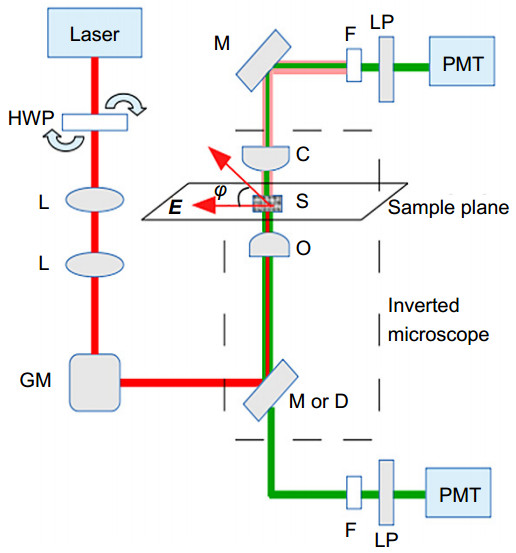
Figure 1.
Schematic representation of the experimental setup, also adopted in ref.23, allowing high-resolution PSHG measurements in stationary, raster-scanned samples.
-
Figure 3.
The experimental configuration, showing the laboratory X-Y-Z, and the crystalline x-y-z coordinate systems.
-
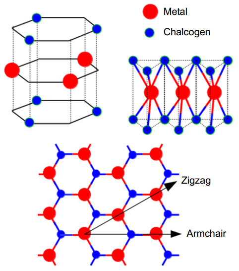
Figure 2.
Schematic representation of the structure of 2D TMDs, containing three sublattices, with a plane of metal atoms being hexagonally packed between two planes of chalgogen atoms.
-
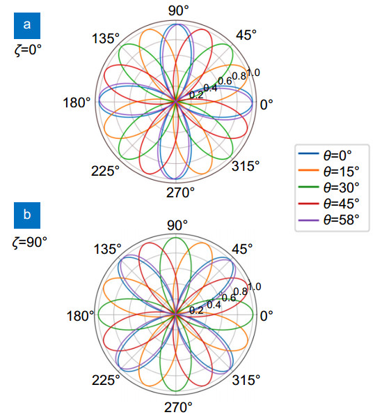
Figure 4.
Simulated PSHG modulation presented in polar diagrams, as function of the linear polarization orientation φ, with φ ϵ [1°, 360°], for fixed polarizer at angle (a) ζ=0° and (b) ζ=90°.
-
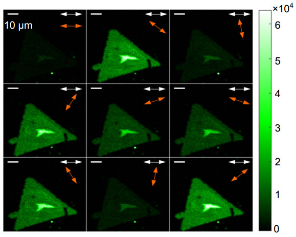
Figure 5.
Snapshots of experimental PSHG images of a WS2 flake, CVD-grown on a sapphire substrate.
-
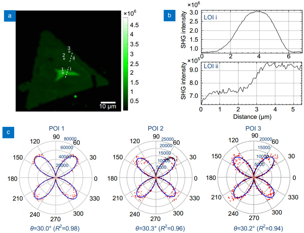
Figure 6.
(a) Integration of the experimentally detected PSHG intensity from the WS2 island, for φ ϵ[0°–90°] with step 1°, presented upon marking three POIs and two LOIs for further analysis. The POIs are actually single pixels of the 1200×1200 original image, magnified here, for illustration purposes. (b) Intensity profile of the experimental PSHG modulation presented in (a), along the LOIs shown there. As may be seen for LOI i, the intensity in the central, brighter area is magnified by a factor of ~4, which suggests the presence of second layer29. (c) Polar diagrams of the experimental PSHG modulation for φ ϵ[0°–360°] with step 1°, for the POIs illustrated in (a). We show with red color the raw data, and with blue the fitting using Eq. (3). We also present the retrieved values of the armchair orientation θ and the quality of fitting R2.
-
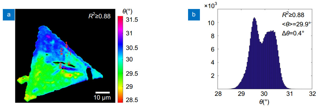
Figure 7.
Mapping in (a) 2D diagram and (b) histogram of the armchair orientation distribution of the WS2 flake (with < θ > being the mean vale), based on the pixel-by- pixel fitting (R2≥0.88) of Eq. (3) on the experimental PSHG modulation for φ ϵ[0°–360°] with step 1°.


