
 E-mail Alert
 RSS
RSS
Theoretical investigation of surface plasmonic polariton-based electro-optical modulator with low polarization dependence
-
摘要:
由于受到表面等离激元(SPP)固有偏振性的影响,基于表面等离激元的波导型调制器只支持横磁模式(TM)传播。本文提出了一种在垂直方向和水平方向上均构建混合(hybrid)波导结构的表面等离激元电光调制器,以实现调制器的低偏振灵敏性。在组合的混合波导中,垂直和水平偏振方向上的表面等离激元被限制在相应的混合波导中。通过调控介质和ITO界面处形成载流子积累层中载流子浓度可实现光吸收调制。在经优化的结构中两个偏振态的消光比差为0.005 dB/μm。通过3D-FDTD模拟调制器的光场调控,清楚地显示了传统硅波导与偏振不灵敏调制器间的耦合传输特性。两种偏振态下,偏振不灵敏调制器与硅波导之间的耦合效率均达到了74%以上。此项研究将为表面等离激元电光调制器在偏振不灵敏光集成回路中的应用提供解决方案,为其与具有偏振随机态光纤回路的集成奠定了基础。
 Abstract:
Plasmonic modulators essentially support only transverse magnetic mode. A plasmonic modulator consisting of hybrid plasmonic waveguides in both vertical and horizontal directions is proposed to reduce the polarization-dependence. In a combined waveguide, surface plasmon polariton (SPP) modes polarized in the vertical and horizontal directions exist in the correspondingly oriented hybrid plasmonic waveguide. The light modulation is investigated by tuning the carrier density of the accumulated layer where occurs at the dielectric-ITO interfaces. In an optimized structure, a ΔIER (a difference between the extinction ratios of two polarization modes) under 0.01 dB/μm is demonstrated at ITO "ENZ"-state by simulation. The energy flux clearly shows the polarization-selective coupling between the polarized guided modes in the feeding silicon waveguide and those in the combined waveguide. Coupling efficiency above 74% is obtained for both polarizations. The proposed plasmonic combined modulator has a potential application in guiding and processing of light from a fiber with a random polarization state.
-
Key words:
- surface plasmon polaritons /
- transparent conductive oxide /
- modulator /
- polarization
-

Overview: Photonic integratedcircuits (PICs) have made remarkable progress in the past few decades with thedevelopment of applications in the fields of optical communication, sensing,and imaging. Si photonics is deemed to be a promising solution for futurehigh-speed on/off-chip optical interconnections. Typical Si waveguide modulatorsleverage electrically altering either the refractive or the absorptiveproperties of a material to modulate the transmission of light through adevice. Due to the weak plasma dispersion effect of Si and the diffractionlimit of the Si waveguides, the Si MZI modulators suffer from large footprintsof ~103 μm2~104 μm2. Plasmonics provides an approach tominiaturize optical devices beyond the diffraction limit. Alternatively, fullyCMOS-compatible plasmonic modulators using Si as an active material aredemonstrated. Relying on the manipulation of the transverse magnetic (TM) modeexcited on the metal-dielectric interface, most of the previous demonstrationsare designed to response only for specific polarization state. In this case, itwill lead to a high polarization dependent loss, when the polarizationsensitive modulator integrates to a fiber with random polarization state.Herein, we propose a plasmonic modulator utilizing a metal-oxide- indium tin oxide(ITO) wrap-around the silicon waveguide and investigate its optical modulationability for both the vertical and horizontal polarized guiding light by tuningelectro-absorption of ITO with the field-induced carrier injection. ITO wasreported to have much larger variation of its dielectric constant. Similar toSi based field-effect, MOS device where carrier accumulation is formed under anapplied voltage bias, carrier density (NITO) can be tuned at the ITO/dielectricinterface with an applied bias. When the real part of the permittivity of theITO material is tuned to near zero, at a certain NITO, which is referred as the“epsilon-near-zero” (ENZ) state, while it has the maximal absorption loss dueto the strong confinement of the guided mode. By simultaneously optimizing themode field confinement and the ITO carrier dispersion effect in these stacks,similar optical modulation performance can be achieved for both polarizations,which has not been reported in the previous work. In an optimized structure, aΔER (a difference between the extinction ratios of two polarizationmodes) about 0.005 dB/μm is demonstrated at ITO “ENZ”-state by simulation. Theenergy flux clearly shows the polarization-selective coupling between the polarizedguided modes in the feeding silicon waveguide and those in the combinedwaveguide. Coupling efficiency above 74% is obtained for both polarizations.The proposed plasmonic combined modulator has a potential application inguiding and processing of light from a fiber with a random polarization state.
-

-
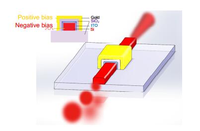
图 1 基于表面等离激元电吸收调制器3D图。插图为调制器的截面图
Figure 1. 3D view of the proposed EA plasmonic modulator. Inset is the cross-section of the modulator
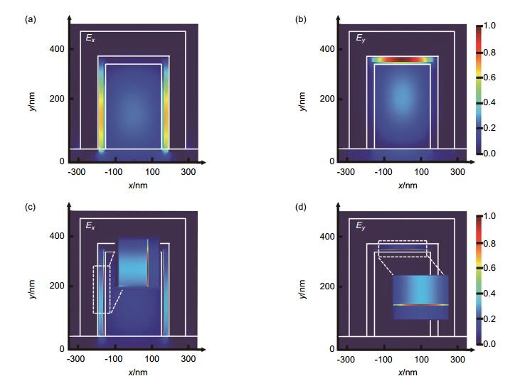
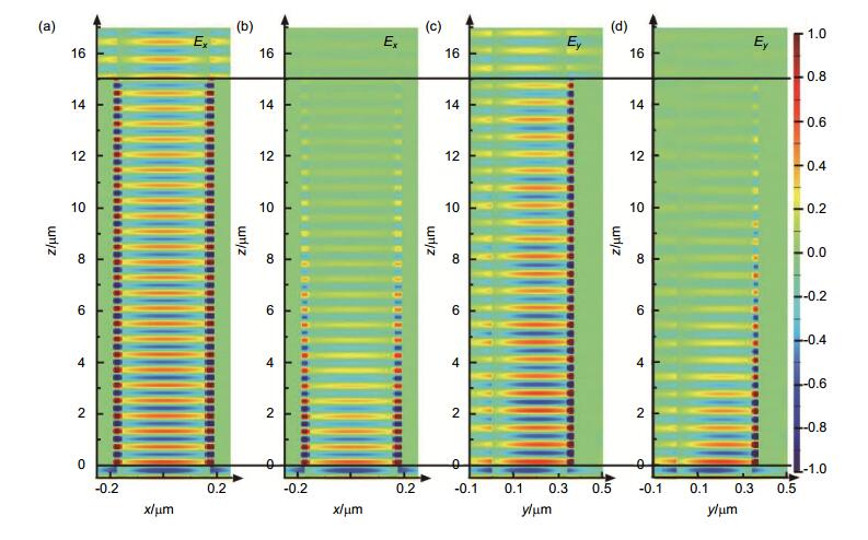
图 2 (a),(b)分别为器件未加电时TE模和TM的电场分布;(c),(d)分别为器件加电后TE模和TM的电场分布
Figure 2. Electric field profiles Ex and Ey of the modulator for (a), (b) "ON" state, and (c), (d) "OFF" state, respectively
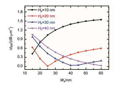
图 3 SiO2层厚度对两个偏振下的消光比差的影响
Figure 3. ∆IER of the EA modulator versus Wp at Hp=10 nm~40 nm
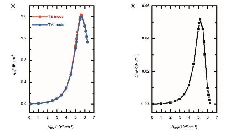
图 4 载流子积累层中载流子浓度变化对电光调制器IER (a)和ΔIER (b)的影响
Figure 4. IER (a) and ∆IER (b) as a function of average carrier concentration of ITO layer NITO for the EA modulator
-
[1] Pu M B, Yao N, Hu C G, et al. Directional coupler and nonlinear Mach-Zehnder interferometer based on metal-insulator-metal plasmonic waveguide[J]. Optics Express, 2010, 18(20): 21030-21037. doi: 10.1364/OE.18.021030
[2] Akiyama S, Baba T, Imai M, et al. 50-Gb/s silicon modulator using 250-mm-Long phase shifter based-on forward-biased pin diodes[C]//Proceedings of the 9th International Conference on Group IV Photonics, San Diego, 2012.
[3] 蒲明博, 王长涛, 王彦钦, 等.衍射极限尺度下的亚波长电磁学[J].物理学报, 2017, 66(14):144101. doi: 10.7498/aps.66.144101
Pu M B, Wang C T, Wang Y Q, et al. Subwavelength electromagnetics below the diffraction limit[J]. Acta Physica Sinica, 2017, 66(14):144101. doi: 10.7498/aps.66.144101
[4] Dionne J A, Diest K, Sweatlock L A, et al. PlasMOStor: a Metal-Oxide-Si field effect plasmonic modulator[J]. Nano Letters, 2009, 9(2): 897-902. doi: 10.1021/nl803868k
[5] Feigenbaum E, Diest K, Atwater H A. Unity-order index change in transparent conducting oxides at visible frequencies[J]. Nano Letters, 2010, 10(6): 2111-2116. doi: 10.1021/nl1006307
[6] Traviss D, Bruck R, Mills B, et al. Ultrafast plasmonics using transparent conductive oxide hybrids in the epsilon-near-zero regime[J]. Applied Physics Letters, 2013, 102(12): 121112. doi: 10.1063/1.4798833
[7] Noginov M A, Gu L, Livenere J, et al. Transparent conductive oxides: plasmonic materials for telecom wavelengths[J]. Applied Physics Letters, 2011, 99(2): 021101. doi: 10.1063/1.3604792
[8] Lu Z L, Zhao W S, Shi K F. Ultracompact electroabsorption modulators based on tunable Epsilon-Near-Zero-Slot waveguides[J]. IEEE Photonics Journal, 2012, 4(3):735-740. doi: 10.1109/JPHOT.2012.2197742
[9] Sorger V J, Lanzillotti-Kimura N D, Ma R M, et al. Ultra-compact silicon nanophotonic modulator with broadband response[J]. Nanophotonics, 2012, 1(1): 17-22. doi: 10.1515/nanoph-2012-0009
[10] Lee H W, Papadakis G, Burgos S P, et al. Nanoscale conducting oxide PlasMOStor[J]. Nano Letters, 2014, 14(11): 6463-6468. doi: 10.1021/nl502998z
[11] Zhu S Y, Lo G Q, Kwong D L. Design of an ultra-compact electro-absorption modulator comprised of a deposited TiN/HfO2/ITO/Cu stack for CMOS backend integration[J]. Optics Express, 2014, 22(15): 17930-17947. doi: 10.1364/OE.22.017930
[12] Krasavin A V, Zayats A V. Photonic signal processing on electronic scales: electro-optical field-effect nanoplasmonic modulator[J]. Physical Review Letters, 2012, 109(5): 053901. doi: 10.1103/PhysRevLett.109.053901
[13] Vasudev A P, Kang J H, Park J, et al. Electro-optical modulation of a silicon waveguide with an " epsilon-near-zero" material[J]. Optics Express, 2013, 21(22): 26387-26397. doi: 10.1364/OE.21.026387
[14] Johnson P B, Christy R W. Optical constants of the noble metals[J]. Physical Review B, 1972, 6(12): 4370. doi: 10.1103/PhysRevB.6.4370
[15] Jin L, Chen Q, Song S C. Plasmonic waveguides with low polarization dependence[J]. Optics Letters, 2013, 38(16): 3078-3081. doi: 10.1364/OL.38.003078
-
 下载:
下载:
 点击扫一扫
点击扫一扫
图(5)
计量
- 文章访问数: 6530
- PDF下载数: 2755
- 施引文献: 0


